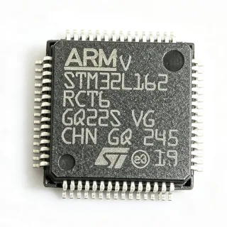
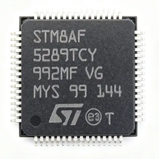
STM32G484RET6 - 170MHz Arm Cortex-M4 MCU with FPU | STMicroelectronics
Référence : STM32G484RET6 ✓ Actif| Qté | Prix unitaire | Total |
|---|---|---|
| 1 | $8.5 | $8,50 |
| 10 | $7.65 | $76,50 |
| 100 | $6.8 | $680,00 |
| 500 | $6.12 | $3 060,00 |
| 1 000 | $5.44 | $5 440,00 |
STM32G484RET6 Présentation
What is a microcontroller? A microcontroller (MCU) is a compact integrated circuit designed to govern a specific operation in an embedded system. It integrates a processor core, memory, and programmable input/output peripherals on a single chip. In the system hierarchy, an MCU sits above a microprocessor (which lacks integrated memory and peripherals) and below a system-on-chip (SoC) that may include more complex subsystems. The STM32G484RET6 is a mid-range MCU in the STM32 family, balancing performance, power efficiency, and peripheral integration.
Key features include a 170 MHz Arm Cortex-M4 core with FPU and DSP instructions, 512 KB flash, 128 KB SRAM, and a comprehensive set of peripherals: three 12-bit ADCs (up to 5 Msps), four comparators, three operational amplifiers, a 12-bit DAC, and advanced timers with dead-time generation for motor control. It also includes a CORDIC hardware accelerator and a FMAC (filter math accelerator) for mathematical processing. The device supports multiple communication interfaces: I2C, SPI, UART, CAN FD, and USB.
The STM32G484RET6 is built on ST's advanced 90 nm process technology, offering a balance of performance and power consumption. The core is based on the Armv7E-M architecture, which includes hardware divide and single-cycle multiply-accumulate instructions. The FPU enables efficient floating-point arithmetic, essential for control algorithms. The device also features a memory protection unit (MPU) and a nested vectored interrupt controller (NVIC) for real-time responsiveness.
Typical applications include field-oriented control (FOC) of brushless DC motors, digital power supplies (buck, boost, and flyback converters), solar inverters, and industrial automation. The high-resolution timers (HRTIM) with 184 ps resolution are ideal for power conversion topologies. The device also supports USB Power Delivery (PD) for charging applications.
When designing with this MCU, ensure proper decoupling of the power supply pins with 100 nF capacitors placed close to each VDD pin. The VDDA analog supply should be filtered with a ferrite bead and a 1 uF capacitor to reduce noise. For motor control applications, use the dedicated timer break inputs for safe shutdown.
Alternatives de remplacement direct pour STM32G484RET6 — même boîtier, compatible broche à broche. Les références à boîtier différent nécessitant une retouche du PCB sont exclues.
Variantes de cette série
Modèles de la même série directement compatibles avec STM32G484RET6 (même facteur de forme et même empreinte) — différant par Core, Package, Flash Memory, SRAM, Communication Interfaces.
Outil de comparaison rapide — sélectionnez des références alternatives pour une comparaison côte à côte :
STM32G474RET6
✅ Remplacement direct✓ En stock
$8.25 / unité
Voir la fiche technique →STM32G484RET6TR
✅ Remplacement direct📋 Alternative de référence (hors catalogue)
STM32G484RET6 Valeurs maximales et caractéristiques électriques
| Core | Arm Cortex-M4 with FPU |
| Max Clock Frequency | 170 MHz |
| Flash Memory | 512 KB |
| SRAM | 128 KB |
| Boîtier | LQFP-64 |
| Operating Voltage | 1.71 V to 3.6 V |
| Température de fonctionnement | -40C to +85C |
| ADC Resolution | 12-bit |
| ADC Sample Rate | 5 Msps |
| DAC Resolution | 12-bit |
| Number of Timers | 10 (including HRTIM) |
| Communication Interfaces | I2C, SPI, UART, CAN FD, USB |
| GPIO Pins | 51 |
| DMA Channels | 16 |
| Statut RoHS | Compliant |
Configuration des broches de STM32G484RET6
| Broche 1 | VBAT — Battery backup supply |
| Broche 2 | PC13 — GPIO / RTC output |
| Broche 3 | PC14 — GPIO / OSC32_IN |
| Broche 4 | PC15 — GPIO / OSC32_OUT |
| Broche 5 | PF0 — GPIO |
| Broche 6 | PF1 — GPIO |
| Broche 7 | NRST — Reset (active low) |
| Broche 8 | VDD — Digital power supply |
| Broche 9 | VSS — Digital ground |
| Broche 10 | VDDA — Analog power supply |
| Broche 11 | PA0 — GPIO / ADC input |
| Broche 12 | PA1 — GPIO / ADC input |
| Broche 13 | PA2 — GPIO / USART2_TX |
| Broche 14 | PA3 — GPIO / USART2_RX |
| Broche 15 | PA4 — GPIO / DAC_OUT1 |
| Broche 16 | PA5 — GPIO / DAC_OUT2 |
| Broche 17 | PA6 — GPIO / TIM1_CH1 |
| Broche 18 | PA7 — GPIO / TIM1_CH2 |
| Broche 19 | PA8 — GPIO / TIM1_CH1N |
| Broche 20 | PA9 — GPIO / USART1_TX |
| Broche 21 | PA10 — GPIO / USART1_RX |
| Broche 22 | PA11 — GPIO / USB_DM |
| Broche 23 | PA12 — GPIO / USB_DP |
| Broche 24 | PA13 — GPIO / SWDIO |
| Broche 25 | PA14 — GPIO / SWCLK |
| Broche 26 | PA15 — GPIO / JTDI |
| Broche 27 | PB0 — GPIO / ADC input |
| Broche 28 | PB1 — GPIO / ADC input |
| Broche 29 | PB2 — GPIO / BOOT1 |
| Broche 30 | PB3 — GPIO / JTDO |
| Broche 31 | PB4 — GPIO / NJTRST |
| Broche 32 | PB5 — GPIO / I2C1_SMBA |
| Broche 33 | PB6 — GPIO / I2C1_SCL |
| Broche 34 | PB7 — GPIO / I2C1_SDA |
| Broche 35 | PB8 — GPIO / CAN1_RX |
| Broche 36 | PB9 — GPIO / CAN1_TX |
| Broche 37 | PB10 — GPIO / I2C2_SCL |
| Broche 38 | PB11 — GPIO / I2C2_SDA |
| Broche 39 | PB12 — GPIO / SPI2_NSS |
| Broche 40 | PB13 — GPIO / SPI2_SCK |
| Broche 41 | PB14 — GPIO / SPI2_MISO |
| Broche 42 | PB15 — GPIO / SPI2_MOSI |
| Broche 43 | PC0 — GPIO / ADC input |
| Broche 44 | PC1 — GPIO / ADC input |
| Broche 45 | PC2 — GPIO / ADC input |
| Broche 46 | PC3 — GPIO / ADC input |
| Broche 47 | PC4 — GPIO / ADC input |
| Broche 48 | PC5 — GPIO / ADC input |
| Broche 49 | PC6 — GPIO / TIM3_CH1 |
| Broche 50 | PC7 — GPIO / TIM3_CH2 |
| Broche 51 | PC8 — GPIO / TIM3_CH3 |
| Broche 52 | PC9 — GPIO / TIM3_CH4 |
| Broche 53 | PC10 — GPIO / USART4_TX |
| Broche 54 | PC11 — GPIO / USART4_RX |
| Broche 55 | PC12 — GPIO / USART5_TX |
| Broche 56 | PD0 — GPIO / CAN2_RX |
| Broche 57 | PD1 — GPIO / CAN2_TX |
| Broche 58 | PD2 — GPIO / TIM1_ETR |
| Broche 59 | VDD — Digital power supply |
| Broche 60 | VSS — Digital ground |
| Broche 61 | PD3 — GPIO / USART2_CTS |
| Broche 62 | PD4 — GPIO / USART2_RTS |
| Broche 63 | PD5 — GPIO / USART2_CK |
| Broche 64 | PD6 — GPIO / USART2_DE |
Applications typiques
STM32G484RET6 convient pour 6 applications: Motor Control, Digital Power Conversion, Solar Inverters, Industrial Automation, USB Power Delivery, Battery Management Systems.
Motor Control
The STM32G484RET6 is ideal for field-oriented control (FOC) of brushless DC motors. Its high-resolution timer (HRTIM) with 184 ps resolution enables precise PWM generation, while the three operational amplifiers and four comparators support current sensing and overcurrent protection. The 170 MHz Cortex-M4 core with FPU handles complex control algorithms efficiently. In a typical motor control application, the MCU reads phase currents via the ADCs, computes the FOC algorithm, and generates PWM signals to drive the inverter. The HRTIM's dead-time insertion prevents shoot-through, and the break inputs provide safe shutdown. Compared to lower-performance MCUs, the STM32G484RET6 offers faster loop times and higher resolution, improving motor efficiency and reducing torque ripple.
Recommandé
Digital Power Conversion
The STM32G484RET6 excels in digital power supplies, including buck, boost, and flyback converters. Its HRTIM provides high-resolution PWM with 184 ps resolution, essential for precise voltage regulation. The fast ADCs (5 Msps) enable high-bandwidth current and voltage sensing, while the comparators can trigger fault protection within nanoseconds. In a typical digital power supply, the MCU samples the output voltage and inductor current, runs a digital control loop (e.g., PID), and adjusts the PWM duty cycle. The CORDIC and FMAC accelerators offload mathematical computations, freeing the CPU for other tasks. Compared to analog controllers, the STM32G484RET6 offers flexibility, programmability, and higher efficiency through advanced control techniques like phase-shifted full-bridge or LLC resonant conversion.
Recommandé
Solar Inverters
The STM32G484RET6 is well-suited for solar inverters, where it manages maximum power point tracking (MPPT) and grid synchronization. Its high-resolution timers and fast ADCs enable precise control of the DC-DC boost converter and the DC-AC inverter stage. The device's multiple communication interfaces (CAN FD, UART, SPI) allow integration with monitoring systems and grid communication. In a typical solar inverter, the MCU measures panel voltage and current, runs the MPPT algorithm, and controls the boost converter to extract maximum power. It also generates sinusoidal PWM for the inverter stage, ensuring low harmonic distortion. The STM32G484RET6's robust analog front-end and high-speed processing make it a cost-effective solution for residential and commercial solar systems.
Recommandé
Industrial Automation
The STM32G484RET6 is a versatile MCU for industrial automation, including PLCs, robotic controllers, and process control. Its rich set of timers, ADCs, and communication interfaces (CAN FD, Ethernet via external PHY) enable real-time control and networking. The device's 170 MHz core and FPU handle complex algorithms like kinematics and trajectory planning. In a typical PLC, the MCU scans inputs, executes user logic, and updates outputs within a deterministic cycle time. The STM32G484RET6's fast interrupt handling and DMA support ensure low latency. Compared to older MCUs, it offers higher performance and integration, reducing system cost and board space.
Recommandé
USB Power Delivery
The STM32G484RET6 supports USB Power Delivery (PD) through its USB controller and dedicated UCPD (USB Type-C and Power Delivery) peripheral. It can negotiate power contracts and control the power path in chargers and adapters. The device's high-resolution timer and fast ADC enable precise current and voltage control for PD profiles. In a typical USB PD charger, the MCU communicates with the sink device to negotiate voltage and current levels, then controls a buck converter to deliver the required power. The STM32G484RET6's integrated analog peripherals reduce external component count, making it a compact solution for fast chargers.
Recommandé
Battery Management Systems
The STM32G484RET6 is used in battery management systems (BMS) for electric vehicles and energy storage. Its multiple ADCs and comparators enable accurate cell voltage and current monitoring, while the CAN FD interface supports communication with the vehicle's main controller. The device's high-speed processing allows real-time state-of-charge (SoC) and state-of-health (SoH) estimation. In a typical BMS, the MCU measures each cell's voltage, balances cells, and protects against overcurrent and overvoltage. The STM32G484RET6's robust design and wide operating temperature range make it suitable for automotive environments.
Recommandé
Récapitulatif des produits recommandés
Données de référence d'ingénierie pour STM32G484RET6 — comparaison, recommandations de conception et informations de conformité.
Guide de sélection
Comparaison avec les alternatives
| Paramètre | Ce produit | STM32G474RET6 | STM32G484RET6TR | STM32G484VET6 | LPC54608J512BD208 |
|---|---|---|---|---|---|
| Package | LQFP-64 | LQFP-64 (same) | LQFP-64 (same) | LQFP-100 (different) | LQFP-208 (different) |
| Brand | STMicroelectronics | STMicroelectronics | STMicroelectronics | STMicroelectronics | NXP Semiconductors |
| Core | Arm Cortex-M4 with FPU | Arm Cortex-M4 with FPU | Arm Cortex-M4 with FPU | Arm Cortex-M4 with FPU | Arm Cortex-M4 with FPU |
| Max Clock Frequency | 170 MHz | 170 MHz | 170 MHz | 170 MHz | 180 MHz |
| Flash Memory | 512 KB | 512 KB | 512 KB | 512 KB | 512 KB |
| SRAM | 128 KB | 128 KB | 128 KB | 128 KB | 200 KB |
| CORDIC Accelerator | Yes | No | Yes | Yes | No |
| FMAC Accelerator | Yes | No | Yes | Yes | No |
Principaux différenciateurs
- CORDIC and FMAC hardware accelerators (vs STM32G474RET6)
- High-resolution timer (HRTIM) with 184 ps resolution (vs LPC54608J512BD208)
- Integrated analog peripherals (3 op-amps, 4 comparators) (vs LPC54608J512BD208)
Notes de conception
Decouple each VDD pin with a 100 nF ceramic capacitor placed as close as possible to the pin. Additionally, place a 4.7 uF capacitor on the VDDA pin and a 1 uF capacitor on the VREF+ pin. Use a ferrite bead between VDD and VDDA to filter high-frequency noise. Ensure the power supply can handle the peak current of the MCU, especially during flash programming or high-speed GPIO toggling.
For the LQFP-64 package, use a 4-layer PCB with a solid ground plane. Route the crystal oscillator (HSE) with short traces and keep them away from high-speed digital signals. Place the decoupling capacitors on the same side as the MCU, close to the pins. For motor control applications, separate the power ground from the analog ground and connect them at a single point.
Ensure the BOOT0 pin is properly configured to select the correct boot mode. For debugging, connect SWDIO and SWCLK with pull-up resistors. Do not exceed the absolute maximum ratings for VDD (3.6 V) and VDDA (3.6 V). When using the HRTIM, verify that the dead-time settings are correct to prevent shoot-through in the power stage.
Informations de conformité
RoHS and REACH compliant per STMicroelectronics product page. Not AEC-Q100 qualified; for automotive, consider STM32G4A1 series.