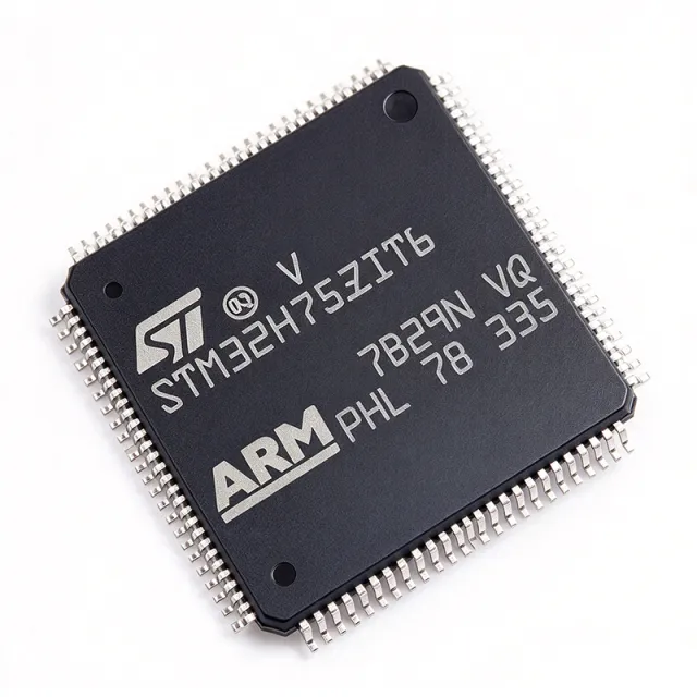
Quick Answers — What is the STM32H753ZIT6?
The STM32H753ZIT6 is an active, high-performance 32-bit Arm Cortex-M7 microcontroller from STMicroelectronics, available in the XAIPART database with 18,000 units in stock. It runs at up to 480 MHz and integrates 2 MB of dual-bank Flash, 1 MB of SRAM, a double-precision FPU, a 16-bit 3.6 MSPS ADC, a 12-bit DAC, 10/100 Ethernet MAC with DMA, USB OTG HS/FS, CAN FD, a Chrom-ART 2D accelerator, and a hardware cryptographic processor. The device comes in a 144-pin LQFP package measuring 20 x 20 mm with a 0.5 mm lead pitch, operates from 1.62 V to 3.6 V, and is rated for -40 C to +85 C.
Engineers choose the STM32H753ZIT6 when an embedded design needs substantial real-time processing, field-updatable firmware, mixed analog and digital peripherals, and multiple communication interfaces without adding separate protocol or graphics controllers. Its 2 MB dual-bank Flash supports read-while-write operation, while 1 MB of SRAM provides space for control loops, network buffers, audio data, or intermediate processing results. Review the STM32H753ZIT6 product page for sourcing and current database records.
Buyer takeaway: The STM32H753ZIT6 combines compute, memory, security, connectivity, and control resources in one active 144-pin package. Confirm real-time distributor inventory before reserving production quantities, and use the XAIPART component catalog to compare sourcing options.
Technical Guide — How should you design in the STM32H753ZIT6?
Start with workload partitioning. The 480 MHz Cortex-M7 core and double-precision FPU suit control loops, signal processing, protocol conversion, and user-interface tasks, while the dedicated peripherals reduce the need for external devices. The following verified specifications define the design envelope.
| Parameter | Verified STM32H753ZIT6 specification |
|---|---|
| Core architecture | Arm Cortex-M7, 32-bit RISC |
| Maximum CPU frequency | 480 MHz |
| Floating-point unit | Double-precision, IEEE 754 compliant |
| Program memory | 2 MB dual-bank Flash |
| RAM | 1 MB SRAM |
| Supply voltage range | 1.62 V to 3.6 V |
| Operating temperature | -40 C to +85 C |
| Package | LQFP-144, 20 x 20 mm, 0.5 mm pitch |
| Process technology | 40 nm |
| ADC | 16-bit, 3.6 MSPS |
| DAC | 12-bit |
| Ethernet | 10/100 MAC with DMA |
| USB | OTG HS/FS |
| CAN | CAN FD |
| Graphics accelerator | Chrom-ART Accelerator, 2D |
| Cryptographic accelerator | Hardware crypto processor |
| Low-power modes | Sleep, Stop, Standby |
| Mounting type | Surface mount |
| RoHS status | Compliant |
How do the compute and memory resources affect application choice?
The 480 MHz Arm Cortex-M7 core provides the processing headroom for real-time signal processing, communications, and control. Its double-precision FPU and DSP instructions support filtering, transforms, and other mathematically intensive operations. The verified FAQ data also reports 1027 DMIPS and 2400 CoreMark at full speed, while the component specifications identify the FPU as IEEE 754 compliant.
Use the 1 MB SRAM for data that must remain accessible while the Cortex-M7 executes code. Its size can materially affect a design partition. A network gateway can use the memory for CAN FD and Ethernet frame buffering. An audio product can allocate space to sample buffers and DSP working data. An edge-processing design can hold intermediate results locally, although the application must be profiled because the Cortex-M7 is more flexible than a dedicated fixed-function accelerator.
The 2 MB dual-bank Flash is equally important for production designs. Because the two banks support read-while-write, firmware can execute from one bank while another bank receives an update. Use that feature for field-updatable industrial controllers, medical equipment, pumps, and drives where service access should not require immediate shutdown.
Action: Allocate SRAM and Flash before selecting the application architecture. Keep update images, network buffers, and real-time working sets out of the same memory regions when update continuity matters.
How should you implement the power supply?
The STM32H753ZIT6 accepts a 1.62 V to 3.6 V supply range, covering 1.8 V and 3.3 V system designs. The verified design guidance calls for a 100 nF decoupling capacitor close to every VDD pin and a 4.7 uF bulk capacitor. Supply VDDA through a ferrite bead from a dedicated analog supply, and treat VREF+ as the ADC and DAC reference connection.
Do not copy the power architecture of an earlier STM32F7 design without reviewing it. The STM32H753ZIT6 uses an integrated LDO/SMPS regulator architecture that differs from earlier STM32F7 devices that used a BYPASS_REG pin. Its VCAP pin requires the specified core-regulator capacitor, while VDD and VSS pins provide the digital supply and ground connections.
| Power connection | Pin number and exact name | Design role |
|---|---|---|
| Digital supply | Pin 17, VDD | Place the specified local decoupling close to each VDD connection. |
| Ground | Pin 16, VSS | Provide the device ground reference. |
| Analog supply | Pin 33, VDDA | Feed from the dedicated filtered analog rail described in the verified design guidance. |
| Analog ground | Pin 31, VSSA | Connect the analog ground reference. |
| Reference voltage | Pin 32, VREF+ | Provide the ADC and DAC reference connection. |
| Core regulator | Pin 71, VCAP | Connect the required core-regulator capacitor. |
| Backup supply | Pin 6, VBAT | Provide the backup-domain supply connection when required by the design. |
Action: Build the power tree around the verified 100 nF, 4.7 uF, ferrite-bead, VDDA, VREF+, and VCAP requirements before placing signal routing.
Which peripherals should drive your architecture decision?
Use Ethernet MAC with DMA when the product needs a 10/100 network interface. The integrated MAC still requires an external PHY and magnetics, so include those components and their associated board area in the target BOM. For industrial gateways, the combination of Ethernet MAC, CAN FD, USB OTG HS/FS, and 1 MB SRAM supports protocol bridging without separate communication controllers.
Use the 16-bit, 3.6 MSPS ADC for current feedback, sensor acquisition, or signal analysis. The 12-bit DAC supports control and calibration outputs. For motor-control designs, the verified application data identifies advanced timers with complementary PWM outputs and dead-time insertion. That combination allows the ADC to close a current loop while the Cortex-M7 performs transforms and higher-level control.
Use the Chrom-ART Accelerator for 2D display work rather than relying entirely on CPU-driven graphics. It can offload blitting and alpha blending while the core handles application logic, audio DSP, or communications. For large displays, account for SRAM bandwidth and consider the FMC interface for external framebuffer storage, as identified in the verified high-end audio and HMI application data.
The hardware cryptographic processor provides a distinct function for connected products. The verified comparison data identifies AES, HASH, RNG, and secure key storage, while the database application material associates the accelerator with secure boot and encrypted firmware storage. Verify the required initialization sequence in the manufacturer documentation before changing security-sensitive firmware.
Action: Map each product requirement to a dedicated peripheral before estimating software load. Use Ethernet, CAN FD, USB, ADC, DAC, timers, and Chrom-ART independently where possible to preserve Cortex-M7 capacity.
How do you implement clocking, reset, and boot?
The package provides separate 32.768 kHz oscillator pins and high-speed external oscillator pins. Pin 8 is PC14-OSC32_IN, pin 9 is PC15-OSC32_OUT, pin 23 is PH0-OSC_IN, and pin 24 is PH1-OSC_OUT. Pin 25 is NRST, the active-low reset input, and pin 137 is BOOT0 for boot-mode selection. Pin 144 is PDR_ON, the power-down reset enable.
Review oscillator, reset, and boot configuration in the STMicroelectronics STM32H753xI datasheet before schematic release. Do not assign connectivity based only on the GPIO portion of a pin name; the verified pin table confirms the presence of the oscillator, reset, boot, and power-control terminals, while the datasheet remains the source for complete electrical behavior.
Action: Reserve the oscillator, reset, boot, and power-control pins in the schematic and PCB footprint, then validate their configuration against the manufacturer datasheet.
How should you plan the PCB layout?
Follow RM0433 layout guidance for Ethernet and USB HS signal integrity, as directed in the verified product description. Keep the MCU decoupling capacitors close to their associated supply pins, and route the analog supply through the specified ferrite-bead arrangement. The 144-pin LQFP package has a 20 x 20 mm body and 0.5 mm lead pitch, so the footprint must match that geometry precisely.
Do not infer an exposed-pad arrangement from this LQFP package. The verified package data identifies a 144-pin LQFP with 144 listed connections, while the application narrative refers to a thermal-via recommendation under an exposed pad. Use the official package drawing to establish the copper and thermal footprint. For related MCU implementation ideas, see CuprumFlow Graphics adds HD UI to MCU projects without an OS.
Action: Freeze the footprint against the official mechanical drawing, place decoupling before routing high-speed interfaces, and use RM0433 for Ethernet and USB HS implementation.
Alternatives & Comparison — Which verified alternative fits your design?
The database provides one named comparison part: the STM32H750ZBT6. It uses the same LQFP-144 footprint and the same 480 MHz Cortex-M7 core, but its 128 KB Flash is 94% lower than the STM32H753ZIT6 and it lacks the hardware cryptographic accelerator. It is therefore a footprint-compatible alternative, not a functional drop-in replacement for designs that depend on the full memory and security resources.
| Parameter | STM32H753ZIT6 | STM32H750ZBT6 |
|---|---|---|
| Package | LQFP-144 | LQFP-144 |
| Maximum CPU frequency | 480 MHz | 480 MHz |
| Program memory | 2 MB dual-bank Flash | 128 KB Flash |
| Hardware cryptographic accelerator | Present | Not present |
The STM32H753ZIT6 retains 1 MB of SRAM, while the supplied STM32H750ZBT6 comparison record does not state that parameter. Do not assume that the H750 part carries the same RAM. The H753 also provides the verified 1.62 V to 3.6 V supply range, -40 C to +85 C temperature range, Ethernet MAC, USB OTG HS/FS, CAN FD, ADC, DAC, and Chrom-ART resources; equivalent H750 specifications were not included and therefore are not claimed here.
Use the STM32H750ZBT6 product page to review its available record. For an exact second source, request a quotation against the complete STM32H753ZIT6 specification rather than treating a matching package and clock rate as sufficient qualification.
Action: Select the STM32H750ZBT6 only when the reduced Flash and missing crypto accelerator meet the design requirements. Otherwise, source the STM32H753ZIT6 without relaxing memory or security constraints.
Industry Insight — What does the lifecycle and supply data say?
STMicroelectronics lists the STM32H753ZIT6 as active. The XAIPART database records 18,000 units in stock with a minimum order quantity of one. Those figures support prototype and production sourcing without a listed minimum-order barrier, but they do not establish factory lead time or guarantee future inventory.
| Commercial parameter | Verified value |
|---|---|
| Lifecycle status | Active |
| Database stock | 18,000 units |
| Minimum order quantity | 1 |
| Base price | $11.95 as of 2026-11-01 |
The tier schedule below shows how unit pricing changes with quantity. All prices are as of 2026-11-01.
| Quantity tier | Unit price as of 2026-11-01 |
|---|---|
| 1 or more | $18.42 |
| 10 or more | $16.58 |
| 100 or more | $14.75 |
| 500 or more | $13.28 |
| 1,000 or more | $11.95 |
The verified data does not provide a fixed lead time, authorized-distributor inventory allocation, date-code policy, or market-demand forecast. Treat the recorded stock as a current database position rather than a long-term supply guarantee. Request a volume quote directly when the schedule depends on quantities above the listed tiers or when the distributor must confirm production allocation.
Within the STM32 product hierarchy, the verified description places the STM32H753ZIT6 at the top of the STM32H7 family: Cortex-M7 core, STM32H7 series, STM32 32-bit MCU family, and embedded microcontroller. That family position, combined with active status, supports a current sourcing strategy for engineers moving from Cortex-M3 or Cortex-M4 designs that need more compute and memory.
Action: Use the active status and 18,000-unit stock record for initial sourcing, but secure a dated quote and distributor confirmation for production schedules. Do not infer factory lead time from the database snapshot.
Trends & Outlook — What should buyers watch as designs scale?
Watch the balance between performance and memory rather than focusing only on clock speed. The 480 MHz core delivers substantial processing capacity, but its benefit depends on the 1 MB SRAM, 2 MB dual-bank Flash, and software architecture supporting it. New designs should profile concurrent control, communications, graphics, and update workloads instead of reserving the core for one headline function.
Field-update capability is a central design feature. Dual-bank Flash and read-while-write operation support production devices that must remain available during firmware maintenance. As firmware size, certificates, and application modules increase, the 128 KB Flash alternative becomes less attractive because it cuts program memory by 94% relative to the H753 configuration. Monitor the long-term image size, rollback requirements, and update workspace before committing to the smaller-footprint alternative.
Security integration should influence new platform decisions. The hardware cryptographic processor distinguishes the STM32H753ZIT6 from the verified STM32H750ZBT6 alternative. Connected industrial, medical, audio, and gateway products can use that hardware block, but software still has to initialize and integrate it correctly. Maintain a documented secure-boot and key-management workflow, and revalidate firmware when exchanging pin-compatible parts.
Connectivity density is another purchasing factor. Ethernet MAC with DMA, USB OTG HS/FS, CAN FD, and multiple serial interfaces allow consolidation in industrial automation, communications gateways, PLCs, motor controls, and high-end audio products. The tradeoffs remain concrete: Ethernet needs an external PHY and magnetics; USB HS and Ethernet require careful layout; the 144-pin LQFP footprint needs accurate mechanical construction; and memory bandwidth can constrain simultaneous display and audio workloads.
Low-power behavior also matters for portable or duty-cycled products. The verified feature set includes Sleep, Stop, and Standby modes, while the operating range is -40 C to +85 C and the supply range is 1.62 V to 3.6 V. Validate the actual power budget and wake-up behavior in the final system. The database does not provide a complete current-consumption table, so do not select a battery architecture from processor frequency alone.
For broader design context, review ESP-Mosaico AI Coding Could Reshape Microcontroller Prototyping and the XAIPART Blog while keeping component decisions anchored to the STM32H753ZIT6 datasheet and the verified database records.
Action: Track firmware growth, live-update requirements, security initialization, high-speed interface layout, and concurrent SRAM demand as the primary scaling variables. These factors will affect both platform longevity and the real cost of second-sourcing.
תגובות
היה הראשון להגיב.
🔐 אנא התחבר כדי לפרסם תגובה.
אין לך חשבון? הירשם