מוצרים (44,000+)

NE5534PG4 - 30V 10MHz Low-Noise Op Amp | Texas Instruments
NE5534PG4

NE5534PG4 - 30V 10MHz Low-Noise Op Amp | Texas Instruments

The Texas Instruments NE5534PG4 is a single, 30 V, 10 MHz low-noise operational amplifier packaged in an 8-pin PDIP for audio signal-conditioning applications. Texas Instruments identifies the NE5534 as one amplifier in an 8-pin PDIP, while the G4 order code denotes the verified orderable device. Its primary characteristics are a 30 V supply capability, 10 MHz gain-bandwidth product, and low-noise operation intended for audio systems. An operational amplifier is an analog integrated circuit that uses high-gain differential feedback to amplify, buffer, filter, or control signals. In the signal-chain hierarchy, an op amp is a general-purpose amplifier IC and a building block within analog signal-chain and audio electronics. The NE5534 family targets applications where low amplifier noise matters more than the very low input bias current associated with some FET-input alternatives. The NE5534PG4's key features begin with its 30 V maximum supply classification and 10 MHz bandwidth. Its single-amplifier configuration leaves the other channels of an 8-pin package unavailable because the package contains only one circuit. Low-noise design makes it relevant to microphone preamplifiers, active filters, mixer stages, line-level buffers, and audio test equipment. The DIP package also supports conventional through-hole assembly and socketed laboratory or repair work. Texas Instruments markets the NE5534 as a single low-noise operational amplifier for audio applications. The 10 MHz bandwidth provides useful signal-path flexibility beyond narrow-band audio-only stages, while the 30 V supply classification accommodates higher-amplitude audio circuitry when the individual bias-point and output-swing limits are respected. Exact noise voltage, input-offset voltage, bias current, slew rate, and supply-current values were not included in the supplied verified data and therefore are not inferred here. Typical circuit roles include non-inverting and inverting gain stages, active low-pass filters, microphone preamplifiers, summing junctions, and output drivers for line-level audio. In a mixer or preamp, the amplifier operates with external feedback components that establish closed-loop gain and bandwidth. Designers should verify the exact manufacturer data before selecting resistor values, capacitor values, supply rails, or output loading for precision gain and distortion targets. The key design consideration is PCB cleanliness and feedback routing. Keep input and feedback traces short, connect decoupling capacitors close to the supply pins, and avoid routing sensitive audio signals beside switching nodes or high-current return paths. Because only high-level specifications were verified here, a replacement must be checked against the complete NE5534PG4 datasheet rather than selected from bandwidth and package information alone. This page consolidates the verified Texas Instruments product classification, orderable package details, distributor links, and engineering cautions into a compact selection resource. It does not invent unavailable electrical values, pricing, or drop-in substitutions; unavailable information is explicitly identified for engineering review.

RFQ צור קשר
NE5534PS - Single 10 MHz Low-Noise Op Amp | Texas Instruments
NE5534PS

NE5534PS - Single 10 MHz Low-Noise Op Amp | Texas Instruments

The Texas Instruments NE5534PS is a single, 30 V, 10 MHz low-noise operational amplifier for audio applications, supplied in an 8-pin SOIC package. Its headline specifications are 3.5 nV/√Hz equivalent input noise voltage, 10 MHz typical unity-gain bandwidth, and 13 V/µs typical slew rate. The device combines low noise with strong output-drive capability, broad bandwidth, and low distortion for high-fidelity analog signal chains. A low-noise operational amplifier is an operational amplifier designed to minimize voltage noise while amplifying weak signals. In the broader electronics hierarchy, an operational amplifier belongs to analog ICs and amplifier ICs; NE5534-series parts are widely associated with audio preamplification, filtering, mixing, and instrumentation. Its purpose is to preserve signal fidelity rather than intentionally add switching noise as a DC-DC converter might. Key features include 3.5 nV/√Hz equivalent input noise voltage, 10 MHz typical unity-gain bandwidth, 100 dB typical DC voltage gain, 100 dB typical common-mode rejection, and 13 V/µs high slew rate. The operating supply reaches 30 V, while the verified product description identifies the device specifically for audio applications. Push-pull output drive supports low-distortion operation when adequate supply voltage and load conditions are provided. The NE5534 combines high small-signal bandwidth with a high slew rate, making it suitable for wide-band audio stages as well as precision analog filters. Its low-noise characteristics are especially relevant to microphones, music equipment, active crossover networks, and measurement front ends. Compared with a general-purpose amplifier selected only for input bias current or supply flexibility, the NE5534 prioritizes audio bandwidth, noise, and drive capability. Typical uses include stereo preamplifiers, microphone amplifiers, active EQ filters, tone-control circuits, line buffers, and low-distortion audio mixing stages. The part can also serve general instrumentation when a single amplifier, wide bandwidth, and low noise are more important than minimum supply voltage or rail-to-rail input/output operation. Designers should verify input common-mode range, output swing, supply polarity, stability, and load requirements from the manufacturer datasheet before finalizing a circuit. Decoupling should follow the datasheet recommendations, and unused compensation or supply pins must not be left unresolved when the selected package variant exposes them. Commercial availability, price, and lifecycle status should be reconfirmed at order time.

RFQ צור קשר
NE5534PSR - Single 10 MHz Low-Noise Op Amp | Texas Instruments (Tape & Reel)
NE5534PSR

NE5534PSR - Single 10 MHz Low-Noise Op Amp | Texas Instruments (Tape & Reel)

The Texas Instruments NE5534PSR is a single, 30 V, 10 MHz low-noise operational amplifier for audio applications, supplied in an 8-pin SOIC package. Its headline specifications are 3.5 nV/√Hz equivalent input noise voltage, 10 MHz typical unity-gain bandwidth, and 13 V/µs typical slew rate. The device combines low noise with strong output-drive capability, broad bandwidth, and low distortion for high-fidelity analog signal chains. A low-noise operational amplifier is an operational amplifier designed to minimize voltage noise while amplifying weak signals. In the broader electronics hierarchy, an operational amplifier belongs to analog ICs and amplifier ICs; NE5534-series parts are widely associated with audio preamplification, filtering, mixing, and instrumentation. Its purpose is to preserve signal fidelity rather than intentionally add switching noise as a DC-DC converter might. Key features include 3.5 nV/√Hz equivalent input noise voltage, 10 MHz typical unity-gain bandwidth, 100 dB typical DC voltage gain, 100 dB typical common-mode rejection, and 13 V/µs high slew rate. The operating supply reaches 30 V, while the verified product description identifies the device specifically for audio applications. Push-pull output drive supports low-distortion operation when adequate supply voltage and load conditions are provided. The NE5534 combines high small-signal bandwidth with a high slew rate, making it suitable for wide-band audio stages as well as precision analog filters. Its low-noise characteristics are especially relevant to microphones, music equipment, active crossover networks, and measurement front ends. Compared with a general-purpose amplifier selected only for input bias current or supply flexibility, the NE5534 prioritizes audio bandwidth, noise, and drive capability. Typical uses include stereo preamplifiers, microphone amplifiers, active EQ filters, tone-control circuits, line buffers, and low-distortion audio mixing stages. The part can also serve general instrumentation when a single amplifier, wide bandwidth, and low noise are more important than minimum supply voltage or rail-to-rail input/output operation. Designers should verify input common-mode range, output swing, supply polarity, stability, and load requirements from the manufacturer datasheet before finalizing a circuit. Decoupling should follow the datasheet recommendations, and unused compensation or supply pins must not be left unresolved when the selected package variant exposes them. Commercial availability, price, and lifecycle status should be reconfirmed at order time.

RFQ צור קשר
NE5534PSRE4 - 10MHz Low-Noise Op Amp | Texas Instruments
NE5534PSRE4

NE5534PSRE4 - 10MHz Low-Noise Op Amp | Texas Instruments

The Texas Instruments NE5534PSRE4 is a single, low-noise operational amplifier with a 10 MHz typical unity-gain bandwidth, 3.5 nV/√Hz typical input-voltage noise, 13 V/µs typical slew rate, and a 30 V maximum supply voltage, housed in an 8-pin SOIC package. It is designed for low-noise audio amplification, instrumentation, and general-purpose analog signal conditioning. An operational amplifier is a voltage-controlled differential amplifier whose open-loop gain is used to amplify the difference between two input signals. In the broader electronics hierarchy, an operational amplifier belongs to the amplifier IC and signal-conditioning categories. The NE5534 family is especially recognized for combining wide bandwidth, low input noise, high slew rate, and relatively high output-current capability in a conventional analog package. The main performance features include 3.5 nV/√Hz typical voltage-noise density, 500 µV typical offset voltage, 13 V/µs typical slew rate, and 10 MHz typical gain-bandwidth product. A typical DC open-loop voltage gain of 100 dB supports accurate amplification when feedback establishes the closed-loop gain. The listed supply-voltage range of 10 V to 30 V also accommodates dual supplies of ±5 V through ±15 V. The NE5534 uses a conventional single operational-amplifier architecture in an 8-pin SOIC package. Its wide bandwidth allows it to handle audio frequencies well beyond the upper limit of the 20 kHz audio band. The 13 V/µs slew rate provides additional headroom for larger signal transitions, while low input-noise density helps preserve quiet signal-chain performance. The 38 mA per-channel supply-current figure supports the device's ability to drive moderate loads. Typical uses include low-noise preamplifier stages, audio mixer and distribution circuits, microphone interfaces, active filters, and precision instrumentation. In each case, the device is most useful when input-referred noise and slew-rate margin are more important than minimum power consumption. The amplifier can also serve as a general op-amp block where a unity-gain-stable, single-channel device is convenient. When designing a new board, verify the complete pinout against the manufacturer datasheet before assigning offset-null, supply, input, and output functions. Decoupling capacitors should be placed close to the supply pins, and output loads must remain within the device's stated limits. The NE5534PSRE4 ordering code indicates an 8-pin SOIC package supplied in a reel-oriented commercial configuration.

RFQ צור קשר
NE5534PSRG4 - Low-Noise 10 MHz Op Amp | Texas Instruments
NE5534PSRG4

NE5534PSRG4 - Low-Noise 10 MHz Op Amp | Texas Instruments

Texas Instruments NE5534PSRG4 is a single, general-purpose low-noise operational amplifier with a typical unity-gain bandwidth of 10 MHz, typical input-voltage noise density of 3.5 nV/√Hz, and a typical slew rate of 13 V/µs. The device is supplied in an 8-pin SOIC surface-mount package, with the PS suffix identifying the packaging configuration and RG4 identifying its orderable form. An operational amplifier is an analog integrated circuit that amplifies the voltage difference between its inverting and non-inverting inputs. Operational amplifiers belong to the amplifier IC hierarchy, where NE5534 is positioned as a low-noise general-purpose precision amplifier for audio and signal-conditioning applications. Its input-noise performance is particularly important in circuits where small signals must be amplified without adding excessive broadband noise to the useful signal. Verified device characteristics include a typical unity-gain bandwidth of 10 MHz, typical common-mode rejection ratio of 100 dB, typical high DC voltage gain of 100 V/mV, typical peak-to-peak output-voltage swing of 32 V under the cited test condition, and typical high slew rate of 13 V/µs. These values make the NE5534 suitable for audio preamplification, active filtering, mixer stages, microphone interfaces, and other circuits requiring low-noise gain with adequate bandwidth. The NE5534 is designed as a single amplifier rather than a quad-device package. Its internally compensated architecture simplifies many conventional feedback amplifier layouts because no external compensation network is normally required in the standard application configuration. Designers should nevertheless observe the output-voltage, common-mode input-voltage, supply-voltage, and stability limits shown in the manufacturer datasheet. Typical implementations include low-level microphone preamplifiers, stereo line-stage amplifiers, active equalizers, crossover networks, audio mixing consoles, and instrumentation-style signal-conditioning blocks. In a microphone path, the amplifier converts a small source voltage into a larger signal while the 3.5 nV/√Hz noise figure helps preserve quiet signal information. In active-filter and mixer circuits, its 10 MHz bandwidth and 13 V/µs slew rate provide useful headroom for moderate-frequency audio signals. A critical design practice is to verify signal amplitude against the available output swing. The verified 32 V peak-to-peak swing is a typical value under a ±18 V supply condition, not a guarantee of rail-to-rail operation. Input and output coupling, grounding, power bypassing, stability margin, and distortion must be evaluated against the target source impedance and signal frequency. This page consolidates the verified distributor specifications, package information, cross-reference findings, and practical selection guidance for NE5534PSRG4. It also distinguishes the confirmed SOIC-packaged NE5534DR alternative from broader functional substitutes that are not verified as true pin-to-pin drop-ins.

RFQ צור קשר
NE555P - Single Precision Timer, 100kHz, DIP-8 | Texas Instruments
NE555P

NE555P - Single Precision Timer, 100kHz, DIP-8 | Texas Instruments

The Texas Instruments NE555P is a precision bipolar timer IC in an 8-pin PDIP (DIP-8) package, capable of producing accurate time delays or oscillation from microseconds to hours. It supports astable (oscillator) and monostable (one-shot) operating modes, with timing set by a single external resistor-capacitor network. The 555 timer is a classic analog building block that combines a precision voltage divider, two comparators, an internal flip-flop, and a high-current discharge transistor into one 8-pin device. Its role in modern electronics places it under the clock & timing / signal generation hierarchy, serving as a low-cost alternative to microcontroller timing or dedicated oscillator chips in non-critical timing paths. Key specifications include a maximum operating frequency of 100 kHz (up to 500 kHz depending on datasheet parameter), a supply voltage range of 4.5V to 16V, and a TTL-compatible output that can sink or source up to 200 mA. The bipolar architecture provides robust output drive capability, making it suitable for directly driving relays, LEDs, buzzers, and other loads without an external driver stage. The internal design uses three 5kΩ resistors forming the reference divider (giving the 555 its namesake), a discharge transistor for capacitor reset, and a set/reset flip-flop that latches trigger and threshold events. Threshold and trigger levels are set at 2/3 VCC and 1/3 VCC respectively, providing predictable timing independent of supply voltage within specified limits. Typical applications include precision timing circuits, pulse generation, sequential timing, missing-pulse detection, and LED/relay drivers. The 200 mA output drive eliminates the need for buffer transistors in most direct-load designs, while the bipolar simplicity ensures reliable operation in hobby, educational, and industrial control systems. When designing with the NE555P, add a 0.01 μF bypass capacitor directly across the VCC and GND pins to suppress supply noise that could couple into the timing comparators. For astable oscillators, ensure the timing capacitor has low leakage (film or quality electrolytic) because leakage current directly degrades frequency accuracy above 10 kHz. This page synthesizes distributor pricing, drop-in alternatives, and practical design notes not found in the manufacturer datasheet alone.

RFQ צור קשר
NE555PE4 - 555 Timer 100kHz PDIP-8 Precision | Texas Instruments
NE555PE4

NE555PE4 - 555 Timer 100kHz PDIP-8 Precision | Texas Instruments

The Texas Instruments NE555PE4 is a single-precision 555-type timer/oscillator IC housed in an 8-pin PDIP (through-hole) package, supporting timing from microseconds to hours with astable or monostable operating modes. The part delivers a frequency range from 1mHz to 100kHz, operates from 4.5V to 16V, and sources/sinks up to 200mA at TTL-compatible output levels. What is a 555 timer? A 555 timer is a highly integrated analog building block that combines a voltage divider, two comparators, an RS flip-flop, and a discharge transistor into one IC. It belongs to the broader clock-and-timing IC family (clock & timing IC > programmable timer > 555 timer > bipolar timer IC), sitting alongside counters and PLL devices. Within a power-and-signal chain, the 555 timer provides a low-cost means of generating precise time delays, square waves, and pulses, making it a foundational part of hobby, industrial, and educational electronics. Key features include adjustable duty cycle, TTL-compatible output that can both sink and source up to 200mA, astable/monostable operating modes, and timing accuracy of typically better than 1% with stable external RC components. The internal architecture uses a precision voltage divider (three 5k resistors - hence '555'), two comparators, a flip-flop, and an open-collector discharge transistor, all of which are accessible via the eight external pins. Typical applications include pulse generation, sequential timing, precision timing, missing-pulse detection, bounce-free switches, linear ramp generators, and PWM modulators. Industrial designers favor the NE555PE4 because of its rugged bipolar design and wide supply tolerance. A common design consideration is output current capability: the device can sink/source up to 200mA, so a small heat-sinking consideration applies when operating at high duty cycles near the supply rails. Designers should also keep the discharge transistor's collector voltage within ratings and ensure timing capacitors have low leakage to maintain accuracy. Compared to CMOS variants such as the TLC555, the bipolar NE555 draws more quiescent current but offers higher output drive. This page synthesizes distributor pricing, drop-in alternatives, and practical design notes not found in the manufacturer datasheet, helping engineers rapidly evaluate fit and source the NE555PE4 for new or legacy designs.

RFQ צור קשר
NHS3100/A1 - NTAG SmartSensor Temp Logger NFC | NXP
NHS3100/A1

NHS3100/A1 - NTAG SmartSensor Temp Logger NFC | NXP

The NXP Semiconductors NHS3100/A1 is an NTAG SmartSensor IC optimized for temperature monitoring and logging, integrating a 13.56 MHz NFC interface (ISO 14443), an internal temperature sensor, an embedded Arm Cortex-M0+ microcontroller, and a direct battery connection in a 24-pin VFQFN package with exposed pad, operating from 1.7 V to 3.6 V. An NTAG SmartSensor is a member of the smart sensor IC family that combines passive-style HF NFC communication with active sensing and computation. In the semiconductor hierarchy it sits between a pure NFC tag IC and a general-purpose microcontroller: it is a temperature-logger system-on-chip within the broader categories of NFC HF transceivers, sensor interfaces, and power management solutions. Because the NFC interface harvests communication power during reader interaction, the NHS3100 supports ultra-low-power logging architectures where the battery is only drained by measurement and computation, not by data readout. Key features include the embedded NFC Forum Type 2 Tag compliant interface at 13.56 MHz per ISO/IEC 14443, an on-chip temperature sensor dedicated to cold-chain and condition monitoring, digital GPIOs for external sensor expansion, and the Arm Cortex-M0+ core that lets users implement custom firmware logic such as threshold alarms, logging schedules, and data compression. The direct battery connection allows single-cell operation without a separate power-management stage, minimizing external component count and enabling single-layer foil antenna designs. Architecturally, the NHS3100 pairs the Cortex-M0+ with on-chip nonvolatile memory for application code and logged data, SRAM for working storage, and the NFC front-end sharing the EEPROM/EEPROM-like tag memory visible to readers. I2C and SPI interfaces are available for external sensors such as humidity or pressure. The temperature logger profile stores timestamped measurements that a smartphone or NFC reader can extract in the field without disassembling the product. Typical applications include cold-chain shipment monitoring for pharmaceuticals and perishable food, NFC-enabled temperature data loggers on medical packaging, and condition-monitoring labels for industrial goods, where the NHS3100 provides battery-backed logging plus contactless readout in one IC. Design consideration: place the IC with a single-layer printed foil antenna and keep the battery path low-impedance; firmware should batch temperature conversions to stretch battery life, since logging frequency dominates energy consumption rather than NFC readout. This page synthesizes distributor availability data, packaging-variant cross references, and practical design notes not found in the manufacturer datasheet.

RFQ צור קשר
NHS3152/A1 - NFC SmartSensor MCU Cortex-M0+ | NXP
NHS3152/A1

NHS3152/A1 - NFC SmartSensor MCU Cortex-M0+ | NXP

The NXP Semiconductors NHS3152/A1 is a therapy-adherence and logging smart-sensor IC with an embedded 13.56 MHz NFC interface (ISO 14443 Type A), an ARM Cortex-M0+ CPU selectable up to 8 MHz, and a 24-pin VFQFN exposed-pad package. It operates from 1.7 V to 3.6 V via a direct battery connection and integrates an internal temperature sensor, resistive sensing interface, ADC, DAC, and current sensor. A smart-sensor IC of this class combines a microcontroller, an NFC/RFID front end, and analog sensing blocks on a single die, sitting within the broader hierarchy of NFC tag ICs -> secure/authenticity and sensing ICs -> power-management and IoT sensing semiconductors. Because the NFC field can both power the IC and carry logged data to a smartphone, the NHS3152 is often described as part of the NTAG SmartSensor family for passive, battery-assisted sensing. Key differentiating features include ultra-low-power multiple Power-down modes (Sleep, Deep-sleep, Deep power-down, Battery-off), a selectable CPU frequency up to 8 MHz for energy-optimized logging, a resistive network sensing interface for external sensors, and an internal temperature sensor for cold-chain and adherence monitoring. The NFC energy-harvesting path enables readout with standard mobile phones using industry-wide NFC tooling. Architecturally, the NHS3152 is programmable with standard ARM Cortex-M0+ development solutions, and the NFC block conforms to ISO 14443 Type A at 13.56 MHz, matching the NTAG ecosystem. The current sensor and DAC allow excitation and measurement of external resistive or current-output sensor elements, while the ADC digitizes results for on-chip logging in non-volatile memory. Typical applications include therapy adherence monitoring (pill blister packaging, inhalers), cold-chain temperature logging for pharmaceuticals, passive NFC sensor tags for condition monitoring, and secure product-authenticity tags with sensor data. Design consideration: budget the 1.7 V to 3.6 V battery window carefully and exploit the deep power-down modes between logging events, since battery life in adherence applications is dominated by average sleep current rather than the brief NFC readout sessions. This page adds distributor sourcing context, drop-in alternatives, and practical design notes beyond the manufacturer datasheet.

RFQ צור קשר
NIM-ES2-4= - 4-Port Gigabit Ethernet NIM | Cisco
NIM-ES2-4=

NIM-ES2-4= - 4-Port Gigabit Ethernet NIM | Cisco

Cisco NIM-ES2-4= is a four-port Layer 2 Gigabit Ethernet LAN switch Network Interface Module for Cisco 4000 Series Integrated Services Routers. It adds four 10/100/1000 switched Gigabit Ethernet ports in a single-wide module and uses a 1-Gbps multigigabit-fabric connection for intermodule communication. The NIM-ES2-4= is intended to expand branch-router LAN connectivity where onboard router interfaces are insufficient. A Network Interface Module is a plug-in router expansion card that adds connectivity functions through a host router platform. Unlike a standalone switch, this module relies on a compatible Cisco ISR chassis and its IOS XE software. Its four Gigabit Ethernet ports operate as switched Layer 2 access ports, allowing IP phones, workstations, wireless access points, cameras, and other endpoint devices to connect through one module. The verified source data identifies line-rate Layer 2 switching across the four onboard Gigabit Ethernet ports. Each port supports 10, 100, or 1000 Mb/s operation. The module also provides a 1-Gbps connection to the router's Multigigabit Fabric, separating switched access traffic from the internal intermodule fabric. These figures distinguish the product from the eight-port NIM-ES2-8 and from legacy EHWIC Ethernet switch modules. Typical deployments include enterprise branch routers connecting employee access points, IP phones, desktop computers, printers, and surveillance equipment. A campus edge router can aggregate several access switches through the four copper ports, while a small retail site can extend wired LAN services without adding a separate fixed switch. Installation requires a compatible Cisco 4000 Series ISR and appropriate IOS XE licensing. Before procurement, verify router-slot availability, IOS XE support, Smart Licensing, software entitlement, and the required IOS XE feature or security image. Cisco announced end-of-sale for affected LAN switch NIMs after March 5, 2025, so verified stock and support milestones are essential when buying used or refurbished inventory. This page combines Cisco specifications, current pricing evidence, compatibility guidance, and design considerations to help engineers distinguish genuine router modules from merely similar four-port cards before deployment.

RFQ צור קשר
NJM8202RB1 - 10MHz RRO Dual Op Amp, Low-Noise, MSOP-8 | NJR
NJM8202RB1

NJM8202RB1 - 10MHz RRO Dual Op Amp, Low-Noise, MSOP-8 | NJR

The Nisshinbo Micro Devices (NJR) NJM8202RB1 is a 10 MHz gain-bandwidth, rail-to-rail output dual operational amplifier in an 8-pin MSOP (TVSP) package, optimized for single-supply operation from 2.5 V to 14 V. The part delivers a 3.5 V/µs slew rate, 10 nV/√Hz typical input voltage noise density at 1 kHz, and is specifically engineered with high RF noise immunity to resist demodulation interference in dense wireless environments. An operational amplifier (op amp) is a high-gain differential DC amplifier that uses external feedback components to set closed-loop gain, frequency response, and behavior. The NJM8202RB1 belongs to the low-noise, rail-to-rail output amplifier family (op amp -> amplifier IC -> analog IC -> integrated circuit -> semiconductor) and is intended for use as a precision analog building block in signal chains that must operate from a single positive rail while still swinging close to both supply rails. Key features include a 10 MHz gain-bandwidth product, 3.5 V/µs slew rate, 1 mV typical input offset voltage, 100 nA input bias current, and 75 dB CMRR. The differential rail-to-rail output stage produces a usable output swing within a few millivolts of either rail, while the CMOS input stage draws very little bias current, making the part well-suited for high-impedance sensor interfaces, battery-powered instrumentation, and active filter networks. Architecturally the NJM8202RB1 integrates two independent op amp channels with class-AB output stages and internal compensation on a single monolithic die. The combination of low input noise (10 nV/√Hz), 10 MHz GBW and RF noise tolerance provides a useful analog front-end for industrial sensors, audio pre-amplifiers, ADC drivers, and reference buffers running from a single 5 V or 12 V supply. Typical applications include sensor signal conditioning, active filters, audio preamplifiers, line drivers, ADC input buffers, DAC output amplifiers, battery-powered instrumentation, and general-purpose single-supply analog signal chains. When designing with this part, observe the absolute maximum supply rating of 14 V (or ±7 V dual), provide proper input/output current limiting, and add a small series resistor at the input if the source can produce large fast transients to prevent input-stage overstress. This page synthesizes distributor pricing, drop-in alternatives, and practical design notes not found in the manufacturer datasheet, giving the engineer a single point of reference for sourcing and applying the NJM8202RB1.

RFQ צור קשר
NJM844V-TE1 - Quad 3.5MHz High-Speed Op-Amp | Nisshinbo
NJM844V-TE1

NJM844V-TE1 - Quad 3.5MHz High-Speed Op-Amp | Nisshinbo

The Nisshinbo Micro Devices NJM844V-TE1 is a quad-channel high-speed single-supply operational amplifier in a 14-pin SSOP package. The device delivers a 3.5 MHz gain-bandwidth product, 8.5 V/us slew rate, low input offset voltage, and unity-gain stability with capacitive loads up to 1000 pF, combining wide bandwidth with robust single-supply operation from 3 V to 36 V (or +/-1.5 V to +/-18 V dual supply). What is a high-speed single-supply op-amp? A high-speed single-supply operational amplifier is a general-purpose analog IC that operates from a single positive rail (as well as dual supplies) and provides GBW in the multi-MHz range with slew rates above 5 V/us. These parts belong to the linear amplifier IC family, which sits within the broader category of amplifier ICs and analog signal conditioning. They are widely used as building blocks between sensors, ADCs, DACs, and downstream analog stages where traditional low-speed op-amps cannot keep up with fast transients. Key features of the NJM844V-TE1 include a low offset voltage and low offset voltage drift, four independent amplifiers in one 14-SSOP body, output swing to within ~1.5 V of each rail, and a wide operating temperature range of -40 C to +85 C suitable for industrial environments. The unity-gain stable output stage drives 1000 pF loads directly, simplifying buffer and cable-driver designs without external compensation. The NJM844 internal architecture uses bipolar input stages optimized for single-supply operation, with input common-mode range that extends to the negative rail. This makes the part an effective choice for ground-referenced signal-chain blocks such as current-sense amplifiers, transducer buffers, and active filters powered from a 5 V or 12 V rail. Typical applications include power-supply unit control loops, general-purpose inverters, high-side current sensing, motor-control signal conditioning, and active filtering. The 8.5 V/us slew rate is sufficient for audio bandwidth with substantial margin, and the quad format lets one IC replace four discrete op-amps, saving PCB area in multi-channel sensor front ends. When designing with this part, observe the input common-mode range (signals must stay above V- and below V+ - 1.5 V) and provide adequate bypassing on each supply pin. The -TE1 suffix indicates tape-and-reel packaging for high-volume SMT assembly. This page synthesizes distributor pricing, drop-in compatible alternatives, and practical design notes not found in the manufacturer datasheet.

RFQ צור קשר
NL27WZ125USG - Dual Buffer, 3-State, US8 | onsemi
NL27WZ125USG

NL27WZ125USG - Dual Buffer, 3-State, US8 | onsemi

The onsemi NL27WZ125USG is a high-performance dual non-inverting buffer with 3-state outputs, fabricated in CMOS technology and operating from a 1.65 V to 5.5 V supply rail. Housed in the compact 8-pin US8 (MicroPak) surface-mount package, each of the two independent buffers features an active-low output enable (OE) pin that places the output in a high-impedance state when asserted. The device provides ±24 mA balanced output sink and source drive capability at 3 V VCC, ensuring strong drive strength for high-fanout or heavily loaded signal lines. Background: A logic buffer (also called a line driver) is a non-inverting digital building block whose primary function is to amplify the current drive of a digital signal without changing its logic level. Buffers sit in the signal path between a low-power source (microcontroller GPIO, ASIC output, or another logic device) and a load that demands more current than the source can supply (long PCB traces, multiple receivers, bus participants, or low-impedance loads). Buffers with 3-state outputs extend this role by adding a high-impedance state, allowing multiple drivers to share a common bus (bus arbitration) without contention. The NL27WZ125USG is a dual buffer (two buffers in one package) with 3-state outputs, occupying the mid-position in the logic hierarchy: gate -> buffer/inverter -> flip-flop -> complex function. Key features include 24 mA balanced output drive, LVTTL/LVCMOS compatibility with 5 V TTL when VCC = 3 V, near-zero static supply current, and very low quiescent supply current. The 3-state OE input is active-low (logic 0 enables the output, logic 1 places it in high-impedance). The US8 package offers an extremely small footprint ideal for portable and space-constrained applications, and the device is specified over the -40C to +85C commercial operating temperature range. The NL27WZ125USG is pin-compatible with and serves as a direct replacement for the industry-standard NC7WZ125, allowing drop-in substitution in legacy designs. The CMOS architecture delivers low power consumption, low propagation delay (typically a few nanoseconds at 5 V), and minimal signal degradation. Typical applications include bus interface buffering, signal isolation, level shifting between logic domains (with external pass elements), LED driver control, and general-purpose logic interfacing in portable electronics, IoT devices, and consumer products. When designing with this part, observe input rise/fall time limits to avoid excessive supply current, and ensure the OE pin is never left floating (tie to GND through a resistor or to VCC to define the default state). Decouple VCC with a 0.1 uF ceramic capacitor placed close to the supply pin. This page synthesizes distributor pricing, drop-in pin-compatible alternatives, and practical design notes that complement the manufacturer datasheet.

RFQ צור קשר
NLSV1T34DFT2G - 1-Bit Dual-Supply Level Translator | onsemi
NLSV1T34DFT2G

NLSV1T34DFT2G - 1-Bit Dual-Supply Level Translator | onsemi

The onsemi NLSV1T34DFT2G is a 1-bit configurable dual-supply non-inverting voltage level translator housed in a 6-pin SC-88A (SC-70-5/SOT-353) package, supporting independent VCCA and VCCB rails each configurable from 0.9 V to 4.5 V. According to the onsemi datasheet, the input An port and output Bn port are designed to track two different power supply rails, allowing universal low-voltage translation between domains such as 1.8 V GPIO and 3.3 V peripherals, or 1.2 V processor I/O and 1.8 V sensors. A voltage level translator is an interface IC that bridges two subsystems operating at different supply voltages without requiring level-shifting buffers at every GPIO. Within the broader taxonomy, the NLSV1T34 belongs to the logic IC family, specifically the voltage level shifters / bus translators subcategory. The dual-rail architecture allows VCCA and VCCB to be powered up or down in any sequence, which simplifies hot-swap and power-rail-crossing designs in mixed-voltage products. Key features include a wide 0.9 V to 4.5 V supply range on each rail, push-pull CMOS output drive, -40 C to +85 C operating temperature, and a power-off isolation scheme that prevents back-feeding when either rail is unpowered. The translator supports data rates suitable for I2C, UART, GPIO, and low-speed serial interfaces, and is fully specified over the industrial temperature range for harsh-environment designs. The device uses a passive MOSFET-based translation cell with edge accelerators, giving a typical propagation delay of a few nanoseconds and near-zero static quiescent current. Because the part is a pure pass-through translator, it is bidirectional in the sense that the same port can be driven from either side, although the standard use is An as input and Bn as output per the datasheet's reference schematic. Typical applications include IoT sensor modules bridging a 1.8 V sensor to a 3.3 V MCU, SD card or SIM card interfaces, I2C bus level shifting between 1.2 V and 3.3 V rails, mobile and wearable platforms, and portable consumer devices that need to mix 0.9 V application processors with 1.8 V or 3.3 V peripherals. When designing with this part, place it as close as possible to the lower-voltage domain to minimize the length of the untranslated trace, and add a 0.1 uF decoupling cap on each VCC pin. The device is not designed to drive heavy loads, so for high-current or high-speed signals (MIPI, USB, LVDS) use a dedicated buffer instead. This page synthesizes distributor pricing, drop-in alternatives, and practical design notes that are not consolidated in the manufacturer datasheet, giving engineers a single reference for sourcing, replacement, and application of the NLSV1T34DFT2G.

RFQ צור קשר
NOPB - TI Lead-Free Package Suffix Designator | Texas Instruments
NOPB

NOPB - TI Lead-Free Package Suffix Designator | Texas Instruments

The Texas Instruments NOPB is a part-number suffix designator (not a standalone IC) that denotes a lead-free, RoHS-compliant packaging option originally inherited from National Semiconductor's ordering system. The suffix is appended to a base MPN (for example LM338T/NOPB, LM75AIMX/NOPB, LM317S/NOPB) and indicates that the device ships in lead-free terminal finish compliant with the European Union RoHS Directive (2011/65/EU) and subsequent amendments. In the broader taxonomy of electronic component identification, a part-number suffix is a vendor-defined ordering code that distinguishes packaging, reel orientation, lead finish, or qualification grade without changing the underlying silicon die. NOPB specifically maps to the "no lead / no Pb" descriptor: Pb is the chemical symbol for lead, and the suffix signals that the external lead-frame or terminal plating contains no intentionally added lead. This is a packaging-level attribute, not a silicon-level attribute, and is functionally orthogonal to the electrical specifications of the device it qualifies. Key identifying features include: (1) the literal string "/NOPB" appended after the base MPN with a forward slash separator, (2) a matte tin (Sn) or Sn-Ag-Cu lead-frame finish, (3) peak-package reflow temperature compatibility with the JEDEC J-STD-020 classification for lead-free soldering (typically 260 C peak), and (4) backwards compatibility with mixed-metal (Sn-Pb and lead-free) assembly lines when peak temperatures are properly profiled. A companion suffix "/NOPB" in modern TI datasheets is functionally equivalent to the older "PBFREE" or "Lead-Free" markings used by other vendors. From an engineering standpoint, the most important consideration when handling a NOPB-qualified device is thermal profile management during board assembly. Lead-free finishes require peak reflow temperatures of approximately 245-260 C versus the 215-225 C window historically used for Sn-Pb eutectic processes. Devices that were originally specified with the older tin-lead finish must be requalified for the new thermal profile, which TI documents in each device's mechanical outline drawing and in the company's packaging terminology guide. Moisture Sensitivity Level (MSL) classification per JEDEC J-STD-033 also affects floor-life and dry-pack requirements. Typical applications for the NOPB suffix include any commercial, industrial, or automotive system that must be RoHS-compliant for sale into the European Union, California (USA), China, or any other jurisdiction that has adopted substance-restriction regulations similar to RoHS. Engineers sourcing parts for these regions should explicitly order the NOPB (or equivalent) variant. A practical procurement tip: the absence of NOPB from a base MPN does not always mean the part is non-RoHS. Many modern TI base MPNs default to lead-free finishes without requiring the suffix. Always check the device's data sheet "Lead finish" or "Terminal finish" entry, and confirm RoHS compliance via the manufacturer's declaration. This page synthesizes the NOPB suffix meaning, packaging terminology, RoHS context, and drop-in ordering alternatives (such as the legacy "/PB" or "/LEADFREE" suffixes) that engineers may encounter on older National Semiconductor or TI datasheets not found in the manufacturer's single datasheet.

RFQ צור קשר
NT5AD512M16 - 8Gb DDR4 SDRAM 512Mx16 | Nanya Technology
NT5AD512M16

NT5AD512M16 - 8Gb DDR4 SDRAM 512Mx16 | Nanya Technology

The Nanya Technology NT5AD512M16 is a high-performance 8Gb DDR4 SDRAM organized as 512M x 16 bits, designed for a wide range of computing and embedded applications. Operating from a 1.2V supply, this memory device supports data rates up to 3200 Mbps (DDR4-3200) and is available in a 96-ball FBGA package. The NT5AD512M16 series includes multiple speed and temperature grades, such as the NT5AD512M16C4-JR (commercial, 0°C to +95°C) and NT5AD512M16H4-JR (industrial), providing flexibility for various operating environments. DDR4 SDRAM (Double Data Rate 4 Synchronous Dynamic Random-Access Memory) is the fourth generation of DDR memory, offering higher bandwidth and lower power consumption compared to DDR3. It achieves data rates of 1600 to 3200 MT/s, with a prefetch buffer of 8n, and operates at a standard voltage of 1.2V, reducing power by up to 40% versus DDR3L. DDR4 is the dominant memory technology for modern servers, desktops, laptops, and increasingly for embedded systems requiring high-speed data processing. Key features of the NT5AD512M16 include auto self-refresh, built-in temperature sensor, auto precharge, asynchronous reset, data mask, write leveling, dynamic on-chip termination (ODT), ZQ calibration, and CRC error detection. These features enhance signal integrity, reliability, and ease of integration in high-speed systems. The device supports burst lengths of 8 and 4 (with burst chop), and programmable CAS latency, enabling optimization for specific performance requirements. The NT5AD512M16 utilizes advanced DRAM process technology, achieving high density (8Gb) in a compact 96-ball FBGA package (approximately 9mm x 13mm). The package is optimized for high-speed signaling with minimal parasitic inductance and capacitance, supporting data rates up to 3200 Mbps. The device includes on-die termination (ODT) for improved signal integrity on the data bus, and supports write leveling for proper timing alignment in multi-rank systems. Typical applications include high-performance computing, servers, networking equipment, industrial automation, and embedded systems requiring large memory capacity and high bandwidth. The commercial temperature grade (0°C to +95°C) suits consumer electronics, while the industrial grade (-40°C to +95°C) is ideal for harsh environments. The 512Mx16 organization is particularly suited for applications needing high density per chip, reducing board space and component count. When designing with the NT5AD512M16, ensure proper decoupling with 0.1uF and 1uF capacitors near the power pins, and follow the layout guidelines in the datasheet for impedance-controlled traces. The device requires a stable 1.2V VDD and 2.5V VPP supply, and the ZQ pin must be connected to a 240-ohm resistor to ground for calibration. Careful attention to signal integrity and power integrity is critical for reliable operation at 3200 Mbps.

RFQ צור קשר
NT5AD512M16A4-GZ - 8Gb DDR4 SDRAM 512Mx16 | Nanya
NT5AD512M16A4-GZ

NT5AD512M16A4-GZ - 8Gb DDR4 SDRAM 512Mx16 | Nanya

The Nanya Technology NT5AD512M16A4-GZ is a commercial and industrial grade DDR4 SDRAM device organized as 512M x 16 bits, providing 8Gb of dynamic random access memory. It operates from a 1.2V power supply and is housed in a 96-ball TFBGA package, making it suitable for high-density memory applications in computing, networking, and industrial systems. DDR4 SDRAM (Double Data Rate 4 Synchronous Dynamic Random Access Memory) is a type of volatile memory that transfers data on both edges of the clock signal, doubling the data rate compared to DDR3. It is the industry standard for main memory in servers, desktops, and embedded systems, offering higher bandwidth and lower power consumption than its predecessors. DDR4 operates at lower voltages (1.2V) and supports higher densities, enabling larger memory capacities in compact form factors. Key features of the NT5AD512M16A4-GZ include a maximum clock frequency of 1200 MHz (DDR4-2400), a 16-bit data bus, and support for interleaved burst lengths of 4 and 8. It incorporates advanced functions such as auto self-refresh, a built-in temperature sensor, auto precharge, asynchronous reset, CRC (Cyclic Redundancy Check), data mask, write leveling, and ZQ calibration. These features enhance signal integrity, reliability, and ease of use in high-speed systems. The device is designed for commercial and industrial temperature ranges, ensuring reliable operation in demanding environments. It is RoHS compliant and lead-free, meeting environmental standards. The 96-ball TFBGA package provides a compact footprint with excellent thermal and electrical performance, suitable for space-constrained PCB designs. Typical applications include enterprise servers, data centers, networking equipment, industrial automation, and advanced driver assistance systems (ADAS). The high density and bandwidth make it ideal for memory-intensive tasks such as real-time data processing, AI inference, and high-performance computing. When designing with this DDR4 SDRAM, ensure proper termination and signal integrity practices are followed, including matched trace lengths and appropriate on-die termination (ODT) settings. The ZQ calibration pin must be connected to a 240-ohm resistor to ground for proper impedance calibration. Additionally, the VTT and VREF supplies should be decoupled with capacitors to minimize noise.

RFQ צור קשר
NT5AD512M16A4-HR - 8Gb DDR4 SDRAM 512Mx16 | Nanya
NT5AD512M16A4-HR

NT5AD512M16A4-HR - 8Gb DDR4 SDRAM 512Mx16 | Nanya

The Nanya NT5AD512M16A4-HR is a commercial and industrial grade DDR4 SDRAM device organized as 512M x 16 bits, providing 8Gb of memory density. It operates from a 1.2V power supply and supports data rates up to 3200 Mbps (PC4-25600), making it suitable for high-bandwidth computing, networking, and embedded applications. The device is housed in a 96-ball TFBGA package, designed for surface-mount assembly. DDR4 SDRAM (Double Data Rate 4 Synchronous Dynamic Random-Access Memory) is the fourth generation of DDR memory technology, succeeding DDR3. It achieves higher bandwidth and lower power consumption through a prefetch of 8n, on-die termination (ODT), and a lower operating voltage of 1.2V compared to DDR3's 1.5V. DDR4 is a type of volatile memory that requires continuous power to retain data, and it is a key component in the memory hierarchy of modern computing systems, from servers to embedded controllers. Key features of the NT5AD512M16A4-HR include auto self-refresh, a built-in temperature sensor for thermal management, auto precharge, asynchronous reset, CRC (Cyclic Redundancy Check) for data integrity, data mask, write leveling, and ZQ calibration. These features enhance signal integrity and reliability in high-speed systems. The device supports a temperature range of 0°C to +95°C, covering commercial and industrial operating conditions. Technically, the NT5AD512M16A4-HR utilizes a 16n prefetch architecture with a 16-bit I/O interface, achieving a peak bandwidth of 25.6 GB/s per device at 3200 Mbps. The built-in temperature sensor enables adaptive refresh rates, reducing power consumption in idle states. The CRC function detects and corrects data transmission errors, which is critical for long-duration, high-reliability applications. Typical applications include servers, data centers, networking equipment, industrial PCs, and high-performance embedded systems. The 512M x 16 organization is ideal for memory modules and systems requiring high density with a moderate bus width, such as DDR4 UDIMMs and SODIMMs. When designing with this device, ensure proper decoupling with 0.1uF and 1uF capacitors near the power pins, and follow the JEDEC DDR4 layout guidelines for signal integrity. The ZQ pin requires a 240-ohm resistor to ground for calibration.

RFQ צור קשר
NT5AD512M16B4-HR - 8Gb DDR4 SDRAM 512Mx16 1.2V | Nanya
NT5AD512M16B4-HR

NT5AD512M16B4-HR - 8Gb DDR4 SDRAM 512Mx16 1.2V | Nanya

The Nanya Technology NT5AD512M16B4-HR is a commercial and industrial grade DDR4 SDRAM organized as 512M x 16 bits, delivering 8Gb density in a 96-ball TFBGA package. Operating from a 1.2V supply, this memory device supports high-speed data transfer for demanding embedded, networking, and computing applications. DDR4 SDRAM (Double Data Rate 4 Synchronous Dynamic Random-Access Memory) is the fourth generation of DDR memory, succeeding DDR3 with higher bandwidth, lower operating voltage (1.2V vs 1.5V), and improved signal integrity through on-die termination (ODT) and data bus inversion. As a volatile memory type, it stores data in capacitors that require periodic refreshing, and it is a core component in the memory hierarchy between CPU caches and storage, enabling fast read/write operations for operating systems and applications. Key features of the NT5AD512M16B4-HR include auto self-refresh, a built-in temperature sensor for thermal management, auto precharge, asynchronous reset, data mask, write leveling, dynamic on-chip termination, ZQ calibration, and CRC (Cyclic Redundancy Check) functions. These features enhance signal integrity, simplify system design, and improve reliability in high-speed memory interfaces. Technically, the device uses a CMOS process and supports programmable functions such as CAS latency, burst length, and output drive strength, allowing system designers to optimize performance and power. The 96-ball TFBGA package provides a compact footprint suitable for space-constrained PCB layouts, while the 1.2V operation reduces power consumption compared to DDR3, making it ideal for energy-efficient systems. Typical applications include networking equipment (routers, switches), industrial computing, embedded systems, and consumer electronics such as smart home devices and set-top boxes. The commercial and industrial temperature grade (0°C to +95°C) ensures reliable operation in a wide range of environments. When designing with this DDR4 device, ensure proper termination and layout for the high-speed data bus, and follow the manufacturer's guidelines for ZQ calibration and ODT settings to maintain signal integrity at 3200 Mbps data rates.

RFQ צור קשר
NT5AD512M16C4-HR - 8Gbit DDR4 SDRAM 512Mx16 | Nanya Tech
NT5AD512M16C4-HR

NT5AD512M16C4-HR - 8Gbit DDR4 SDRAM 512Mx16 | Nanya Tech

The Nanya Technology NT5AD512M16C4-HR is a high-performance DDR4 SDRAM device organized as 512M x 16 bits, providing 8Gbit of memory density. It operates from a 1.2V supply and supports data rates up to 1.333GHz (DDR4-2666), making it suitable for a wide range of computing, networking, and embedded applications. The device is housed in a 96-ball TFBGA package, offering a compact footprint for space-constrained designs. DDR4 SDRAM (Double Data Rate 4 Synchronous Dynamic Random-Access Memory) is the fourth generation of DDR memory, succeeding DDR3. It achieves higher bandwidth and lower power consumption through a prefetch of 8n, on-die termination (ODT), and a lower operating voltage of 1.2V compared to DDR3's 1.5V. DDR4 is a type of volatile memory that requires constant power to retain data, and it is widely used in servers, desktops, laptops, and embedded systems where high-speed data processing is critical. Key features of the NT5AD512M16C4-HR include auto self-refresh, a built-in temperature sensor for thermal management, auto precharge, asynchronous reset, data mask, write leveling, dynamic on-chip termination (DTC), ZQ calibration, and CRC (Cyclic Redundancy Check) for data integrity. These features enhance reliability and performance in demanding environments. The operating temperature range is 0°C to +95°C, suitable for commercial and industrial applications. The device utilizes advanced CMOS technology and a 96-ball TFBGA package, which provides excellent thermal and electrical performance. The 1.2V supply reduces power consumption compared to previous generations, and the built-in temperature sensor enables adaptive refresh rates, further optimizing power usage. The CRC function ensures data integrity during high-speed transfers, critical for server and networking applications. Typical applications include servers, desktop and laptop computers, networking equipment (routers, switches), and embedded systems such as industrial PCs and automotive infotainment. The high density and speed make it ideal for memory-intensive tasks like virtualization, data analytics, and real-time processing. When designing with this DDR4 device, ensure proper signal integrity by following the manufacturer's layout guidelines, including controlled impedance traces and adequate decoupling. The ZQ calibration pin requires a 240-ohm resistor to ground for proper on-die termination calibration.

RFQ צור קשר
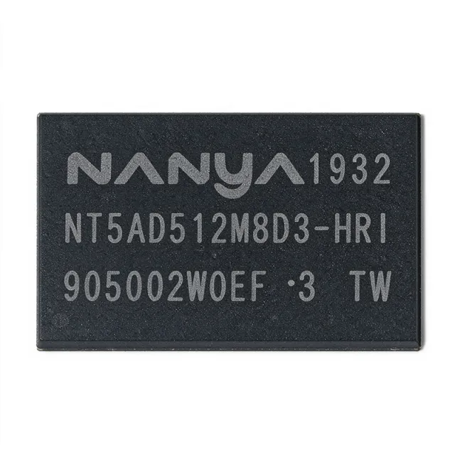
NT5AD512M16C4-HRI - 8Gb DDR4 SDRAM 512Mx16 | Nanya Technology
NT5AD512M16C4-HRI

NT5AD512M16C4-HRI - 8Gb DDR4 SDRAM 512Mx16 | Nanya Technology

The Nanya Technology NT5AD512M16C4-HRI is a high-performance DDR4 SDRAM device organized as 512M x 16, providing a total density of 8 Gigabits. It operates from a 1.2V power supply and is housed in a 96-pin TFBGA package, making it suitable for space-constrained applications requiring high memory bandwidth and low power consumption. DDR4 SDRAM (Double Data Rate 4 Synchronous Dynamic Random-Access Memory) is a type of volatile memory that transfers data on both edges of the clock signal, doubling the data rate compared to DDR3. It features a prefetch buffer of 8n, allowing high-speed data access while maintaining lower operating voltages (1.2V vs 1.5V for DDR3), which reduces power consumption and heat generation. DDR4 is the industry standard for modern computing, networking, and embedded systems, offering improved reliability and performance over previous generations. Key features of the NT5AD512M16C4-HRI include an industrial temperature grade (0°C to +95°C), auto self-refresh, built-in temperature sensor, auto precharge, asynchronous reset, data mask, write leveling, dynamic on-chip termination (ODT), ZQ calibration, and CRC (Cyclic Redundancy Check) function. These features enhance signal integrity, data reliability, and system robustness, particularly in demanding industrial environments. The device supports data rates up to 3200 MT/s (per the 'H' speed grade), with a CAS latency of 22 cycles. It utilizes a 16n prefetch architecture and includes on-die ECC for improved data integrity. The 96-ball TFBGA package measures 9mm x 13mm with a 0.8mm ball pitch, offering excellent thermal and electrical performance for high-speed operation. Typical applications include industrial controllers, embedded computing modules, networking equipment, and data storage systems. The industrial temperature range and robust feature set make it ideal for applications requiring reliable operation in harsh environments, such as factory automation, transportation, and outdoor infrastructure. When designing with this DDR4 device, ensure proper termination and layout practices are followed to maintain signal integrity at high speeds. The ZQ calibration pin requires a 240-ohm resistor to ground, and the VTT and VREF supplies must be properly decoupled. Refer to the Nanya datasheet for detailed PCB layout guidelines and timing parameters.

USD $45.94 במלאי
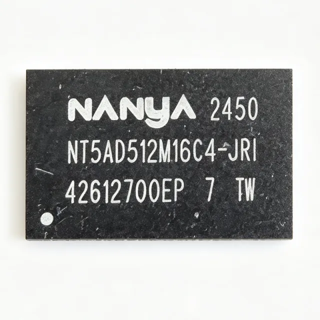
NT5AD512M16C4-JR - 8Gb DDR4-3200 SDRAM | Nanya Tech
NT5AD512M16C4-JR

NT5AD512M16C4-JR - 8Gb DDR4-3200 SDRAM | Nanya Tech

The Nanya Technology NT5AD512M16C4-JR is a high-speed, standard DDR4 SDRAM component organized as 512M x16, providing 8Gbit of memory density. It operates from a 1.2V power supply and supports data rates up to 1.6GHz (DDR4-3200), making it suitable for a wide range of computing, networking, and industrial applications. The device is housed in a 96-ball TFBGA package, offering a compact footprint for space-constrained PCB designs. DDR4 SDRAM (Double Data Rate 4 Synchronous Dynamic Random-Access Memory) is a type of volatile memory that transfers data on both edges of the clock signal, doubling the data rate compared to its predecessor DDR3. It is a key component in modern computing systems, providing the main memory for processors, and is also used in networking equipment, industrial controllers, and embedded systems. DDR4 operates at a lower voltage (1.2V) than DDR3 (1.5V), reducing power consumption and heat generation, which is critical for high-density memory modules and portable devices. Key features of the NT5AD512M16C4-JR include auto self-refresh, a built-in temperature sensor, auto precharge, asynchronous reset, data mask, write leveling, dynamic on-chip termination (DTC), ZQ calibration, and CRC (Cyclic Redundancy Check) function. These features enhance signal integrity, reliability, and ease of integration in high-speed systems. The operating temperature range is 0°C to +95°C, making it suitable for commercial and industrial environments. Technically, the device supports a burst length of 8 and on-die termination (ODT) for improved signal quality. The ZQ calibration function allows the device to adjust its output driver and ODT impedances to match the system's characteristic impedance, reducing reflections and improving data eye margins. The CRC function provides error detection for data transmitted during write operations, enhancing data integrity in critical applications. Typical applications include consumer electronics (e.g., set-top boxes, smart TVs), industrial automation, networking systems (routers, switches), and smart IoT devices. The high density and speed make it ideal for applications requiring large memory capacity and fast data throughput, such as edge computing and real-time data processing. When designing with this component, ensure proper decoupling capacitors are placed near the power pins to minimize noise, and follow the PCB layout guidelines in the datasheet for high-speed signals to maintain signal integrity. The device requires a 1.2V VDD and a separate VPP supply (2.5V) for the wordline driver, which must be properly regulated.

USD $73.75 צור קשר
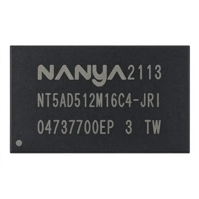
NT5AD512M16C4-JRI - 8Gb DDR4-3200 SDRAM | Nanya Technology
NT5AD512M16C4-JRI

NT5AD512M16C4-JRI - 8Gb DDR4-3200 SDRAM | Nanya Technology

The Nanya Technology NT5AD512M16C4-JRI is a high-performance DDR4 SDRAM device organized as 512M x 16 bits, providing 8Gb of memory density. It operates at a clock frequency of 1.6GHz (DDR4-3200) with a supply voltage of 1.2V, and is housed in a 96-ball TFBGA package. This component is designed for a wide range of computing and embedded applications, offering high-speed data transfer and low power consumption. DDR4 SDRAM (Double Data Rate 4 Synchronous Dynamic Random-Access Memory) is a type of volatile memory that transfers data on both edges of the clock signal, effectively doubling the data rate. It is the successor to DDR3 and provides higher bandwidth, lower operating voltage (1.2V vs 1.5V), and improved signal integrity through features like on-die termination (ODT) and write leveling. DDR4 is a critical component in modern computing systems, from servers and desktops to embedded and industrial applications. Key features of the NT5AD512M16C4-JRI include auto self-refresh, built-in temperature sensor, auto precharge, asynchronous reset, data mask, write leveling, dynamic on-chip termination, ZQ calibration, and CRC (Cyclic Redundancy Check) function. These features enhance reliability and performance in demanding environments. The device supports an operating temperature range of -40°C to +95°C, making it suitable for industrial applications. The NT5AD512M16C4-JRI utilizes advanced CMOS technology and a 96-ball TFBGA package, which offers excellent thermal and electrical performance. The built-in temperature sensor enables efficient thermal management, while the ZQ calibration ensures optimal signal integrity. The CRC function provides error detection for data integrity, which is crucial for mission-critical systems. Typical applications include data storage, firmware boot, embedded logging, industrial controllers, computing modules, and replacement sourcing. Its high density and speed make it ideal for networking equipment, servers, and high-performance embedded systems. The wide temperature range and robust feature set ensure reliable operation in harsh environments. When designing with this component, ensure proper decoupling capacitors are placed near the power pins to minimize noise. The ZQ pin requires a 240-ohm resistor to ground for calibration. Follow the DDR4 layout guidelines for signal integrity, including matched trace lengths and proper termination.

USD $75.58 במלאי
NT5CB256M16CP-DI - 4Gb DDR3L SDRAM 256Mx16 | Nanya
NT5CB256M16CP-DI

NT5CB256M16CP-DI - 4Gb DDR3L SDRAM 256Mx16 | Nanya

The Nanya NT5CB256M16CP-DI is a 4Gb DDR3L SDRAM organized as 256Mx16, operating at 1.35V (DDR3L) with a 96-ball TFBGA package. It supports data rates up to DDR3-1600 (800 MHz clock) and is designed for commercial, industrial, and automotive temperature ranges. This memory device features 8 internal banks, differential clock inputs, and programmable CAS latency (CL), write latency (CWL), and additive latency. It is compliant with JEDEC DDR3L standards and offers on-die termination (ODT) for signal integrity. DDR3L SDRAM is a type of dynamic random-access memory that operates at a lower voltage (1.35V) compared to standard DDR3 (1.5V), reducing power consumption by about 20% while maintaining similar performance. It is part of the DDR3 memory family, which uses double data rate architecture to transfer data on both edges of the clock. DDR3L is widely used in mobile, embedded, and industrial applications where power efficiency is critical. Key features include a 256Mx16 organization (4Gb density), 1.35V supply voltage, 96-ball TFBGA package, and support for data rates up to 1600 Mbps/pin. The device has a programmable CAS latency of 5-11, write latency of 5-9, and additive latency of 0-13. It also features 8 internal banks, differential clock inputs, and on-die termination. The operating temperature range is -40°C to +95°C (industrial) and -40°C to +105°C (automotive). The NT5CB256M16CP-DI uses a 70nm process technology, enabling high density and low power consumption. It incorporates DLL (delay-locked loop) for precise timing, and supports self-refresh and partial array self-refresh for power saving. The device is RoHS compliant and lead-free. Typical applications include embedded systems, networking equipment, industrial automation, automotive infotainment, and solid-state drives. Its low voltage and wide temperature range make it suitable for harsh environments. When designing with this memory, ensure proper decoupling capacitors near the power pins and follow the layout guidelines in the datasheet to minimize signal integrity issues. The device requires a stable 1.35V supply and reference voltage (VREF) for optimal operation.

RFQ צור קשר