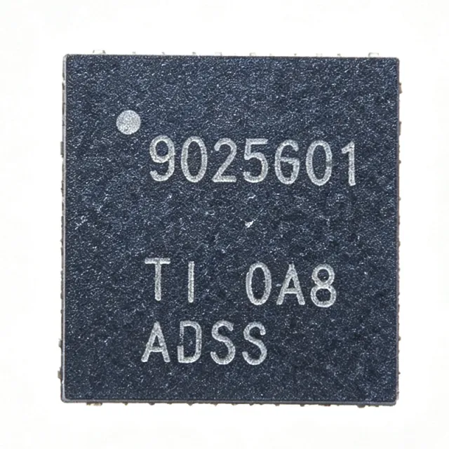
BQ25601RTWR - 3A I2C Buck Battery Charger | Texas Instruments
MPN: BQ25601RTWR ✓ פעיל| כמות | מחיר ליחידה | סה"כ |
|---|---|---|
| 1 | $1.02 | $1.02 |
| 10 | $0.92 | $9.20 |
| 100 | $0.75 | $75.00 |
| 500 | $0.58 | $290.00 |
| 1,000 | $0.46 | $460.00 |
BQ25601RTWR סקירה
A battery charger IC is a power management integrated circuit that regulates the charging of rechargeable batteries, ensuring safe and efficient charging while protecting the battery from overvoltage, overcurrent, and overtemperature conditions. Within the power management IC hierarchy, the BQ25601 integrates a synchronous buck converter, NVDC power path management, and an I2C interface, enabling dynamic power management between the input source, system load, and battery. This allows the system to boot and operate even when the battery is deeply discharged or absent.
Key features include a 3A fast-charge current, adjustable charge voltage from 3.856V to 4.624V, high input voltage support up to 13.5V, and an integrated bootstrap diode for the high-side gate drive that simplifies system design and reduces BOM count. The I2C serial interface provides programmable charge current, charge voltage, and input current limits, and supports On-The-Go (OTG) boost operation from the battery to power attached USB peripherals.
The BQ25601 uses a synchronous buck topology with a high-efficiency power stage, achieving approximately 92% efficiency at typical operating conditions. Input voltage and current regulation (DPM) deliver maximum charging power from USB adapters and other sources, while protections include input overvoltage, battery overvoltage, and thermal shutdown.
Typical applications include smartphones, tablets, portable speakers, power banks, and industrial or medical handheld devices requiring reliable high-current single-cell charging with power path management.
When designing with the BQ25601, ensure a proper PCB layout with thermal vias under the exposed pad and adequate copper area for heat dissipation at 3A charge currents, and configure I2C registers to set the desired charge parameters. According to TI datasheet (bq25601.pdf), pricing at authorized distributors starts around $0.37 at LCSC as of 2026-08-30.
חלופות תחליף ישיר עבור BQ25601RTWR — אותו מארז, תואם פין-לפין. חלקים במארז שונה הדורשים עיבוד מחדש של ה-PCB אינם נכללים.
כלי השוואה מהיר — בחרו חלקים חלופיים להשוואה זה לצד זה:
BQ25601RTWT
✅ Drop-In📋 חלופה להתייחסות (לא בקטלוג)
BQ25892RTWT
✅ Drop-In📋 חלופה להתייחסות (לא בקטלוג)
BQ25895RTWT
✅ Drop-In ⚠️ מפרטים לא מאומתים📋 חלופה להתייחסות (לא בקטלוג)
BQ25601QRTWRQ1
✅ Drop-In ⚠️ מפרטים לא מאומתיםצור קשר לקבלת מחיר
הצג גיליון נתונים ←BQ25896RTWT
✅ Drop-In ⚠️ מפרטים לא מאומתים📋 חלופה להתייחסות (לא בקטלוג)
BQ25601RTWR מפרטים
| פונקציה | Single-cell Li-Ion/Li-Polymer buck battery charger with NVDC power path |
| Chemistry | Li-Ion / Li-Polymer |
| Maximum Charge Current | 3 A |
| טווח מתח כניסה | 3.9 V to 13.5 V |
| Absolute Maximum Input Voltage | 14 V |
| Charge Voltage Range | 3.856 V to 4.624 V |
| Series Cells | 1 |
| Control Interface | I2C |
| Power Path Management | NVDC (Narrow VDC) |
| OTG Boost Mode | Yes |
| Integrated Bootstrap Diode | Yes |
| טמפרטורת פעולה | -40C to +85C |
| מארז | 24-WQFN (4x4 mm) RTW with exposed pad |
| סוג הרכבה | Surface Mount |
| סטטוס RoHS | Compliant |
תצורת פינים של BQ25601RTWR
| פין 1 | BTST — Bootstrap for high-side gate driver (internal diode from REGN) |
| פין 2 | REGN — LDO output for gate drive, 5V typical |
| פין 3 | OTG — OTG mode enable input |
| פין 4 | ACOK — Input source indication open-drain output |
| פין 5 | I2C SCL — I2C clock input |
| פין 6 | SDA — I2C data input/output |
| פין 7 | INT — Interrupt open-drain output |
| פין 8 | STAT — Charge status indication output |
| פין 9 | PGND — Power ground |
| פין 10 | SW — Switching node of buck converter |
| פין 11 | BAT — Battery connection / sense |
| פין 12 | SYS — NVDC system output |
| פין 13 | CS — [DATA_NEEDED: exact pin name] |
| פין 14 | ACN — [DATA_NEEDED: exact pin name] |
| פין 15 | ACP — [DATA_NEEDED: exact pin name] |
| פין 16 | VAC — Input voltage sense / supply |
| פין 17 | DSEL — [DATA_NEEDED: exact pin name] |
| פין 18 | ILIM — [DATA_NEEDED: exact pin name] |
| פין 19 | TS — Battery temperature sensing via NTC |
| פין 20 | AGND — Analog ground |
יישומים טיפוסיים
BQ25601RTWR מתאים עבור 6 יישוםs: Smartphone Fast Charging, Tablets and e-Readers, Power Banks with OTG Output, Portable Bluetooth Speakers, Industrial Handheld Devices, Medical Portable Diagnostics.
Smartphone Fast Charging
The BQ25601RTWR is ideal for smartphone charging because its 3A fast-charge current and 3.9V-13.5V input range support both 5V standard and 9V-class adapters. The NVDC power path lets the phone boot instantly even with a fully depleted battery, while input current DPM prevents adapter overload. With approximately 92% buck efficiency and an integrated bootstrap diode, it reduces BOM count and thermal load in dense handset layouts.
מומלץ
Tablets and e-Readers
Tablets benefit from the BQ25601's 3A charge capability, which refills large single-cell packs quickly, and its 4.624V maximum charge voltage covering high-capacity Li-Polymer cells. NVDC power path management guarantees stable system voltage during simultaneous charging and operation. The I2C interface lets the application processor dynamically adjust charge current based on thermal conditions, and OTG mode powers accessories from the battery at 5V-class output.
מומלץ
Power Banks with OTG Output
In power banks, the BQ25601RTWR handles both charging from USB adapters and OTG boost discharge to 5V output from the battery, all in one IC. The 13.5V input limit accepts multi-voltage adapter inputs, while 3A charging shortens recharge time of the internal pack. The I2C register set enables LED-indicated state-of-charge management and automatic switchover between adapter and battery power without external switchover circuitry.
מומלץ
Portable Bluetooth Speakers
Battery-powered speakers use the BQ25601RTWR's NVDC power path so audio amplifiers receive a regulated system rail regardless of battery sag during high-current playback. The 3A charge current minimizes recharge downtime, and OTG mode can power USB accessories. Thermal shutdown and battery overvoltage protection protect the pack during charging inside acoustically sealed enclosures with limited airflow, a common constraint in speaker industrial design.
מומלץ
Industrial Handheld Devices
Industrial scanners, meters, and data loggers charge from varied adapters, and the BQ25601's wide 3.9V-13.5V input plus input overvoltage protection tolerates noisy or miswired supplies. The -40C to +85C operating range suits harsh environments, and I2C telemetry (charge status, fault registers) lets the host MCU report battery health. NVDC power path ensures uptime during battery swap, which is critical for continuous data collection in the field.
מומלץ
Medical Portable Diagnostics
Portable medical instruments require predictable charging and uninterrupted operation; the BQ25601RTWR provides both. Its programmable 3.856V-4.624V charge voltage supports medical-grade cell requirements, and NVDC power path maintains a clean regulated system rail for sensitive analog front-ends during charging. The I2C interface allows firmware-controlled charge termination criteria, and built-in overvoltage and thermal protections support the safety requirements of handheld diagnostic and monitoring devices.
מומלץ
סיכום מוצרים מומלצים
נתוני עזר הנדסיים עבור BQ25601RTWR — השוואה, הנחיות תכנון ומידע על תאימות.
מדריך בחירה
השוואה עם חלופות
| פרמטר | מוצר זה | BQ25601RTWT | BQ25892RTWT | BQ25895RTWT | BQ25601QRTWRQ1 |
|---|---|---|---|---|---|
| Package | 24-WQFN (4x4 mm) | 24-WQFN (4x4 mm) - same | 24-WQFN (4x4 mm) - same | 24-WQFN (4x4 mm) - same | 24-WQFN (4x4 mm) - same |
| Brand | Texas Instruments | Texas Instruments | Texas Instruments | Texas Instruments | Texas Instruments |
| Max Charge Current | 3 A | 3 A | 3 A (higher OTG discharge) | 5 A | 3 A |
| Max Input Voltage | 13.5 V | 13.5 V | 14 V | 14 V | 13.5 V |
| Charge Voltage Range | 3.856 V to 4.624 V | 3.856 V to 4.624 V | 3.84 V to 4.624 V | 3.84 V to 4.624 V | 3.856 V to 4.624 V |
| Interface | I2C | I2C (identical register map) | I2C (different registers) | I2C (different registers) | I2C (similar registers) |
| NVDC Power Path + OTG | Yes / Yes | Yes / Yes | Yes / Yes | Yes / Yes | Yes / Yes |
| Automotive AEC-Q100 | No | No | No | No | Yes |
מבדילים עיקריים
- Integrated bootstrap diode (לעומתBQ25892RTWT)
- True drop-in twin availability (לעומתBQ25601RTWT)
- Lower cost than higher-current family parts (לעומתBQ25895RTWT)
הערות תכנון
At 3A charge current with a large input-to-battery delta (e.g., 12V input to 4V battery), conduction and switching losses concentrate in the 4x4mm QFN exposed pad. Provide a solid ground plane with at least a 5x5 array of thermal vias (0.3mm drill) under the pad to keep junction temperature within limits at 85C ambient. TI's BQ25601 EVM layout is a proven starting reference.
Keep the SW node, BTST, and input loop as compact as possible: place the input capacitor within 2mm of ACP/ACN and VAC, and the inductor close to SW. Separate AGND and PGND planes, joining at a single star point under the IC. Route I2C (SCL/SDA) away from the SW node to avoid register corruption from switching noise.
Always connect the TS pin to a 10k NTC (or fixed divider) - floating TS can block charging due to temperature fault. When migrating to BQ25892, remember the I2C register maps differ even though the pinout is identical (per TI E2E forum); update firmware before powering up. Observe the 14V absolute maximum input; add input TVS for adapters without OVP.
מידע על תאימות
RoHS compliant per DigiKey product listing (Charger IC Lithium Ion/Polymer, 24-WQFN). Not AEC-Q100 qualified - choose BQ25601QRTWRQ1 for automotive. REACH and halogen-free status per TI quality pages.




