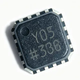
CDCLVP110VFR - 1:10 LVPECL/HSTL Clock Driver | Texas Instruments
MPN: CDCLVP110VFR ✓ פעילCDCLVP110VFR סקירה
A clock driver is an integrated circuit that buffers and distributes clock signals to multiple loads while maintaining signal integrity and minimizing skew. It sits between a clock source, such as an oscillator or PLL, and the downstream components that require synchronized timing. Clock drivers are essential in high-speed digital systems where precise timing is critical, such as data converters, FPGAs, and networking equipment.
Key features of the CDCLVP110VFR include a 2:10 configuration (two inputs, ten outputs), support for LVPECL and HSTL input standards, and fully compatible outputs with LVECL/LVPECL/HSTL logic levels. The device operates from a single supply voltage, simplifying power design. It is characterized for operation from -40°C to 85°C, making it suitable for industrial environments.
The CDCLVP110VFR uses a differential input structure to reject common-mode noise, ensuring clean clock distribution even in noisy environments. The selectable input multiplexer allows the user to choose between two clock sources, providing redundancy or frequency selection. The outputs are designed to drive 50-ohm transmission lines, and the device includes a VBB reference voltage output for single-ended input operation, though differential mode is recommended for high-speed performance.
Typical applications include clock distribution for high-speed ADCs/DACs, FPGA and ASIC clocking, networking switches and routers, and test and measurement equipment. The device's low skew and high frequency capability make it ideal for systems requiring synchronized multi-channel operation.
When designing with the CDCLVP110VFR, ensure proper termination of the differential outputs and bypass the power supply pins with decoupling capacitors. For single-ended input, connect the VBB pin to CLK0 with a 10-nF bypass capacitor to ground. For optimal performance up to 3.5 GHz, use differential mode.
חלופות תחליף ישיר עבור CDCLVP110VFR — אותו מארז, תואם פין-לפין. חלקים במארז שונה הדורשים עיבוד מחדש של ה-PCB אינם נכללים.
CDCLVP110VF
✅ Drop-In📋 חלופה להתייחסות (לא בקטלוג)
CDCLVP111VFR
✅ Drop-In ⚠️ מפרטים לא מאומתים📋 חלופה להתייחסות (לא בקטלוג)
CDCLVP110VFR מפרטים
| פונקציה | Clock Fanout Buffer (Distribution), Multiplexer |
| Configuration | 2:10 |
| Maximum Frequency | 3.5 GHz |
| Input Type | LVPECL, HSTL |
| סוג פלט | LVPECL |
| מספר יציאות | 10 (differential pairs) |
| מתח אספקה | 2.375 V to 3.8 V |
| טווח טמפרטורת פעולה | -40°C to 85°C |
| מארז | 32-LQFP |
| סוג הרכבה | Surface Mount |
| Input Multiplexer | Yes (selectable) |
| VBB Reference Voltage Output | Yes |
| סטטוס RoHS | Compliant |
תצורת פינים של CDCLVP110VFR
| פין 1 | Q0 — Differential output 0 (positive) |
| פין 2 | Q0# — Differential output 0 (negative) |
| פין 3 | Q1 — Differential output 1 (positive) |
| פין 4 | Q1# — Differential output 1 (negative) |
| פין 5 | Q2 — Differential output 2 (positive) |
| פין 6 | Q2# — Differential output 2 (negative) |
| פין 7 | Q3 — Differential output 3 (positive) |
| פין 8 | Q3# — Differential output 3 (negative) |
| פין 9 | Q4 — Differential output 4 (positive) |
| פין 10 | Q4# — Differential output 4 (negative) |
| פין 11 | Q5 — Differential output 5 (positive) |
| פין 12 | Q5# — Differential output 5 (negative) |
| פין 13 | Q6 — Differential output 6 (positive) |
| פין 14 | Q6# — Differential output 6 (negative) |
| פין 15 | Q7 — Differential output 7 (positive) |
| פין 16 | Q7# — Differential output 7 (negative) |
| פין 17 | Q8 — Differential output 8 (positive) |
| פין 18 | Q8# — Differential output 8 (negative) |
| פין 19 | Q9 — Differential output 9 (positive) |
| פין 20 | Q9# — Differential output 9 (negative) |
| פין 21 | VCC — Power supply |
| פין 22 | GND — Ground |
| פין 23 | CLK0 — Input clock 0 (positive) |
| פין 24 | CLK0# — Input clock 0 (negative) |
| פין 25 | CLK1 — Input clock 1 (positive) |
| פין 26 | CLK1# — Input clock 1 (negative) |
| פין 27 | SEL — Input select |
| פין 28 | VBB — Reference voltage output |
| פין 29 | NC — No connect |
| פין 30 | NC — No connect |
| פין 31 | NC — No connect |
| פין 32 | NC — No connect |
יישומים טיפוסיים
CDCLVP110VFR מתאים עבור 6 יישוםs: High-Speed ADC/DAC Clock Distribution, FPGA and ASIC Clocking, Networking and Communications, Test and Measurement Equipment, Broadcast Video and Audio, Industrial Automation and Control.
High-Speed ADC/DAC Clock Distribution
The CDCLVP110VFR provides low-skew, high-frequency clock distribution for high-speed data converters. Its 3.5 GHz capability and differential LVPECL outputs ensure precise timing for ADCs and DACs, improving signal integrity and reducing aperture jitter. The selectable input multiplexer allows interfacing with various clock sources, and the low output skew ensures synchronized sampling across multiple channels.
מומלץ
FPGA and ASIC Clocking
The CDCLVP110VFR fans out a single clock to multiple FPGA or ASIC clock inputs, ensuring synchronized operation. Its low skew and high frequency support high-performance logic designs. The differential outputs are compatible with FPGA clock pins, and the wide supply voltage range allows integration with various FPGA power domains. The device's industrial temperature range makes it suitable for rugged applications.
מומלץ
Networking and Communications
In networking switches and routers, the CDCLVP110VFR distributes high-speed clocks to PHYs, MACs, and switch fabrics. Its 3.5 GHz frequency supports 10GbE and beyond, while the low skew ensures synchronized data transmission. The selectable input allows redundancy, and the LVPECL outputs drive long traces with minimal distortion. The device's small LQFP package saves board space in dense line cards.
מומלץ
Test and Measurement Equipment
The CDCLVP110VFR is used in oscilloscopes, signal generators, and logic analyzers to distribute precise timing references. Its high frequency and low skew ensure accurate timebase generation. The differential outputs provide clean signals to multiple measurement channels, and the selectable input allows switching between internal and external references. The industrial temperature range ensures stable operation in lab and field environments.
מומלץ
Broadcast Video and Audio
The CDCLVP110VFR distributes clock signals in broadcast video routers and audio mixing consoles. Its low jitter and high frequency support high-definition video formats and high-sample-rate audio. The differential outputs drive long cable runs with minimal signal degradation. The selectable input allows synchronization to external references, and the wide supply voltage range accommodates various power architectures.
מומלץ
Industrial Automation and Control
The CDCLVP110VFR provides reliable clock distribution in industrial controllers and PLCs. Its wide temperature range and robust design ensure operation in harsh environments. The selectable input allows redundancy, and the low skew ensures synchronized control loops. The device's small package is suitable for space-constrained control modules, and its low power consumption reduces thermal stress.
מומלץ
סיכום מוצרים מומלצים
נתוני עזר הנדסיים עבור CDCLVP110VFR — השוואה, הנחיות תכנון ומידע על תאימות.
מדריך בחירה
השוואה עם חלופות
| פרמטר | מוצר זה | CDCLVP110VF | CDCLVP111VFR | CDCLVP111RHBR |
|---|---|---|---|---|
| Package | 32-LQFP | 32-LQFP | 32-LQFP | VQFN-32 |
| Brand | Texas Instruments | Texas Instruments | Texas Instruments | Texas Instruments |
| Configuration | 2:10 | 2:10 | 1:10 | 1:10 |
| Maximum Frequency | 3.5 GHz | 3.5 GHz | 3.5 GHz | 3.5 GHz |
| Input Type | LVPECL, HSTL | LVPECL, HSTL | LVPECL, HSTL | LVPECL, HSTL |
| Output Type | LVPECL | LVPECL | LVPECL | LVPECL |
| Supply Voltage | 2.375 V to 3.8 V | 2.375 V to 3.8 V | 2.375 V to 3.8 V | 2.375 V to 3.8 V |
| Operating Temperature | -40°C to 85°C | -40°C to 85°C | -40°C to 85°C | -40°C to 85°C |
מבדילים עיקריים
- Higher frequency capability (לעומתCDCLVP111VFR)
- Selectable input multiplexer (לעומתCDCLVP111VFR)
- Tape-and-reel packaging (לעומתCDCLVP110VF)
הערות תכנון
For high-speed operation up to 3.5 GHz, use controlled impedance traces (50 ohms single-ended, 100 ohms differential) for all clock inputs and outputs. Keep traces as short as possible and avoid vias to minimize signal degradation. Place the device close to the clock source and loads.
Bypass the VCC pin with a 0.1 uF ceramic capacitor placed as close to the pin as possible, and a 10 uF bulk capacitor nearby. Use a low-inductance ground plane to minimize noise. The device operates from 2.375 V to 3.8 V, so ensure the supply is clean and stable.
For single-ended input operation, connect the VBB pin to CLK0 and bypass it to GND with a 10-nF capacitor. However, for frequencies above 1 GHz, differential mode is strongly recommended to maintain signal integrity. Do not leave unused inputs floating; tie them to appropriate levels.
מידע על תאימות
RoHS compliant per TI product page. No AEC-Q100 qualification indicated.