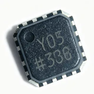
CDCLVP110VFR - 1:10 LVPECL/HSTL Clock Driver | Texas Instruments
MPN: CDCLVP110VFR ✓ Hoạt độngCDCLVP110VFR Tóm tắt
A clock driver is an integrated circuit that buffers and distributes clock signals to multiple loads while maintaining signal integrity and minimizing skew. It sits between a clock source, such as an oscillator or PLL, and the downstream components that require synchronized timing. Clock drivers are essential in high-speed digital systems where precise timing is critical, such as data converters, FPGAs, and networking equipment.
Key features of the CDCLVP110VFR include a 2:10 configuration (two inputs, ten outputs), support for LVPECL and HSTL input standards, and fully compatible outputs with LVECL/LVPECL/HSTL logic levels. The device operates from a single supply voltage, simplifying power design. It is characterized for operation from -40°C to 85°C, making it suitable for industrial environments.
The CDCLVP110VFR uses a differential input structure to reject common-mode noise, ensuring clean clock distribution even in noisy environments. The selectable input multiplexer allows the user to choose between two clock sources, providing redundancy or frequency selection. The outputs are designed to drive 50-ohm transmission lines, and the device includes a VBB reference voltage output for single-ended input operation, though differential mode is recommended for high-speed performance.
Typical applications include clock distribution for high-speed ADCs/DACs, FPGA and ASIC clocking, networking switches and routers, and test and measurement equipment. The device's low skew and high frequency capability make it ideal for systems requiring synchronized multi-channel operation.
When designing with the CDCLVP110VFR, ensure proper termination of the differential outputs and bypass the power supply pins with decoupling capacitors. For single-ended input, connect the VBB pin to CLK0 with a 10-nF bypass capacitor to ground. For optimal performance up to 3.5 GHz, use differential mode.
Bộ thay thế dễ dàng lắp đặt cho CDCLVP110VFR — cùng gói, chân-to-chân tương thích. Các bộ phận yêu cầu hàn PCB bị loại trừ.
CDCLVP110VF
✅ Drop-In📋 Tham chiếu thay thế (không có trong danh mục)
CDCLVP111VFR
✅ Drop-In ⚠️ Thông số chưa được xác minh📋 Tham chiếu thay thế (không có trong danh mục)
CDCLVP110VFR Thông số kỹ thuật
| Chức năng | Clock Fanout Buffer (Distribution), Multiplexer |
| Configuration | 2:10 |
| Maximum Frequency | 3.5 GHz |
| Input Type | LVPECL, HSTL |
| Kiểu đầu ra | LVPECL |
| Số lượng đầu ra | 10 (differential pairs) |
| Điện áp cung cấp | 2.375 V to 3.8 V |
| Khoảng nhiệt độ hoạt động | -40°C to 85°C |
| Hộp | 32-LQFP |
| Kiểu lắp đặt | Surface Mount |
| Input Multiplexer | Yes (selectable) |
| VBB Reference Voltage Output | Yes |
| Trạng thái RoHS | Compliant |
Cấu hình chân CDCLVP110VFR
| Chân 1 | Q0 — Differential output 0 (positive) |
| Chân 2 | Q0# — Differential output 0 (negative) |
| Chân 3 | Q1 — Differential output 1 (positive) |
| Chân 4 | Q1# — Differential output 1 (negative) |
| Chân 5 | Q2 — Differential output 2 (positive) |
| Chân 6 | Q2# — Differential output 2 (negative) |
| Chân 7 | Q3 — Differential output 3 (positive) |
| Chân 8 | Q3# — Differential output 3 (negative) |
| Chân 9 | Q4 — Differential output 4 (positive) |
| Chân 10 | Q4# — Differential output 4 (negative) |
| Chân 11 | Q5 — Differential output 5 (positive) |
| Chân 12 | Q5# — Differential output 5 (negative) |
| Chân 13 | Q6 — Differential output 6 (positive) |
| Chân 14 | Q6# — Differential output 6 (negative) |
| Chân 15 | Q7 — Differential output 7 (positive) |
| Chân 16 | Q7# — Differential output 7 (negative) |
| Chân 17 | Q8 — Differential output 8 (positive) |
| Chân 18 | Q8# — Differential output 8 (negative) |
| Chân 19 | Q9 — Differential output 9 (positive) |
| Chân 20 | Q9# — Differential output 9 (negative) |
| Chân 21 | VCC — Power supply |
| Chân 22 | GND — Ground |
| Chân 23 | CLK0 — Input clock 0 (positive) |
| Chân 24 | CLK0# — Input clock 0 (negative) |
| Chân 25 | CLK1 — Input clock 1 (positive) |
| Chân 26 | CLK1# — Input clock 1 (negative) |
| Chân 27 | SEL — Input select |
| Chân 28 | VBB — Reference voltage output |
| Chân 29 | NC — No connect |
| Chân 30 | NC — No connect |
| Chân 31 | NC — No connect |
| Chân 32 | NC — No connect |
Ứng dụng tiêu biểu
CDCLVP110VFR phù hợp cho 6 Áp dụngs: High-Speed ADC/DAC Clock Distribution, FPGA and ASIC Clocking, Networking and Communications, Test and Measurement Equipment, Broadcast Video and Audio, Industrial Automation and Control.
High-Speed ADC/DAC Clock Distribution
The CDCLVP110VFR provides low-skew, high-frequency clock distribution for high-speed data converters. Its 3.5 GHz capability and differential LVPECL outputs ensure precise timing for ADCs and DACs, improving signal integrity and reducing aperture jitter. The selectable input multiplexer allows interfacing with various clock sources, and the low output skew ensures synchronized sampling across multiple channels.
Được đề xuất
FPGA and ASIC Clocking
The CDCLVP110VFR fans out a single clock to multiple FPGA or ASIC clock inputs, ensuring synchronized operation. Its low skew and high frequency support high-performance logic designs. The differential outputs are compatible with FPGA clock pins, and the wide supply voltage range allows integration with various FPGA power domains. The device's industrial temperature range makes it suitable for rugged applications.
Được đề xuất
Networking and Communications
In networking switches and routers, the CDCLVP110VFR distributes high-speed clocks to PHYs, MACs, and switch fabrics. Its 3.5 GHz frequency supports 10GbE and beyond, while the low skew ensures synchronized data transmission. The selectable input allows redundancy, and the LVPECL outputs drive long traces with minimal distortion. The device's small LQFP package saves board space in dense line cards.
Được đề xuất
Test and Measurement Equipment
The CDCLVP110VFR is used in oscilloscopes, signal generators, and logic analyzers to distribute precise timing references. Its high frequency and low skew ensure accurate timebase generation. The differential outputs provide clean signals to multiple measurement channels, and the selectable input allows switching between internal and external references. The industrial temperature range ensures stable operation in lab and field environments.
Được đề xuất
Broadcast Video and Audio
The CDCLVP110VFR distributes clock signals in broadcast video routers and audio mixing consoles. Its low jitter and high frequency support high-definition video formats and high-sample-rate audio. The differential outputs drive long cable runs with minimal signal degradation. The selectable input allows synchronization to external references, and the wide supply voltage range accommodates various power architectures.
Được đề xuất
Industrial Automation and Control
The CDCLVP110VFR provides reliable clock distribution in industrial controllers and PLCs. Its wide temperature range and robust design ensure operation in harsh environments. The selectable input allows redundancy, and the low skew ensures synchronized control loops. The device's small package is suitable for space-constrained control modules, and its low power consumption reduces thermal stress.
Được đề xuất
Tóm tắt các sản phẩm được đề xuất
Dữ liệu tham khảo kỹ thuật cho CDCLVP110VFR — so sánh, hướng dẫn thiết kế và thông tin tuân thủ.
Hướng dẫn chọn lựa
So sánh với các sản phẩm thay thế
| Tham số | Sản phẩm này | CDCLVP110VF | CDCLVP111VFR | CDCLVP111RHBR |
|---|---|---|---|---|
| Package | 32-LQFP | 32-LQFP | 32-LQFP | VQFN-32 |
| Brand | Texas Instruments | Texas Instruments | Texas Instruments | Texas Instruments |
| Configuration | 2:10 | 2:10 | 1:10 | 1:10 |
| Maximum Frequency | 3.5 GHz | 3.5 GHz | 3.5 GHz | 3.5 GHz |
| Input Type | LVPECL, HSTL | LVPECL, HSTL | LVPECL, HSTL | LVPECL, HSTL |
| Output Type | LVPECL | LVPECL | LVPECL | LVPECL |
| Supply Voltage | 2.375 V to 3.8 V | 2.375 V to 3.8 V | 2.375 V to 3.8 V | 2.375 V to 3.8 V |
| Operating Temperature | -40°C to 85°C | -40°C to 85°C | -40°C to 85°C | -40°C to 85°C |
Bảo phân biệt quan trọng
- Higher frequency capability (vsCDCLVP111VFR)
- Selectable input multiplexer (vsCDCLVP111VFR)
- Tape-and-reel packaging (vsCDCLVP110VF)
Ghi chú thiết kế
For high-speed operation up to 3.5 GHz, use controlled impedance traces (50 ohms single-ended, 100 ohms differential) for all clock inputs and outputs. Keep traces as short as possible and avoid vias to minimize signal degradation. Place the device close to the clock source and loads.
Bypass the VCC pin with a 0.1 uF ceramic capacitor placed as close to the pin as possible, and a 10 uF bulk capacitor nearby. Use a low-inductance ground plane to minimize noise. The device operates from 2.375 V to 3.8 V, so ensure the supply is clean and stable.
For single-ended input operation, connect the VBB pin to CLK0 and bypass it to GND with a 10-nF capacitor. However, for frequencies above 1 GHz, differential mode is strongly recommended to maintain signal integrity. Do not leave unused inputs floating; tie them to appropriate levels.
Thông tin tuân thủ
RoHS compliant per TI product page. No AEC-Q100 qualification indicated.