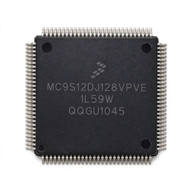
MC9S12DJ128CPVE - HCS12 16-bit MCU, 128KB Flash, 112-LQFP | NXP
MPN: MC9S12DJ128CPVE ✗ Akhir HidupMC9S12DJ128CPVE Ringkasan
A 16-bit microcontroller (MCU) is a programmable processor with an internal data path of 16 bits, providing a balance between the simplicity of 8-bit devices and the computational throughput of 32-bit cores. Within the broader taxonomy, the MC9S12DJ128CPVE sits under HCS12 -> 16-bit MCU -> microcontroller -> embedded processor -> semiconductor. It is widely used in automotive body electronics, industrial control, and consumer appliances where deterministic real-time response, on-chip analog peripherals, and CAN connectivity are valued.
Key features include two asynchronous serial communications interfaces (SCI), two synchronous serial peripheral interfaces (SPI), one Inter-IC (I2C) bus interface, an 8-channel IC/OC enhanced capture timer, two 8-channel 10-bit analog-to-digital converters (ADC), an 8-channel pulse-width modulator (PWM), and 20 discrete digital I/O lines. The HCS12 core integrates the standard S12 instruction set with background debug mode (BDM) and on-chip interrupt control.
The architecture combines a 16-bit RISC-like programming model with a rich set of mixed-signal peripherals. The dual 10-bit ADC, 8-channel PWM, and CAN-compatible timers enable the part to replace multiple external components in motor-control and sensor-interface designs. System resource mapping, clock generation, interrupt control, and bus interfacing are all handled on-chip, simplifying board layout.
Typical applications include automotive body controllers, HVAC control modules, instrument clusters, industrial CAN nodes, and battery management peripherals. Its wide operating voltage range and automotive temperature grade make it suitable for under-hood and chassis deployments, while the LQFP-112 footprint allows conventional SMT assembly.
When designing with the MC9S12DJ128CPVE, engineers should review the NRND notice on the NXP product page and plan a migration path. The S12X and S12 MagniV families offer pin-compatible successors with additional memory and CAN FD support. Verify supply-chain availability before committing to new designs.
Alternatif penggantian untuk MC9S12DJ128CPVE — paket yang sama, pin-pada-pin kompatibel. Bagian paket yang berbeda memerlukan kerja ulang PCB diabaikan.
Variasi di dalam seri ini
Model-series yang sama yang kompatibel dengan penggantian MC9S12DJ128CPVE (sama faktor bentuk dan footprint) — berbeda di dalam Package, Flash Memory, Product Type, ADC, Architecture.
MC9S12DJ128MPVE
Kontak untuk harga
Lihat Datasheet →MC9S12DT256CPVE
Kontak untuk harga
Lihat Datasheet →MC9S12DP512CPVE
Kontak untuk harga
Lihat Datasheet →MC9S12DT256VPVE
Kontak untuk harga
Lihat Datasheet →MC9S12H256VFVE
Kontak untuk harga
Lihat Datasheet →MC9S12DJ128CPVE Rating Maksimal & Karakteristik Listrik
| Core | HCS12 |
| Lebar Bus Data | 16 bit |
| Frekuensi Bawah Maximum | 25 MHz |
| Program Memory Size | 128 KB (128K x 8) Flash |
| Paket | 112-LQFP (20 x 20 mm) |
| Tipe Mounting | Surface Mount |
| SCI (UART) Interfaces | 2 |
| SPI Interfaces | 2 |
| I2C (Inter-IC Bus) Interfaces | 1 |
| ADC Channels | 2 x 8-channel, 10-bit |
| PWM Channels | 8 |
| Enhanced Capture Timer Channels | 8 (IC/OC) |
| Digital I/O Pins | 20 |
| Status Lingkungan Hidup | NRND (Not Recommended for New Designs) |
Konfigurasi Pin MC9S12DJ128CPVE
| Pin produk 1 | TCLK — Timer clock input |
| Pin produk 2 | TDDR — Test / reserved signal |
| Pin produk 3 | BKGD — Background Debug Mode pin |
| Pin produk 4 | RESET — External reset input |
| Pin produk 5 | VDDR — Voltage regulator supply |
| Pin produk 6 | VDD — Digital supply voltage |
| Pin produk 7 | VSS — Digital ground |
| Pin produk 8 | VSS — Digital ground |
| Pin produk 9 | VDDPLL — PLL supply voltage |
| Pin produk 10 | VSSPLL — PLL ground |
| Pin produk 11 | PAD0 — Port AD bit 0 (digital I/O) |
| Pin produk 12 | PAD1 — Port AD bit 1 (digital I/O) |
| Pin produk 13 | PAD2 — Port AD bit 2 (digital I/O) |
| Pin produk 14 | PAD3 — Port AD bit 3 (digital I/O) |
| Pin produk 15 | PAD4 — Port AD bit 4 (digital I/O) |
| Pin produk 16 | PAD5 — Port AD bit 5 (digital I/O) |
| Pin produk 17 | PAD6 — Port AD bit 6 (digital I/O) |
| Pin produk 18 | PAD7 — Port AD bit 7 (digital I/O) |
| Pin produk 19 | PAD8 — Port AD bit 8 (digital I/O) |
| Pin produk 20 | PAD9 — Port AD bit 9 (digital I/O) |
| Pin produk 21 | PAD10 — Port AD bit 10 (digital I/O) |
| Pin produk 22 | PAD11 — Port AD bit 11 (digital I/O) |
| Pin produk 23 | PAD12 — Port AD bit 12 (digital I/O) |
| Pin produk 24 | PAD13 — Port AD bit 13 (digital I/O) |
| Pin produk 25 | PAD14 — Port AD bit 14 (digital I/O) |
| Pin produk 26 | PAD15 — Port AD bit 15 (digital I/O) |
| Pin produk 27 | PA0 — Port A bit 0 |
| Pin produk 28 | PA1 — Port A bit 1 |
| Pin produk 29 | PA2 — Port A bit 2 |
| Pin produk 30 | PA3 — Port A bit 3 |
| Pin produk 31 | PA4 — Port A bit 4 |
| Pin produk 32 | PA5 — Port A bit 5 |
| Pin produk 33 | PA6 — Port A bit 6 |
| Pin produk 34 | PA7 — Port A bit 7 |
| Pin produk 35 | PB0 — Port B bit 0 |
| Pin produk 36 | PB1 — Port B bit 1 |
| Pin produk 37 | PB2 — Port B bit 2 |
| Pin produk 38 | PB3 — Port B bit 3 |
| Pin produk 39 | PB4 — Port B bit 4 |
| Pin produk 40 | PB5 — Port B bit 5 |
| Pin produk 41 | PB6 — Port B bit 6 |
| Pin produk 42 | PB7 — Port B bit 7 |
| Pin produk 43 | PE0 — Port E bit 0 / IRQ |
| Pin produk 44 | PE1 — Port E bit 1 / IRQ |
| Pin produk 45 | PE2 — Port E bit 2 |
| Pin produk 46 | PE3 — Port E bit 3 |
| Pin produk 47 | PE4 — Port E bit 4 |
| Pin produk 48 | PE5 — Port E bit 5 |
| Pin produk 49 | PE6 — Port E bit 6 |
| Pin produk 50 | PE7 — Port E bit 7 |
| Pin produk 51 | PH0 — Port H bit 0 |
| Pin produk 52 | PH1 — Port H bit 1 |
| Pin produk 53 | PH2 — Port H bit 2 |
| Pin produk 54 | PH3 — Port H bit 3 |
| Pin produk 55 | PH4 — Port H bit 4 |
| Pin produk 56 | PH5 — Port H bit 5 |
| Pin produk 57 | PH6 — Port H bit 6 |
| Pin produk 58 | PH7 — Port H bit 7 |
| Pin produk 59 | PJ0 — Port J bit 0 |
| Pin produk 60 | PJ1 — Port J bit 1 |
| Pin produk 61 | PJ2 — Port J bit 2 |
| Pin produk 62 | PJ3 — Port J bit 3 |
| Pin produk 63 | PJ4 — Port J bit 4 |
| Pin produk 64 | PJ5 — Port J bit 5 |
| Pin produk 65 | PJ6 — Port J bit 6 |
| Pin produk 66 | PJ7 — Port J bit 7 |
| Pin produk 67 | PK0 — Port K bit 0 |
| Pin produk 68 | PK1 — Port K bit 1 |
| Pin produk 69 | PK2 — Port K bit 2 |
| Pin produk 70 | PK3 — Port K bit 3 |
| Pin produk 71 | PK4 — Port K bit 4 |
| Pin produk 72 | PK5 — Port K bit 5 |
| Pin produk 73 | PK6 — Port K bit 6 |
| Pin produk 74 | PK7 — Port K bit 7 |
| Pin produk 75 | PM0 — Port M bit 0 |
| Pin produk 76 | PM1 — Port M bit 1 |
| Pin produk 77 | PM2 — Port M bit 2 |
| Pin produk 78 | PM3 — Port M bit 3 |
| Pin produk 79 | PM4 — Port M bit 4 |
| Pin produk 80 | PM5 — Port M bit 5 |
| Pin produk 81 | PM6 — Port M bit 6 |
| Pin produk 82 | PM7 — Port M bit 7 |
| Pin produk 83 | PS0 — Port S bit 0 (SPI1) |
| Pin produk 84 | PS1 — Port S bit 1 (SPI1) |
| Pin produk 85 | PS2 — Port S bit 2 (SPI1) |
| Pin produk 86 | PS3 — Port S bit 3 (SPI1) |
| Pin produk 87 | PS4 — Port S bit 4 (SPI0) |
| Pin produk 88 | PS5 — Port S bit 5 (SPI0) |
| Pin produk 89 | PS6 — Port S bit 6 (SPI0) |
| Pin produk 90 | PS7 — Port S bit 7 (SPI0) |
| Pin produk 91 | PT0 — Port T bit 0 (TIM channel) |
| Pin produk 92 | PT1 — Port T bit 1 (TIM channel) |
| Pin produk 93 | PT2 — Port T bit 2 (TIM channel) |
| Pin produk 94 | PT3 — Port T bit 3 (TIM channel) |
| Pin produk 95 | PT4 — Port T bit 4 (TIM channel) |
| Pin produk 96 | PT5 — Port T bit 5 (TIM channel) |
| Pin produk 97 | PT6 — Port T bit 6 (TIM channel) |
| Pin produk 98 | PT7 — Port T bit 7 (TIM channel) |
| Pin produk 99 | VDDX — I/O supply voltage |
| Pin produk 100 | VSSX — I/O ground |
| Pin produk 101 | CAN_TXCAN — CAN transmit output (msCAN module) |
| Pin produk 102 | CAN_RXCAN — CAN receive input (msCAN module) |
| Pin produk 103 | TXD0 — SCI0 transmit |
| Pin produk 104 | RXD0 — SCI0 receive |
| Pin produk 105 | TXD1 — SCI1 transmit |
| Pin produk 106 | RXD1 — SCI1 receive |
| Pin produk 107 | SDA — I2C serial data |
| Pin produk 108 | SCL — I2C serial clock |
| Pin produk 109 | XCLKS — Crystal oscillator select |
| Pin produk 110 | EXTAL — External crystal/clock input |
| Pin produk 111 | XTAL — Crystal oscillator output |
| Pin produk 112 | TEST — Test mode pin (pull low for normal operation) |
Aplikasi Umum
MC9S12DJ128CPVE cocok untuk 7 aplikasis: Automotive Body Control Module, HVAC Control Module, Instrument Cluster Controller, Industrial CAN Node, Battery Management Peripheral, Motor Control / Pump Driver, Appliance Control Board.
Automotive Body Control Module
The NXP MC9S12DJ128CPVE fits automotive body-control applications because it integrates dual 8-channel 10-bit ADCs, an 8-channel PWM, and CAN-compatible timers in a single 16-bit HCS12 core running at 25 MHz. Body modules typically read multiple sensor inputs (door switches, lighting sensors, temperature), drive PWM-controlled loads (motors, lamps, mirrors), and communicate over CAN, all of which the MC9S12DJ128CPVE handles without external glue logic. With 128 KB Flash it accommodates typical BCM firmware including diagnostic routines per UDS/KWP2000, while the 112-LQFP footprint supports SMT assembly on production PCBs. Engineers designing BCMs should plan migration paths to S12X or S12 MagniV successors because this part is now NRND, but existing programs can continue using it as long as inventory holds.
Direkomendasikan
HVAC Control Module
Automotive HVAC modules demand precise PWM control of blower motors and mix doors plus reliable analog sensing of cabin temperature. The MC9S12DJ128CPVE's 8-channel PWM block drives servo and brushed-motor actuators while its dual 10-bit ADC samples thermistor, humidity, and pressure sensors concurrently. The HCS12 core at 25 MHz delivers deterministic interrupt response needed for closed-loop temperature control, and 128 KB Flash holds look-up tables, PID control loops, and CAN stack for HVAC network communication. Because HVAC units operate across -40C to +85C ambient, the part's automotive temperature grade is suitable. The 112-LQFP package allows efficient PCB layout with thermal vias under the exposed pad to dissipate quiescent heat.
Direkomendasikan
Instrument Cluster Controller
Instrument clusters require real-time stepper or DC motor control for analog gauges, plus CAN/LIN communication with the vehicle network. The MC9S12DJ128CPVE offers the 16-bit HCS12 core at 25 MHz with 8-channel PWM for gauge drive and dual 10-bit ADCs for fuel-level and temperature sensing. Its 20 digital I/O lines handle keypad inputs, indicator LEDs, and backlight dimming via PWM. 128 KB Flash accommodates gauge calibration tables, odometer storage in EEPROM, and the CAN/LIN stack. The 112-LQFP package provides sufficient pin count for stepper motor phases, display driver interfaces, and diagnostic LEDs.
Direkomendasikan
Industrial CAN Node
The MC9S12DJ128CPVE serves as a CAN node in industrial automation networks where deterministic real-time response and on-chip analog peripherals are valued. Its HCS12 core at 25 MHz handles CANopen or DeviceNet protocol stacks, while the dual 10-bit ADC samples 4-20 mA industrial sensors through current-sense resistors. The 8-channel PWM can drive proportional valves or solid-state relays, and 128 KB Flash holds stack libraries plus application logic. SPI and I2C peripherals connect to external ADCs, DACs, or EEPROM for data logging. The 112-LQFP is industrial-standard surface-mount footprint compatible with pick-and-place assembly.
Direkomendasikan
Battery Management Peripheral
Battery management systems (BMS) require multiple ADC channels for cell voltage and current sensing, plus CAN communication with the vehicle or pack controller. The MC9S12DJ128CPVE's dual 8-channel 10-bit ADC can sample up to 16 cell voltages with external muxing, while the 8-channel PWM drives cell-balancing FETs. The HCS12 core at 25 MHz handles SOC/SOH algorithms and CAN diagnostics within 128 KB Flash. Its automotive temperature grade supports under-hood deployment. The 112-LQFP package accommodates all analog, PWM, and CAN signals with proper grounding.
Direkomendasikan
Motor Control / Pump Driver
DC and BLDC pump motors in automotive and industrial settings benefit from the MC9S12DJ128CPVE's 8-channel PWM block with complementary outputs and dead-time insertion, plus dual 10-bit ADC channels for current sensing via shunt resistors. The HCS12 core at 25 MHz runs field-oriented control (FOC) algorithms at adequate update rates for small motors. The 128 KB Flash holds motor-control firmware, fault handling, and CAN diagnostics. Integrated SCI, SPI, and I2C simplify communication with external gate drivers and position sensors. The 112-LQFP provides enough pins for three-phase signals plus encoder inputs.
Direkomendasikan
Appliance Control Board
White goods and small appliances use the MC9S12DJ128CPVE as a single-chip controller combining user-interface key scanning, sensor acquisition, motor/valve actuation, and display driving. The 16-bit HCS12 core at 25 MHz handles UI state machines, while the dual 10-bit ADC reads temperature, humidity, or weight sensors. The 8-channel PWM drives pumps, valves, and buzzer tones. The two SCI (UART) channels can interface with wireless modules or external displays. The 112-LQFP package supports SMT assembly in cost-sensitive consumer designs.
Direkomendasikan
Ringkasan Produk Direkomendasikan
Data referensi engineering untuk MC9S12DJ128CPVE — pembandingan, panduan desain, dan informasi konformitas.
Panduan Pemilihan
Pembandingan dengan Alternatif
| Parameter Umum | Produk Ini | MC9S12DJ128MPVE | MC9S12DT256CPVE | MC9S12DP512CPVE | MC9S12DT256VPVE | MC9S12H256VFVE |
|---|---|---|---|---|---|---|
| Brand | NXP Semiconductors | NXP Semiconductors | NXP Semiconductors | NXP Semiconductors | NXP Semiconductors | NXP Semiconductors |
| Package | 112-LQFP (20x20) | 112-LQFP (20x20) - same | 112-LQFP (20x20) - same | 112-LQFP (20x20) - same | 112-LQFP (20x20) - same | 112-LQFP (20x20) - same |
| Core | HCS12, 16-bit | HCS12, 16-bit | HCS12, 16-bit | HCS12, 16-bit | HCS12, 16-bit | HCS12, 16-bit |
| Flash Memory | 128 KB | 128 KB | 256 KB | 512 KB | 256 KB | 256 KB |
| Max Clock Frequency | 25 MHz | 25 MHz | 25 MHz | 25 MHz | 25 MHz | 25 MHz |
| PWM Channels | 8 | 8 | 8 | 8 | 8 | 8 |
| ADC | 2 x 8-channel 10-bit | 2 x 8-channel 10-bit | 2 x 8-channel 10-bit | 2 x 8-channel 10-bit | 2 x 8-channel 10-bit | 2 x 8-channel 10-bit |
| Lifecycle Status | NRND | NRND | Active | Active | NRND | Active |
Diferensiator Kunci
- HCS12 16-bit core with dual 10-bit ADC and 8-channel PWM (vsMC9S12H256VFVE)
- Lower Flash footprint reduces cost and silicon area (vsMC9S12DP512CPVE)
- Dual SCI plus SPI/I2C for multi-bus connectivity (vsMC9S12DT256VPVE)
Catatan Desain
The MC9S12DJ128CPVE integrates an on-chip voltage regulator with VDDR/VDDX pins. Decouple VDD with a 100 nF ceramic plus a 4.7 uF bulk capacitor placed within 5 mm of the supply pins; add separate 100 nF decoupling on each AVDD/VDDPLL pair. If using the internal regulator, drive VDDR from a clean 5 V source; for low-noise analog applications, consider external LDO for ADC supply rails.
Although the 112-LQFP package has moderate thermal resistance (theta_JA approximately 50 C/W on a 4-layer JEDEC board), sustained 25 MHz operation plus active ADC and PWM can push junction temperature close to the 125 C limit in enclosed automotive modules. Add thermal vias under the central thermal pad and route ground pour on the top layer to spread heat. Derate clock frequency if the enclosure ambient exceeds 85 C.
Place the external crystal within 10 mm of EXTAL/XTAL with symmetric traces and a ground guard ring; keep ADC traces away from PWM and digital switching signals to minimize coupling. Route the BKGD pin to a dedicated debug header with a 4.7 kohm pull-up to VDDX. The CAN TXCAN/RXCAN pair should be routed as a 100-ohm differential pair with ground shielding for reliable bus operation.
Because the part is NRND, do not start new automotive production designs without an explicit last-time-buy plan and a verified successor on the S12X or S12 MagniV families. When migrating to the MC9S12DT256CPVE or MC9S12DP512CPVE, re-validate linker scripts and interrupt vector tables because the larger Flash maps are slightly different. Verify BDM probe compatibility - some older P&E Micro cables require firmware updates for newer mask sets.
Informasi Konformitas
Compliance status not explicitly stated in distributor listings retrieved 2026-10-20; verify against the NXP product declaration before RoHS/REACH-bound design.


