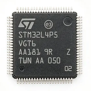
STM32F103VGT7TR - 72MHz Cortex-M3 MCU 1MB Flash 100-LQFP | ST (Tape & Reel)
MPN: STM32F103VGT7TR ✓ AktifSTM32F103VGT7TR Ringkasan
A microcontroller (MCU) is a single-chip computer that integrates a CPU core, memory and programmable I/O peripherals onto one die. Within the broader IC taxonomy, an MCU belongs to the microprocessor IC family, which sits above microcontrollers but below microprocessors in computational capability. The Cortex-M3 core inside this STM32 belongs to ARM's Cortex-M profile, designed for deterministic real-time embedded workloads; the Cortex-M3 line is one rung below Cortex-M4 in DSP capability and one rung above Cortex-M0+ in raw compute throughput.
Key features of the STM32F103VGT7TR include a 72 MHz maximum CPU clock with single-cycle multiply, two 12-bit ADCs (1 µs conversion), seven general-purpose 16-bit timers plus one PWM timer for motor control, three USARTs, two UARTs, two SPIs and one I2C, an FS-USB device, a CAN 2.0B interface, an SDIO interface, an FSMC for external memory, 80 GPIO lines and a -40 °C to +105 °C operating range. The XL-density die provides the largest Flash and SRAM footprint of the STM32F1 series, enabling sophisticated firmware with rich connectivity stacks.
The architecture pairs a Harvard-bus Cortex-M3 with a multi-AHB bus matrix that lets CPU, DMA and peripherals operate concurrently with deterministic bus latency. The 72 MHz core drives a 1.25 DMIPS/MHz figure (1.25 DMIPS/MHz), yielding 90 DMIPS total performance. The chip supports JTAG and SWD debug, an embedded Cortex-M3 trace macrocell (ETM), and boundary-scan for production test.
Typical uses include motor drives (BLDC, stepper), USB HID/COM bridges, industrial PLCs, CNC controllers, CNC and 3D-printer mainboards, data-acquisition modules, CAN-bus nodes, RFID readers and point-of-sale terminals. Designers favor the part for its mature firmware ecosystem (HAL, LL, StdPeriph), reference schematics and broad ST Nucleo board support.
When laying out, place the VDD/VSS/VBAT/VDDA pins with 100 nF decoupling within 3 mm of each power pin, plus a 1 µF bulk on VDDA; keep the HSE crystal traces short and guarded to avoid EMI on USB. Make sure the BOOT0 strap on the part is hardware-defaulted for Flash boot when designing for field upgrades. This page consolidates distributor pricing (as of 2026-10-21), pin-to-pin same-brand and cross-brand drop-in alternatives (GD32F103 series) and practical design notes not found in the manufacturer datasheet.
Alternatif penggantian untuk STM32F103VGT7TR — paket yang sama, pin-pada-pin kompatibel. Bagian paket yang berbeda memerlukan kerja ulang PCB diabaikan.
Variasi di dalam seri ini
Model-series yang sama yang kompatibel dengan penggantian STM32F103VGT7TR (sama faktor bentuk dan footprint) — berbeda di dalam Package, Flash Memory, Product Line, Product Type.
STM32F103VGT6J
✅ Drop-InKontak untuk harga
Lihat Datasheet →STM32F103VFT6
✅ Drop-InKontak untuk harga
Lihat Datasheet →STM32F103VDT7
✅ Drop-InKontak untuk harga
Lihat Datasheet →GD32F103VGT7
✅ Drop-In📋 Alternatif referensi (tidak dalam katalog)
GD32F103VFT6
✅ Drop-In📋 Alternatif referensi (tidak dalam katalog)
APM32F103VGT7
✅ Drop-In📋 Alternatif referensi (tidak dalam katalog)
STM32F103VGT7TR Rating Maksimal & Karakteristik Listrik
| Core | ARM Cortex-M3 |
| Core Architecture | 32-bit RISC, Harvard bus |
| Maximum CPU Clock | 72 MHz |
| Performance | 1.25 DMIPS/MHz (90 DMIPS) |
| Program Memory | 1 MB Flash |
| SRAM | 96 KB |
| Paket | 100-LQFP (14x14 mm) |
| Tipe Mounting | Surface Mount |
| Operating Voltage | 2.0 V to 3.6 V |
| Suhu Kerja | -40 C to +105 C |
| GPIO Count | 80 |
| ADC | 2x 12-bit, up to 16 channels, 1 MSPS |
| Timers | 7x 16-bit + 1x PWM (motor control) |
| Communication | USB FS, 2x CAN 2.0B, 3x USART, 2x UART, 3x SPI, 2x I2S, 2x I2C, SDIO, FSMC |
| Debug Interface | JTAG + SWD + ETM |
| Status RoHS | Compliant |
STM32F103VGT7TR 100-lqfp (14x14 mm) Diamant Konfigurasi Panduan
Konfigurasi pin untuk STM32F103VGT7TR (100-lqfp (14x14 mm) pakai pakai). IC digital ini termasuk GPIO, antarmuka komunikasi (UART, SPI, I2C), dan pin kuasa. Lihat datasheet produsen untuk fungsi pin alternatif dan opsi konfigurasi. Penting untuk desain sistem pengemasan dan PCB.

Tidak ada data diatribut pin yang tersedia untuk STM32F103VGT7TR.
Lihat ke: datasheet produk untuk konfigurasi pin penuh.
Aplikasi Umum
STM32F103VGT7TR cocok untuk 7 aplikasis: Brushless DC Motor Drives, USB HID / COM Bridge Devices, Industrial CAN-bus Nodes, Cobot and Industrial PLC Hubs, 3D Printer and CNC Control Boards, Medical Data-Acquisition Modules, Point-of-Sale and Vending Terminals.
Brushless DC Motor Drives
The STM32F103VGT7TR is a strong fit for BLDC and PMSM motor drives thanks to its 1 MSPS 12-bit ADC (dual ADC support for current-sense capture), one advanced PWM timer (TIM1) capable of complementary outputs with programmable dead-time, and the 72 MHz Cortex-M3 running deterministic FOC loops at 16 kHz without overload. The 1 MB Flash holds application firmware plus ST motor-control workbench libraries, and 96 KB SRAM keeps current-control buffers and observer state local for low-latency execution. The chip's CAN interface shares the PA11/PA12 bus (or PB5/PB6) with USB or other buses for CANopen integration, enabling the IC to drive 36 V/2 kW tools or e-bike hubs across multi-axis systems.
Direkomendasikan
USB HID / COM Bridge Devices
With an integrated USB 2.0 full-speed device controller and on-chip PHY, the STM32F103VGT7TR needs no external transceiver to act as a USB HID, CDC/VCP, DFU bootloader or vendor-class bridge. PA11/PA12 double as DP/DM, and 80 GPIO plus dual ADC channels let a single IC replace an external MCU+USB controller two-chip solution. Compared with smaller-density STM32F103 parts, the VGT7 has plenty of Flash for composite USB stacks (HID + CDC + vendor) plus user firmware, often making it the lowest-cost solution. Pair the design with an external EEPROM for device-serial storage and a 12 MHz HSE crystal for full USB-IF compliance.
Direkomendasikan
Industrial CAN-bus Nodes
The STM32F103VGT7TR's two bxCAN 2.0B interfaces (each with 14 filter banks and 1 Mbit/s capability) make it ideal for industrial CANopen and DeviceNet slave nodes, sensor clusters and PLC I/O modules. It withstands 105 °C ambient die temperature and integrates both an FSMC bus (for external SRAM/Flash extension) and a 1 MSPS ADC for analog backplanes, removing the need for a companion MCU. Dual bxCAN also enables CAN-bus bridge / repeater / router designs, or CAN-to-UART gateways in substation automation. Use the ST's CANopen slave stack or PEAK-System PCAN libraries; CAN tranceiver TJA1050 or TJA1051T isolates the MCU from physical bus faults.
Direkomendasikan
Cobot and Industrial PLC Hubs
The combination of 1 MB Flash (room for IEC 61131-3 runtime + safety scaffolding), 96 KB SRAM (PLC ladder logic + retentive tags), 80 GPIO, and a 12-bit ADC qualifies the STM32F103VGT7TR as a 100-MHz-class PLC main processor for cobot controllers and industrial hubs. The on-chip FSMC bus permits off-die SRAM/PSRAM extension up to 16 MB for HMI buffers and PID-loop workspaces; dual ADC supports redundant analog-input sampling; the USB and CAN interfaces connect to sensor and HMI panels. Although not AEC-Q100, the industrial -40/+105 C die temperature of the VGT7 grade suffices for cabinet-mounted controls.
Direkomendasikan
3D Printer and CNC Control Boards
The STM32F103VGT7TR's PWM timer + 1 MSPS ADC pair stepper or DC-servo control well for low-end 3D printers and CNC controllers (later revisions favor STM32F407/F411 for FPU+USB-HS). The XL-density 1 MB Flash holds Marlin/Smoothieware firmware plus user-tunable G-code optimizations; 96 KB SRAM keeps look-ahead queues and step-pulse scheduling in real time. SDIO + SPI expose SD-card interfaces for G-code files, while USB-VCP enables drop-in host wiring to PCs running Pronterface or OctoPrint. Should the application grow beyond G-code handling or need a USB-HS PHY or larger Flash, upgrade to STM32F407VGT6 in the same LQFP-100 footprint.
Direkomendasikan
Medical Data-Acquisition Modules
Although not AEC-Q100, the STM32F103VGT7TR's analog performance (dual 12-bit 1 MSPS ADC with separate VDDA), 1 MB Flash, and deterministic Cortex-M3 cores qualify it for non-invasive medical data-acquisition designs (e.g., SpO2, ECG front-ends, pulse-oximeter engines). The FSMC bus enables an external SRAM or graphics-LCD display driver. Designers add a low-side AFE like AD8232 with separate isolated power; total BOM is substantially smaller than a discrete MCU+ASIC pair. For FDA-cleared designs, engineers typically migrate to the STM32F4 family (FPU for DSP) or the STM32H7 line, but the F103VG remains common in OEM prototyping.
Direkomendasikan
Point-of-Sale and Vending Terminals
POS terminals and unattended kiosks use the STM32F103VGT7TR as a low-power Cortex-M3 main controller handling barcode readers, NFC/RFID, thermal printers, and external GPRS or Ethernet modules over UART/SPI/USB. The large Flash holds firmware for printer control, MDB (Multi-Drop Bus) peripherals, and a small embedded web-server; the on-chip CAN and FSMC expand into multi-drop beverage vending. Its 100-LQFP footprint provides abundant GPIO for keypad scanning, LCD module interfacing, and relay switching, and dual ADC channels sample battery voltage and thermistor networks for unattended-system reliability.
Direkomendasikan
Ringkasan Produk Direkomendasikan
Data referensi engineering untuk STM32F103VGT7TR — pembandingan, panduan desain, dan informasi konformitas.
Panduan Pemilihan
Pembandingan dengan Alternatif
| Parameter Umum | Produk Ini | STM32F103VGT6 | STM32F103VFT6 | GD32F103VGT7 | GD32F103VFT6 | APM32F103VGT7 | |
|---|---|---|---|---|---|---|---|
| Brand | STMicroelectronics | STMicroelectronics | STMicroelectronics | GigaDevice | GigaDevice | Geehy | |
| Package | LQFP-100 (14x14 mm) | LQFP-100 (14x14 mm) - same | LQFP-100 (14x14 mm) - same | LQFP-100 (14x14 mm) - same | LQFP-100 (14x14 mm) - same | LQFP-100 (14x14 mm) - same | LQFP-100 (14x14 mm) - same |
| Core | ARM Cortex-M3 | ARM Cortex-M3 | ARM Cortex-M3 | ARM Cortex-M3 | ARM Cortex-M3 | ARM Cortex-M3 | ARM Cortex-M3 |
| Maximum CPU Clock | 72 MHz | 72 MHz | 72 MHz | 72 MHz | 108 MHz (+50%) | 108 MHz (+50%) | 72 MHz |
| Flash Memory | 1 MB | 1 MB | 768 KB (-23%) | 384 KB (-62%) | 1 MB | 768 KB (-23%) | 1 MB |
| SRAM | 96 KB | 96 KB | 96 KB | 64 KB (-33%) | 96 KB | 96 KB | 96 KB |
| Operating Temperature | -40 C to +105 C | -40 C to +85 C (narrower) | -40 C to +85 C | -40 C to +105 C | -40 C to +85 C (industrial) | -40 C to +85 C (industrial) | -40 C to +85 C (industrial) |
| USB Full-Speed | Yes (device) | Yes (device) | Yes (device) | Yes (device) | Yes (device) | Yes (device) | Yes (device) |
| GPIO Count | 80 | 80 | 80 | 80 | 80 | 80 | 80 |
Diferensiator Kunci
- XL-density 1 MB Flash with industrial -40/+105 C die temperature (vsSTM32F103VGT6)
- 1 MB Flash + 96 KB SRAM at 72 MHz in a single LQFP-100 package (vsGD32F103VGT7)
- Mature STM32F1 ecosystem, broad support from ST's STM32CubeMX (vsAPM32F103VGT7)
Catatan Desain
Decouple each VDD/VSS pair with a 100 nF X7R capacitor within 3 mm of the pin and a bulk 4.7 µF ceramic on VDDA. Place a ferrite bead in series with VDD to VDDA and add a separate low-noise LDO on the ADC supply for noise-sensitive analog reads; the internal regulator of the VGT7 supplies 1.8 V to the core, but the VDDA supply must be in the 2.4-3.6 V range. Add 0 Ω or ferrite isolation on VBAT pin for RTC backup. Brownout-reset configuration in option bytes ensures clean state at undervoltage events.
Keep the HSE crystal trace matched to within 1 mm differential length with a guard ring to GND on each side; a 32.768 kHz LSE crystal may be omitted if your design does not need RTC, but if used, dedicate XTAL32_IN and XTAL32_OUT with minimal trace length and shield them from switching signals. PA11/PA12 (USB DP/DM) need 22 Ω series resistors, ESD protection within 5 mm of the connector, and a parasitic of <4 pF total - layout these traces at 90 Ω differential impedance and keep them away from clock and motor-driver lines. The 100-LQFP's central pad must be soldered to a copper land pour connected to GND for thermal sinking; this is critical for the full 105 °C industrial grade.
When migrating firmware to the GigaDevice GD32F103VGT7 (a common second-source drop-in), the Flash wait-state count must be re-tuned: at 108 MHz, GD32 needs 2 wait states while STM32 at 72 MHz only needs 1, otherwise you will see instruction-fetch errors. Also check that the GPIO alternate-function mapping on GD32 matches STM32 reference manual revision 'Y' or newer - older RM0008 references predate some F103V errata. Always run a Flash option-byte re-load (OB_Reload) after boot if using IAP bootloader mode, and verify the HSE bypass vs crystal oscillator mode matches the hardware configuration - mismatched boot from BOOT0 strap can silently disable JTAG/SWD and lock the part.
Although the STM32F103VGT7TR is not a power device, it can dissipate significant heat at 72 MHz with all peripherals active. The 100-LQFP θJA is about 60 °C/W on a 4-layer PCB with a 2 oz copper central pad connected to GND. In a fully populated design running a USB stack and CAN trigger, total power is around 100 mA at 3.3 V (approx 330 mW). Driving the part in a sealed industrial enclosure at 105 °C with inadequate copper will throttle the CPU; ensure a minimum copper pour of 1 square inch or attach a small clip-on heatsink for sustained thermal headroom.
Informasi Konformitas
ECOPACK2 RoHS+Pb-free package per ST datasheet. Industrial grade only; for automotive AEC-Q100, use STM32F103VG-Q1 (different ordering code). REACH SVHC251-compliant per ST product page.