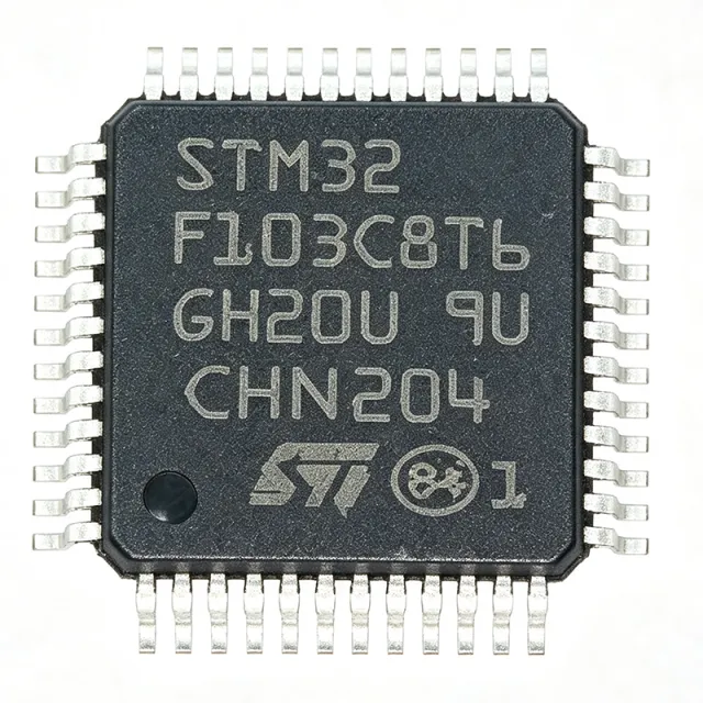
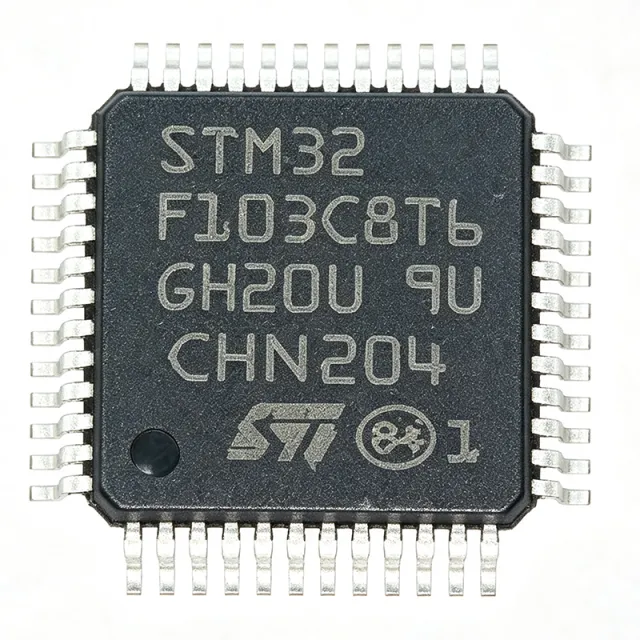
STM32F091CCU7
STM32F091CCU7 - 48MHz Cortex-M0 MCU | STMicroelectronics
STMicroelectronics STM32F091CCU7 is a 32-bit ARM Cortex-M0 microcontroller operating up to 48 MHz, with 256 KB of embedded Flash memory and 32 KB of SRAM, in a 48-pin UFQFPN package measuring 7 x 7 mm. The device combines a compact general-purpose MCU format with CAN connectivity, a 12-timer subsystem, ADC, DAC, and extensive serial peripherals for embedded control applications.
A microcontroller is a programmable semiconductor that integrates a CPU core, nonvolatile program memory, volatile data memory, and peripherals such as communications controllers, timers, analog converters, and digital I/O. Within the embedded-system hierarchy, the STM32F091 belongs to STMicroelectronics’ STM32F0 family of 32-bit ARM Cortex-M0 microcontrollers, combining low-complexity control with a broad peripheral set in a surface-mount package.
The principal features include a 48 MHz ARM Cortex-M0 RISC core, 256 KB of Flash, and 32 KB of SRAM with hardware parity-CRC capability. The integrated CAN controller supports CAN 2.0A and CAN 2.0B active specifications, including standard 11-bit and extended 29-bit identifiers, with bit rates up to 1 Mbit/s. Twelve timers support timing, PWM, motor-control, and input-capture tasks, while the ADC and DAC reduce the need for external analog components in measurement and signal-generation systems.
The STM32F091 architecture is suited to cost-conscious embedded platforms requiring deterministic peripheral access without a high-complexity processor. Its 32-bit Cortex-M0 instruction set supports efficient event handling and control loops, while integrated communication peripherals allow the device to operate as a local CAN controller. The 256 KB Flash capacity is suitable for firmware, configuration data, and application logic, while 32 KB of SRAM supports working state, stacks, buffers, and peripheral data structures.
Typical uses include industrial CAN nodes, motor and solenoid controllers, building automation equipment, sensor hubs, actuator interfaces, and compact consumer-control products. The CAN interface is particularly useful when the MCU must exchange cyclic or diagnostic data across a multi-node network. The ADC supports analog measurement, the DAC supports programmable analog output, and the timer bank enables precise timing relationships for motor-drive, lighting, and general-purpose control applications.
Board design should account for the dense 7 x 7 mm UFQFPN footprint, exposed-pad thermal requirements, and clean supply routing. Place input and output decoupling capacitors close to the relevant power pins, provide adequate high-frequency return paths beneath the device, and follow the manufacturer’s land-pattern and exposed-pad guidance. Firmware should be validated for startup sequencing, peripheral clock configuration, CAN termination, and analog-reference noise before production release.
This product page combines the manufacturer’s technical specification, package information, interface details, sourcing availability, and engineering guidance. It also organizes same-family drop-in candidates by memory and temperature options, helping designers evaluate PCB reuse while recognizing that firmware, qualification, and production validation remain necessary for each replacement decision.
見積もり
お問い合わせ