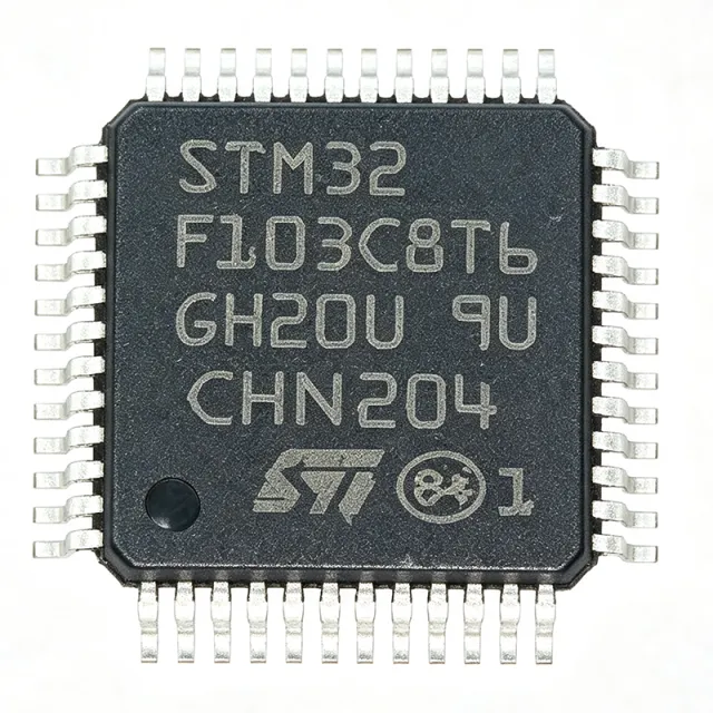
STM32F103C8T6 - 72MHz Cortex-M3 MCU、64KBフラッシュ、LQFP-48 | STMicroelectronics
部品番号: STM32F103C8T6 ✓ 生産中| 数量 | 単価 | 小計 |
|---|---|---|
| 1 | $3.1 | $3.10 |
| 10 | $2.78 | $27.80 |
| 100 | $2.45 | $245.00 |
| 500 | $2.18 | $1,090.00 |
| 1,000 | $1.92 | $1,920.00 |
| 3,000 | $1.68 | $5,040.00 |
STM32F103C8T6 概要
ARM Cortex-M3マイクロコントローラ(MCU)は、Arm Holdingsが低消費電力で決定論的なリアルタイム性能を必要とする組み込みアプリケーション向けに設計した32ビットRISCプロセッサコアです。Cortex-M3はCortex-Mファミリの下位側(Cortex-M0/M0+より上位、Cortex-M4/M7より下位)に位置し、このカテゴリのマイクロコントローラはプロセッサコアとオンチップメモリ、ペリフェラル、アナログブロックを単一のシステムオンチップに統合しています。STM32F103ファミリは特に、より広い階層(ARM Cortex-M3 -> 32ビットMCU -> STM32F1シリーズ -> STM32メインストリームファミリ -> STMicroelectronicsマイクロコントローラ -> 半導体)に属します。この階層は、ツールチェーン(Arm Cortex-M3は標準のArm Keil、IAR、GCC、STM32CubeIDEフローをサポート)と、STM32プラットフォーム全体で使用されるペリフェラルプログラミングモデルを決定するため重要です。
主な特長は、リードホワイルライト機能付き64 KBの組み込みフラッシュ、20 KBのSRAM、2.0 V~3.6 Vの電源範囲、PLL逓倍で72 MHzまで動作する8 MHz内部RC発振器、2つの12ビットADC(1 µs変換、最大16チャネル)、7つの16ビットタイマ、フルスピードUSB 2.0 Full-Speedデバイス/ホスト/OTGコントローラです。通信ペリフェラルには3つのUSART、2つのSPI(18 Mbit/s)、2つのI2Cバス(400 kHz)、1つのCAN 2.0Bインターフェース、1つのUSB Full-Speedポートが含まれます。48ピンLQFPパッケージは5 Vトレラントの37本のGPIOピンを提供します。
アーキテクチャ上、Cortex-M3コアは1 MHzあたり1.25 Dhrystone MIPSを実現し、Thumb-2命令セットをサポートし、設定可能な優先度とハードウェアスタック処理を備えたネストベクタ割り込みコントローラ(NVIC)を内蔵しています。統合電圧レギュレータとブラウンアウトリセット(BOR)により電源設計が簡素化され、タンパ検出ピン付きの4バイトバックアップレジスタはバッテリバックアップRTCモードをサポートします。
代表的なアプリケーションには、産業用制御ボード、モータドライブ(BLDC/PMSM FOCの補完)、USB HID/COMポートデバイス、CANバスノードインターフェース、そして有名な「Blue Pill」ボードなどの低コスト開発プラットフォームが含まれます。
このデバイスで設計する際は、各VDD/VDDAピンペアのできるだけ近くに100 nFセラミックデカップリングコンデンサを配置し、NRSTピン接続には10 kΩプルアップとオプションのリセットボタンを用意してください。電源投入ごとにBOOT0ピンの状態が目的のブートメモリと一致することを確認してください。
このページは、ディストリビュータ価格、ドロップイン代替品(まず同一ブランドのSTM32F103バリアント、次にクロスブランドのピン互換部品)、およびメーカーデータシートにはない実用的な設計ノートをまとめたものです。
ドロップイン代替品: STM32F103C8T6 — 同一パッケージでピン互換。PCBの作り直しが必要な異なるパッケージの部品は除外されています。
クイック比較ツール — 並列比較する代替部品を選択:
STM32F103CBT6
✓ 在庫あり
$3.2 / 個
データシートを見る →STM32F030C8T6
✓ 在庫あり
$0.98 / 個
データシートを見る →STM32F103C8T7
📋 参考代替品(カタログ未掲載)
GD32F103C8T6
📋 参考代替品(カタログ未掲載)
APM32F103C8T6
📋 参考代替品(カタログ未掲載)
STM32F103C8T6 最大定格&電気的特性
| Core Architecture | ARM Cortex-M3 (32-bit RISC) |
| 最大クロック周波数 | 72 MHz |
| Flash Memory | 64 KB |
| SRAM | 20 KB |
| Supply Voltage (VDD) | 2.0 V to 3.6 V |
| パッケージ | LQFP-48 (7x7 mm, 0.5 mm pitch) |
| GPIO Count | 37 |
| ADC | 2x 12-bit, 1 µs, up to 16 channels |
| Timers | 7x 16-bit (including 1x watchdog, 2x SysTick) |
| USART | 3 |
| SPI | 2 (18 Mbit/s) |
| I2C | 2 (400 kHz) |
| USB | 1x USB 2.0 Full-Speed device/host/OTG |
| CAN | 1x CAN 2.0B |
| 動作温度 | -40 °C to +85 °C (industrial grade) |
| RoHS ステータス | Compliant |
STM32F103C8T6 ピン構成
| ピン 1 | VBAT — Backup battery supply input |
| ピン 2 | PC13 — GPIO PC13, anti-tamper (RTC) |
| ピン 3 | PC14 — GPIO PC14 / OSC32_IN |
| ピン 4 | PC15 — GPIO PC15 / OSC32_OUT |
| ピン 5 | OSC_IN — HSE oscillator input |
| ピン 6 | OSC_OUT — HSE oscillator output |
| ピン 7 | NRST — Reset input, active-low |
| ピン 8 | VSSA — Analog ground |
| ピン 9 | VDDA — Analog supply (2.4 V - 3.6 V) |
| ピン 10 | PA0 — GPIO PA0 / WKUP / ADC_IN0 / TIM2_CH1 |
| ピン 11 | PA1 — GPIO PA1 / ADC_IN1 / TIM2_CH2 |
| ピン 12 | PA2 — GPIO PA2 / USART2_TX / ADC_IN2 |
| ピン 13 | PA3 — GPIO PA3 / USART2_RX / ADC_IN3 |
| ピン 14 | PA4 — GPIO PA4 / SPI1_NSS / ADC_IN4 |
| ピン 15 | PA5 — GPIO PA5 / SPI1_SCK / ADC_IN5 |
| ピン 16 | PA6 — GPIO PA6 / SPI1_MISO / ADC_IN6 |
| ピン 17 | PA7 — GPIO PA7 / SPI1_MOSI / ADC_IN7 |
| ピン 18 | PB0 — GPIO PB0 / ADC_IN8 / TIM3_CH3 |
| ピン 19 | PB1 — GPIO PB1 / ADC_IN9 / TIM3_CH4 |
| ピン 20 | PB2 — GPIO PB2 / BOOT1 (also PB-BOOT input) |
| ピン 21 | PB10 — GPIO PB10 / I2C2_SCL / USART3_TX |
| ピン 22 | PB11 — GPIO PB11 / I2C2_SDA / USART3_RX |
| ピン 23 | VSS_1 — Digital ground |
| ピン 24 | VDD_1 — Digital supply (2.0 V - 3.6 V) |
| ピン 25 | PB12 — GPIO PB12 / SPI2_NSS / CAN2_RX |
| ピン 26 | PB13 — GPIO PB13 / SPI2_SCK / CAN2_TX / USB_DP pull-up |
| ピン 27 | PB14 — GPIO PB14 / SPI2_MISO |
| ピン 28 | PB15 — GPIO PB15 / SPI2_MOSI |
| ピン 29 | PA8 — GPIO PA8 / USART1_CK / TIM1_CH1 |
| ピン 30 | PA9 — GPIO PA9 / USART1_TX / TIM1_CH2 |
| ピン 31 | PA10 — GPIO PA10 / USART1_RX / TIM1_CH3 |
| ピン 32 | PA11 — GPIO PA11 / CAN1_RX / USBDM (USB data minus) |
| ピン 33 | PA12 — GPIO PA12 / CAN1_TX / USBDP (USB data plus) |
| ピン 34 | PA13 — GPIO PA13 / JTMS / SWDIO |
| ピン 35 | VSS_2 — Digital ground |
| ピン 36 | VDD_2 — Digital supply (2.0 V - 3.6 V) |
| ピン 37 | PA14 — GPIO PA14 / JTCK / SWCLK |
| ピン 38 | PA15 — GPIO PA15 / JTDI |
| ピン 39 | PB3 — GPIO PB3 / JTDO / TRACESWO |
| ピン 40 | PB4 — GPIO PB4 / JNTRST |
| ピン 41 | PB5 — GPIO PB5 / I2C1_SMBAI |
| ピン 42 | PB6 — GPIO PB6 / I2C1_SCL / TIM4_CH1 |
| ピン 43 | PB7 — GPIO PB7 / I2C1_SDA / TIM4_CH2 |
| ピン 44 | BOOT0 — Boot mode select (0 = Flash, 1 = System bootloader) |
| ピン 45 | PB8 — GPIO PB8 / TIM4_CH3 |
| ピン 46 | PB9 — GPIO PB9 / TIM4_CH4 |
| ピン 47 | VSS_3 — Digital ground |
| ピン 48 | VDD_3 — Digital supply (2.0 V - 3.6 V) |
主な用途
STM32F103C8T6 の用途: 6 件s: Industrial Control Boards, USB HID / Virtual COM Port Devices, BLDC / PMSM Motor Drives, CAN-Bus Node Interface, Low-Cost Development Platforms ("Blue Pill"), IoT Sensor / Smart Home Edge Nodes.
Industrial Control Boards
The STM32F103C8T6 fits industrial control boards because its 72 MHz Cortex-M3 core and 64 KB Flash comfortably handle Modbus RTU slave firmware, PID loop control, and user-interface logic on a single chip. The dual 12-bit ADCs (1 µs, up to 16 channels) sample 4-20 mA sensor inputs at the kHz rates typical of PLC analog modules, while the three USARTs (USART1/2/3) support simultaneous RS-232/RS-485 fieldbus and a debug console. The 2.0 V to 3.6 V supply range aligns with 3.3 V industrial backplanes, and the -40 °C to +85 °C operating temperature meets most cabinet-mounted equipment specs. On-board CAN 2.0B lets a single MCU handle both a sensor bus and an external CANopen master.
おすすめ
USB HID / Virtual COM Port Devices
The STM32F103C8T6's integrated USB 2.0 Full-Speed device controller (12 Mbit/s) makes it a natural fit for USB HID-class peripherals, virtual COM-port bridges, and CDC-MSC composite devices without external PHY hardware. The 72 MHz core and 20 KB SRAM execute the standard ST USB device library (and STM32CubeMX-generated middleware) with room left for application logic, while the 64 KB Flash fits typical HID report descriptors and command parsers. Its 2.0 V to 3.6 V rail tolerance lets designers tap the USB 5 V bus through an LDO and run the MCU from a single 3.3 V supply. Designers should add ESD protection (USBLC6-2SC6) and a 1.5 kΩ pull-up on the D+ line to the USB connector.
おすすめ
BLDC / PMSM Motor Drives
The STM32F103C8T6 is widely used in sensorless or hall-sensored BLDC and PMSM motor drives for low- to mid-power applications (fans, pumps, e-bike hubs). Its 72 MHz Cortex-M3 plus advanced timers (TIM1 with complementary PWM and dead-time insertion) generate the 6-step or space-vector PWM that drives a 3-phase inverter at up to tens of kHz switching. The two ADCs trigger from timer events to sample phase currents within the PWM cycle for low-latency commutation, and the quadrature encoder interface on TIM2 supports sensored FOC firmware patterns. CAN bus readiness lets the drive communicate with a central PLC, while the 2.0-3.6 V range accepts a wide range of bus-powered motor-control supplies.
おすすめ
CAN-Bus Node Interface
The STM32F103C8T6 is a battle-tested choice for CAN 2.0B node interfaces used in automotive body-electronics, industrial CANopen, and medical device buses. The bxCAN peripheral supports standard and extended frames with hardware filter banks and a 1 Mbit/s bit rate suitable for most fieldbus deployments. With 64 KB Flash the device holds small CANopen/CANFestival stacks and application logic, while three USARTs allow a companion GPS or HMI link. Operating temperature of -40 °C to +85 °C suits non-automotive nodes; designers needing AEC-Q100 should select the STM32F103C8T7 variant. Drop a 60 Ω termination resistor only on the bus ends and add a TJA1050 or TCAN332 transceiver externally.
おすすめ
Low-Cost Development Platforms ("Blue Pill")
The STM32F103C8T6 is the headline MCU of the iconic "Blue Pill" development board that became the de-facto entry ticket to ARM Cortex-M3 firmware development. Its 72 MHz core, 64 KB Flash, SWD debug pins, USB connector, and 48-pin LQFP form factor fit on a 53 x 23 mm PCB with a USB micro-B port, a 3.3 V LDO, a reset button, and boot-mode jumpers. Students and hobbyists target it with STM32CubeIDE, PlatformIO, and the Arduino STM32 core, and any prototype firmware written on the Blue Pill ports directly to custom hardware when the same MCU is kept on the production board. The LQFP-48 footprint is also shared by several GD32 and APM32 pin-compatibles, simplifying second sourcing for educational kits.
おすすめ
IoT Sensor / Smart Home Edge Nodes
The STM32F103C8T6 handles Smart Home and IoT edge nodes that need local sensor aggregation, BLE/Wi-Fi module handshaking, and OTA bootloading without committing to a high-cost M4-class part. Three USARTs (USART1/2/3) drive an ESP-01 Wi-Fi co-processor, a GPS module, and a debug console in parallel; two SPIs (up to 18 Mbit/s) talk to a LoRa SX1278 or a small TFT display; two I2C buses serve a BME280 environmental sensor and an OLED panel. The 12-bit ADC samples analog sensors such as soil-moisture probes, and the RTC plus 4-byte backup register keep a wall-clock time across deep-sleep cycles powered by a CR2032. The 2.0-3.6 V supply range supports direct lithium-ion battery operation via an LDO or buck.
おすすめ
おすすめ製品の概要
エンジニアリング参考データ: STM32F103C8T6 — 比較、設計ガイダンス、コンプライアンス情報。
選定ガイド
代替品との比較
| パラメータ | この製品 | STM32F103CBT6 | STM32F103C8T7 | GD32F103C8T6 | APM32F103C8T6 | STM32F030C8T6 |
|---|---|---|---|---|---|---|
| Brand | STMicroelectronics | STMicroelectronics | STMicroelectronics | GigaDevice | GigaDevice | STMicroelectronics |
| Package | LQFP-48 (7x7 mm) | LQFP-48 (7x7 mm) - same | LQFP-48 (7x7 mm) - same | LQFP-48 (7x7 mm) - same | LQFP-48 (7x7 mm) - same | LQFP-48 (7x7 mm) - same |
| Core | ARM Cortex-M3 | ARM Cortex-M3 | ARM Cortex-M3 | ARM Cortex-M3 | ARM Cortex-M3 | ARM Cortex-M0 (-1 class) |
| Max Clock | 72 MHz | 72 MHz | 72 MHz | 108 MHz (+50%) | 96 MHz (+33%) | 48 MHz (-33%) |
| Flash | 64 KB | 128 KB (+100%) | 64 KB | 64 KB | 64 KB | 64 KB |
| SRAM | 20 KB | 20 KB | 20 KB | 20 KB | 20 KB | 8 KB (-60%) |
| USB | USB 2.0 Full-Speed | USB 2.0 Full-Speed | USB 2.0 Full-Speed | USB 2.0 Full-Speed | USB 2.0 Full-Speed | No USB |
| CAN | 1x CAN 2.0B | 1x CAN 2.0B | 1x CAN 2.0B | 1x CAN 2.0B | 1x CAN 2.0B | No CAN |
| Automotive Grade | No (industrial -40/+85C) | No | Yes (AEC-Q100) | No | No | No |
主な差別化要因
- 同一ファミリ内でピン互換のフラッシュ倍増ドロップイン (vs STM32F103CBT6)
- 同じシリコン/ダイでAEC-Q100車載温度グレードを提供 (vs STM32F103C8T7)
- 同じLQFP-48フットプリントで2~4倍高速なコア (vs GD32F103C8T6)
設計ノート
すべてのVDD/VDDAピンペア(ピン24、36、48 / 9)のできるだけ近くに100 nFセラミックデカップリングコンデンサを配置し、メイン3.3 Vレール上に少なくとも1つの4.7 µFバルクコンデンサを20 mm以内に配置してください。VDDAには低インピーダンス接続が必要です。メイン3.3 V電源にノイズがある場合は、VDDとVDDAの間にフェライトビーズを挿入してください。バックアップバッテリを使用しない場合はVBATをVDDに接続してください。電源投入時にBOOT0ピンを常にローに保ち、フラッシュからのデフォルトブートにしてください。
8 MHz HSE水晶のトレースは短く対称に配線し、水晶はOSC_IN/OSC_OUT(ピン5/6)から5 mm以内に配置し、負荷コンデンサ(通常20-30 pF)は水晶ケースの直近でグラウンドに接続してください。USB D+/D-(PA11/PA12)は長さを一致させ(目標差分<2 mm)、1.5 kΩプルアップはMCU側ではなくコネクタの隣のD+に配置してください。NRSTには10 kΩプルアップと、リセット押しボタンを介したGNDへの低インピーダンス経路を用意してください。
CANまたはUSBを使用する場合、IEC 61000-4-2の±8 kV気中放電および±4 kV接触放電定格を満たすため、USBLC6-2SC6やPESD1CANなどのTVSダイオードアレイをコネクタの近くに追加してください。USB D+(PA12)の内部プルアップは信頼性の高いエニュメレーションには不十分です。3.3 Vへの外部1.5 kΩ抵抗を推奨します。CANバスの終端は両端に120 Ωのみを使用し、マルチノードハーネスでのスタブ抑制にはスプリットコンデンサネットワークを使用してください。
BOOT0をフローティングのままにしないでください。電源投入時にこのピンのノイズによりMCUがシステムブートローダに間欠的にブートし、アプリケーションコードが見つからないように見えます。よくある3つの間違い:(1) VBATをVDDに接続せずフローティングのままにすると、内部ダイオードが充電されバックアップレジスタの書き込みが破損する。(2) リセット後にJTAGがデフォルトでPA13/PA14を使用するため、JTAG/SWDを無効にせずにPA13/PA14をGPIOとして使用する。(3) I2CピンでGPIO出力速度を「50 MHz」に設定するとリンギングが発生する。常に外部プルアップ付きの「2 MHz」オープンドレインを選択してください。
コンプライアンス情報
RoHS-compliant per ST product page; AEC-Q100 grade is a separate SKU (STM32F103C8T7). Halogen-free status not explicitly verified in the provided data and flagged as 'unknown'.







