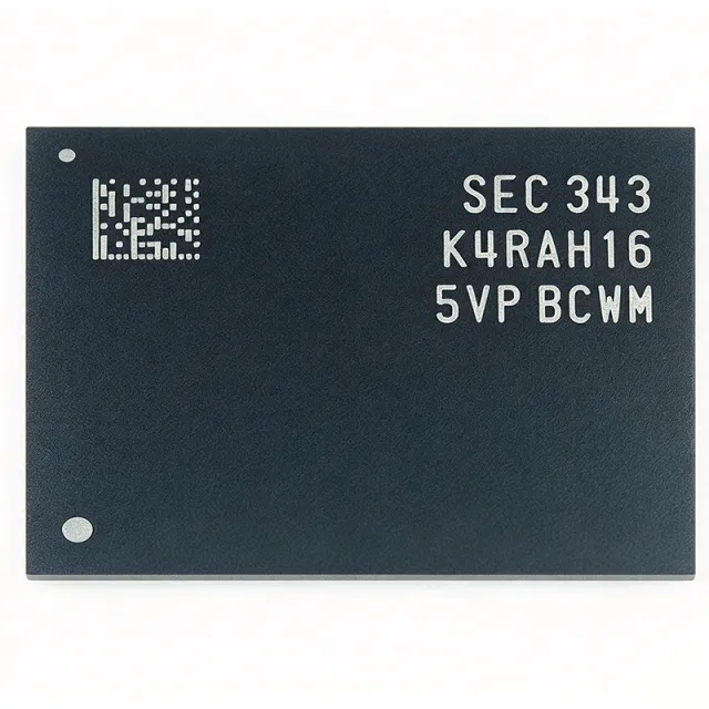
K4S281632F-TC75
K4S281632F-TC75 - 128Mb F-die SDRAM 8Mx16 TSOP-54 | Samsung
The Samsung Semiconductor K4S281632F-TC75 is a 128 Mb F-die CMOS Synchronous DRAM organized as 8M words x 16 bits, housed in a 54-pin TSOP-II (Type II) package. It operates from a single 3.3 V supply (VDD/VDDQ = 3.3 V), supports a 7.5 ns clock period (-TC75 speed grade), and is fully synchronous to the positive edge of the system clock with internal pipeline architecture that delivers high bandwidth and low latency for cost-sensitive embedded designs.
A Synchronous DRAM (SDRAM) is a type of dynamic random-access memory that adds a separate clock signal to coordinate data I/O on the rising edge, eliminating the asynchronous timing constraints of earlier FPM/EDO DRAM. SDRAM sits in the memory hierarchy between bulk storage (NAND flash, HDD) and CPU registers, and 128Mb-class parts like the K4S281632F-TC75 historically populated main memory of embedded systems, set-top boxes, networking line cards, printers, and industrial controllers throughout the 2000s before being superseded by DDR, DDR2 and Mobile SDRAM/LPDDR generations.
Key features of the K4S281632F-TC75 include dual-bank architecture (2 banks selectable via BA0), programmable CAS Latency (CL = 2 or 3), programmable Burst Length (1, 2, 4, 8, full page), Auto-Refresh and Self-Refresh modes, LVTTL-compatible I/O, and a 64 ms refresh interval distributed across 4K refresh cycles. The 16-bit data bus and on-chip burst counter simplify glue-less connection to 16/32-bit microprocessors and ASICs.
Internally, the die uses Samsung's F-die 0.13 nm-class process node and a 2-bit prefetch architecture (later generations would migrate to 4-bit prefetch with DDR). Row address is 12 bits (A0-A11) and column address is 8 bits (A0-A7) multiplexed on the same pins, with /RAS, /CAS, /WE, and /CS providing the standard SDRAM command set. The TSOP-II 54-pin form factor is the industry-standard footprint for 128 Mb x16 SDRAM, allowing board-level replacement of similar Micron, Hynix and Qimonda parts.
Typical applications for the K4S281632F-TC75 include main working memory in legacy embedded CPU boards (e.g., ARM7/ARM9 SBCs, PowerQUICC), graphics frame buffers, network switch control planes, point-of-sale terminals, automotive infotainment pre-DDR3, and other cost-optimized commercial or industrial designs where supply voltages below 2.5 V are not required. The part remains in demand today for maintenance, repair and legacy OEM replacements.
A critical design consideration is the 3.3 V supply requirement: most modern systems use 1.8 V DDR1 or 1.5 V/1.35 V DDR2/3, so the K4S281632F-TC75 cannot be retrofitted to those without a level translator. Always honor the 200 us power-on initialization sequence and the minimum 200 us wait after a CKE rise before issuing the LOAD MODE REGISTER command.
This page synthesizes distributor pricing, drop-in alternatives from Samsung and competing SDRAM vendors, and practical design notes not found in a single Samsung datasheet, providing engineers with everything needed to qualify, source, and design with the K4S281632F-TC75.
見積もり
お問い合わせ