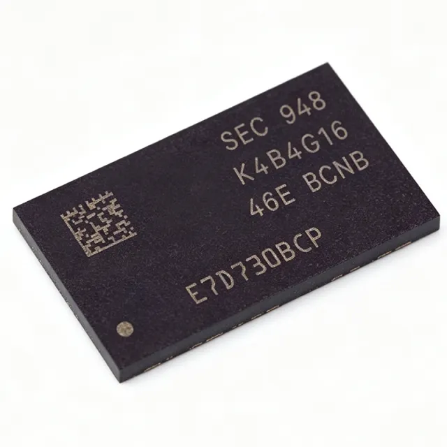
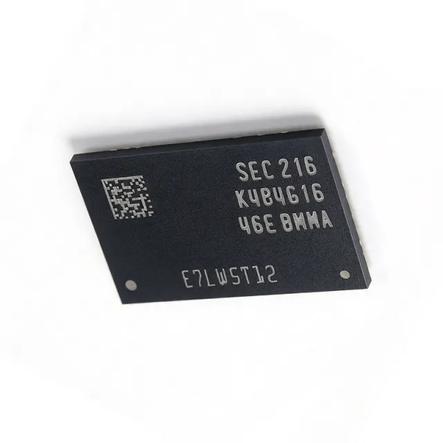
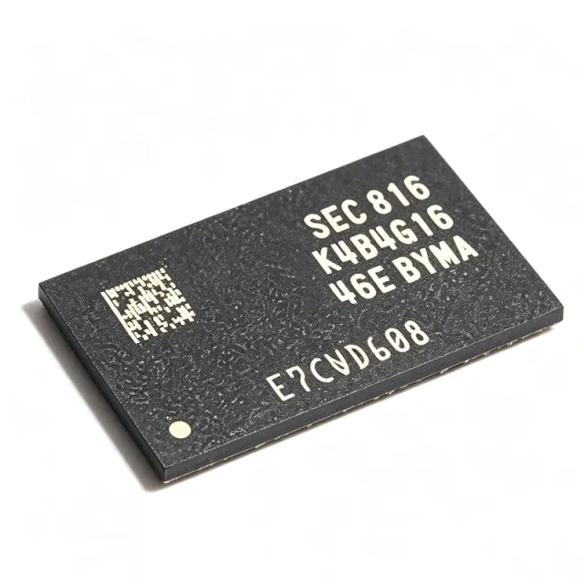
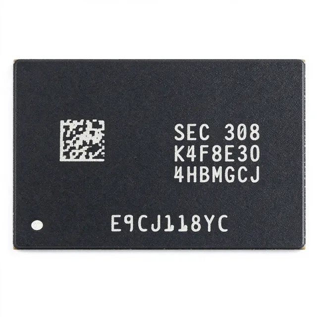
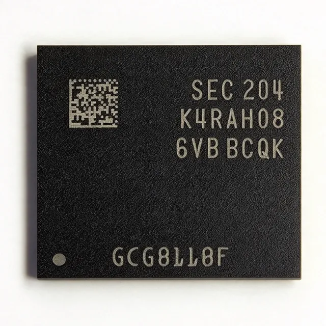
K4M56163PG-BG75
K4M56163PG-BG75 - 128Mb Mobile SDRAM, 16Mx16, 54-FBGA | Samsung
The Samsung K4M56163PG-BG75 is a 128 Mbit (4M x 16Bit x 4 Banks) Mobile Synchronous DRAM (SDRAM) organized as 16M words x 16 bits across four internal banks, housed in a 54-ball Fine-pitch Ball Grid Array (FBGA) package with a 1.8 V power supply and LVCMOS-compatible I/O. The -BG75 speed grade denotes a tCK of 7.5 ns, equivalent to a 133 MHz maximum clock frequency at full-page burst operation, while the separate /RAS, /CAS, /WE control inputs and four-bank architecture support standard SDRAM command sequences including MRS-driven CAS latency and burst length programming and EMRS-driven I/O configuration.
Mobile SDRAM is a category of synchronous DRAM that was optimized for portable, battery-powered applications in the early 2000s. Operating from a single 1.8 V rail (significantly lower than the 3.3 V required by earlier SDRAM generations), Mobile SDRAM sits in the broader taxonomy of dynamic random-access memory (DRAM) -> volatile memory -> semiconductor memory -> integrated circuit. Its four-bank internal structure allows concurrent activation of one row per bank, which hides precharge latency and improves sustained throughput versus single-bank PSRAM or SRAM alternatives in streaming workloads.
Key features of the K4M56163PG-BG75 include 4M x 16bit x 4 Banks density, 1.8 V VDD/VDDQ supply, LVCMOS-compatible inputs with multiplexed address bus, programmable CAS latency (1, 2, or 3 clocks at 133 MHz), programmable burst length (1, 2, 4, 8, or Full Page), and programmable burst type (Sequential or Interleave). Auto-refresh and self-refresh modes are supported for power-conservation duty cycles, and the device is designed for low standby current, which is essential in handheld applications. The 54-FBGA package is approximately 8 mm x 8 mm with 0.8 mm pitch, suiting compact PCB layouts in mobile devices.
In terms of architecture, the K4M56163PG-BG75 uses a four-bank SDRAM core with a 16-bit data bus, dual-bank interleaving for precharge parallelism, and a single data strobe (DQS) for source-synchronous read/write alignment. The interface follows JEDEC-compliant Mobile SDRAM signaling at 1.8 V. Compared with SRAM of identical capacity, the K4M56163PG-BG75 trades off random-access symmetry and deterministic latency for higher density per mm² and lower quiescent current in self-refresh, while still offering SDR-grade bandwidth for buffered video and frame-buffer roles.
Typical applications include mobile phone baseband working memory, PDA operating-system memory, portable media player frame buffer, handheld GPS navigation RAM, early smartphone application-processor external SDRAM, and digital camera image-processing buffers. The 54-FBGA footprint was widely adopted in mobile handsets of its era, and the 1.8 V supply simplifies PMIC integration.
When laying out a PCB for the K4M56163PG-BG75, route the 16-bit DQ group with matched trace lengths, keep the DQS strobe length-matched to within the data group, and place decoupling capacitors as close as possible to the VDD and VDDQ balls. The 0.8 mm-pitch FBGA requires via-in-pad or microvia fabrication, and an impedance-controlled layer stack is mandatory for stable read/write at 133 MHz.
This page synthesizes distributor pricing from nine sources, four-bank SDRAM drop-in alternatives, and practical layout guidance not found in the original Samsung datasheet.
見積もり
お問い合わせ