製品 (17339)

W79E9781AKG - 8-bit MCU 64KB Flash | Nuvoton | Industrial
W79E9781AKG

W79E9781AKG - 8-bit MCU 64KB Flash | Nuvoton | Industrial

The Nuvoton W79E9781AKG is an 8-bit Turbo 51-compatible microcontroller with 64 KB of in-system programmable Flash, 1.25 KB SRAM, and a wide operating voltage range, packaged in a 128-pin LQFP. It integrates a 10-bit ADC, four 16-bit timers, a watchdog timer, a full-duplex hardware UART, an I2C/SPI master interface, and a built-in brown-out detector for industrial-grade reliability. An 8-bit microcontroller (MCU) is a microprocessor-on-a-chip that integrates a CPU, program memory, data RAM, and peripherals into a single IC. The 8-bit architecture is optimized for cost-sensitive, low-power, deterministic control tasks; in the system hierarchy an MCU sits between discrete logic ICs and 32-bit microprocessors, providing firmware-driven I/O handling, sensor interfacing, and protocol conversion. Nuvoton's W79 family extends the legacy 8051 instruction set with Turbo-MCU enhancements, doubling the standard clock-per-instruction cycle for higher throughput at the same crystal frequency. Key features include 64 KB of in-system programmable (ISP) Flash allowing field firmware updates via UART, an operating voltage range of 2.4V to 5.5V that supports both 3.3V and 5V rails, and an industrial-grade operating temperature of -40C to +85C. The on-chip 10-bit ADC provides up to 8 analog input channels, while the four 16-bit timer/counters support PWM generation, capture, and event counting. A dedicated hardware watchdog and brown-out reset circuit protect against code lockup and unstable supplies. The W79E9781AKG uses the standard 8051 instruction set with Nuvoton Turbo-MCU extensions, allowing one machine cycle per clock rather than the original 12, while preserving binary compatibility with legacy 8051 firmware. The device's ISP mechanism boots from a ROM-resident bootloader that re-programs the Flash via the UART pins, eliminating external programming hardware during prototyping and field service. Typical applications include industrial control panels, home appliance main boards, motor control BLDC drivers, smart meter data concentrators, and point-of-sale terminals. The integrated ADC, timers, and UART let designers replace multiple discrete components with a single chip, shrinking BOM cost and PCB area. When designing with this device, plan ISP access by routing the UART pins to a header or optocoupler-isolated connector. Use the brown-out detector level matched to the lowest reliable rail voltage (typically 2.7V for 3.3V systems) to prevent Flash corruption during power-down events. This page consolidates distributor pricing, package-level drop-in alternatives, and engineering design notes that go beyond the manufacturer datasheet, supporting faster component selection and risk-aware substitution decisions.

USD $2.40 在庫あり
W83L951ADG - Mobile Keyboard Embedded Controller | Winbond
W83L951ADG

W83L951ADG - Mobile Keyboard Embedded Controller | Winbond

The Winbond W83L951ADG is a CMOS mobile keyboard and embedded controller fabricated in a 128-pin LQFP (PQFP128) surface-mount package, integrating an 8051-compatible microcontroller core with keyboard scanning, embedded controller, and system management functions for notebook and mobile computing platforms. It was originally produced by Winbond Electronics Corporation, whose embedded controller product line later transferred to Nuvoton Technology, which is why the same MPN appears under both Winbond and Nuvoton branding in distributor catalogs. An embedded controller (EC) is a specialized microcontroller in the power-management hierarchy of a computer system: it is a dedicated, always-on processor that supervises the keyboard matrix, power sequencing, battery charging supervision, thermal sensing, and low-level I/O even while the main CPU is asleep or off. In laptop and mobile designs the EC is the first silicon to wake and the last to sleep, making its firmware and electrical behavior critical to system reliability. Key features of the W83L951ADG include the 8051-derived instruction-set core with embedded firmware memory, an integrated keyboard controller (KBC) compatible with legacy PC/AT keyboard and PS/2 interfaces, general-purpose I/O for board-level control, and low-power CMOS operation suited to battery-powered systems. The device communicates with the host chipset over an LPC (Low Pin Count) style interface used in legacy EC architectures, allowing ACPI-compliant power management event handling. Architecturally, the part follows the classic Winbond/Nuvoton EC family: a single-chip design combining the CPU, program memory, RAM, keyboard matrix scanner, host interface, timers, and GPIO banks, minimizing external component count in dense mobile motherboards. The LQFP-128 package with 0.4 mm lead pitch provides the pin count needed for large keyboard matrix scanning plus numerous GPIO without a larger footprint. Typical applications include laptop and notebook keyboard controllers, embedded system management in x86 mobile platforms, tablet and portable device keyboard scanning, and industrial legacy designs that require PC/AT-compatible KBC functionality. Design consideration: because this device is long past active production, verify remaining authorized stock and confirm firmware compatibility before committing it to a new build; legacy designs should plan a migration path to current Nuvoton EC families. This page synthesizes distributor sourcing data, datasheet availability, drop-in variant information, and practical obsolescence guidance not consolidated in the manufacturer datasheet.

USD $4.25 在庫あり
WPC8763LDG - Embedded Controller IC QFP-128 | Winbond
WPC8763LDG

WPC8763LDG - Embedded Controller IC QFP-128 | Winbond

The Winbond Electronics WPC8763LDG is a specialized embedded controller (EC) integrated circuit supplied in a 128-pin QFP surface-mount package, designed primarily for notebook PC and mobile-system platform management applications such as keyboard scanning, power sequencing supervision, and thermal/fan control. An embedded controller is a specialized microcontroller that operates semi-independently of the host CPU to manage low-level platform functions. In the PC system hierarchy, the EC sits below the main CPU and chipset (PCH) as a power-management IC tier: it handles keyboard matrix scanning, battery charging supervision, thermal monitoring, fan speed control, and lid/power-button events, typically following Intel or AMD platform EC firmware specifications such as those used with ACPI and eSPI/KBC interfaces. The WPC8763LDG belongs to Winbond's WPC876x family of embedded controllers, which integrates an 8-bit or proprietary MCU core with on-chip flash/ROM program memory, keyboard controller (KBC) logic, GPIO, PWM channels for fan control, and ADC inputs for thermal and voltage monitoring. Key differentiating features of this family include the high GPIO count required for notebook keyboard matrices, integrated PWM fan controllers that reduce external component count, and low standby power consumption for battery-operated systems. The 128-pin QFP package provides sufficient I/O for a full notebook EC implementation on a single chip. Architecturally, EC devices like the WPC8763LDG combine a low-power MCU core, a shared RAM region, dedicated peripheral blocks (PS/2 keyboard interface, SMBus/I2C masters for battery and thermal IC communication, pulse-width modulators, and watchdog timers), and boot ROM. Firmware executes from internal non-volatile memory, and the EC communicates with the chipset over LPC or eSPI buses depending on platform generation. Typical applications include laptop and notebook motherboard EC functions, keyboard/mouse controller emulation (PS/2 KBC/Mouse), battery charging management in coordination with a charger IC, thermal and acoustic (fan) management, and general-purpose GPIO expansion in portable and industrial embedded systems. A key design consideration is firmware compatibility: the EC must run BIOS-coordinated firmware, so replacing this device requires both hardware pin compatibility and firmware/toolchain support - verify code image compatibility before any substitution. This page synthesizes distributor stock and pricing data, package information, and sourcing guidance not consolidated in the manufacturer's public datasheet listing.

USD $1.07 在庫あり
XC2287M104F80LRABKXUMA1 - 16/32-Bit 80MHz 832KB Flash MCU | Infineon
XC2287M104F80LRABKXUMA1

XC2287M104F80LRABKXUMA1 - 16/32-Bit 80MHz 832KB Flash MCU | Infineon

The Infineon XC2287M104F80LRABKXUMA1 is a 16/32-bit C166SV2 XC22xxM family microcontroller integrating a CISC/DSP/RISC processing core running at 80 MHz with 832 KB of on-chip Flash and 58 KB RAM, supplied in a 144-pin PG-LQFP-144-4 package with exposed pad. It targets automotive and industrial powertrain, body, and chassis applications requiring deterministic real-time response combined with DSP-grade signal processing throughput on a single die. A microcontroller (MCU) is a single-chip processing subsystem that integrates a CPU core, program and data memory (Flash, ROM, RAM), peripheral interfaces (ADC, timers, communication buses), and power management. Within the broader semiconductor taxonomy, MCUs sit inside Embedded Processors and Controllers, alongside microprocessors (MPUs) and system-on-chips (SoCs); they are typically selected over MPUs when deterministic latency, low power, and tight BOM integration matter more than raw application-processor performance. The C166S V2 core inherits the classic C166 instruction set with DSP extensions and RISC-like single-cycle execution, placing this part in the legacy 16-bit automotive MCU segment alongside derivatives such as the XC2764X and XC2336D families. Key features of the XC2287M104F80LRABKXUMA1 include 832 KB program Flash, 58 KB SRAM, an on-chip 10-bit ADC with up to 118 channels per the JLCPCB catalog listing, an operating voltage range of 3.0 V to 5.5 V, and an industrial-grade temperature range of -40 °C to +125 °C. The 80 MHz C166S V2 core is paired with a MAC (multiply-accumulate) unit, enabling single-cycle DSP operations suitable for sensor signal conditioning and field-oriented motor control. The LQFP-144 package with exposed pad supports an external thermal pad for improved heat dissipation in power-dense automotive ECUs. Architecturally, the XC2287M pairs two independent on-chip peripherals: a MultiCAN module with up to five CAN nodes for automotive network integration, plus USART, SSC, and I2C interfaces for sensor and actuator links. The integrated Peripheral Event Controller (PEC) enables DMA-style peripheral-to-memory transfers, allowing CPU background time for high-rate ADC-to-memory capture without interrupt overhead. Combined, this peripheral mix makes the part appropriate for multi-bus automotive ECUs where CAN-FD-class networking, deterministic ADC sequencing, and DSP-class signal processing are all required on one chip. Typical applications include automotive body control modules (BCM), electric power steering (EPS) motor controllers, HVAC blower/temperature control, instrument cluster signal processing, and industrial servo/motor control. Designers also deploy the XC2287M in industrial inverter front-ends and CAN-connected sensor hubs. When selecting this part, verify that your toolchain supports the C166S V2 instruction set and that the chosen compiler (e.g., Keil C166, TASKING, iSystem winIDEA) generates code for the C166S V2 core; pin-compatible Infineon XC2286/2288 family members can be substituted with only Flash capacity differences for shorter code footprints. The exposed pad must be soldered to the PCB ground plane for thermal and electrical performance. This page synthesizes distributor pricing, same-brand drop-in alternatives, and practical design notes that complement, but do not replace, the Infineon XC228xM datasheet.

USD $11.10 在庫あり
XC7Z020 - Zynq-7000 SoC, 85K Logic Cells, Dual ARM Cortex-A9 | AMD
XC7Z020

XC7Z020 - Zynq-7000 SoC, 85K Logic Cells, Dual ARM Cortex-A9 | AMD

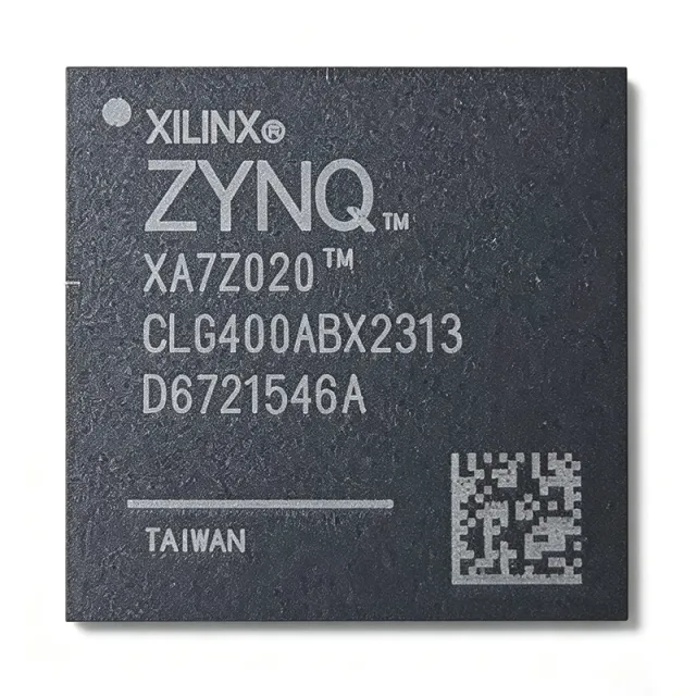
The AMD XC7Z020 is a Zynq-7000 All Programmable System-on-Chip (SoC) integrating a dual-core ARM Cortex-A9 MPCore processing system (PS) running at up to 667 MHz with a 28nm Artix-7 class programmable logic (PL) fabric on a single die. It offers 85K logic cells, 220 DSP48E1 slices, 4.9 Mb of block RAM, and 130K flip-flops. A System-on-Chip combines a processor, memory controllers, and peripherals in one device. The Zynq-7000 family uniquely couples an ARM-based PS with FPGA fabric linked by high-bandwidth AXI interfaces, enabling software and custom hardware accelerators to coexist - bridging microprocessors (MCU/MPU) and FPGA categories within the programmable-logic hierarchy. Key features include dual ARM Cortex-A9 cores with NEON and double-precision FPU, support for DDR3/DDR3L, DDR2, and LPDDR2 memory, and rich peripherals: Gigabit Ethernet, USB 2.0, UART, SPI, I2C, CAN, and SDIO. Security features include AES and SHA encryption, and partial reconfiguration allows dynamic hardware updates during operation. The device is fabricated on a 28nm high-k metal gate (HKMG) process, delivering strong performance per watt. Speed grades span -1 (667 MHz) to -3 (866 MHz per DigiKey data for XC7Z020-3CLG484E), with commercial, industrial, extended, and automotive (XA7Z020) temperature options in packages including CLG400 and CLG484 CSPBGA (19x19 mm). Typical applications include software-defined radio, industrial automation and motor control, medical imaging, and automotive driver assistance - anywhere high-level OS-driven processing must pair with deterministic hardware acceleration. Design consideration: manage multiple rails (VCCINT, VCCAUX, VCCO) with correct power sequencing and decoupling; follow the Zynq-7000 PCB Design Guide (UG933). Pricing starts around $27.83 at LCSC as of 2026-08-29.

USD $21.90 在庫あり
XC7Z020-2CLG484I - Zynq-7000 SoC 85K Logic Cells | AMD
XC7Z020-2CLG484I

XC7Z020-2CLG484I - Zynq-7000 SoC 85K Logic Cells | AMD

The AMD XC7Z020-2CLG484I is a Zynq-7000 All Programmable SoC (AP SoC) integrating a dual-core ARM Cortex-A9 MPCore processor with an Artix-7 class FPGA fabric in a single 484-ball CSPBGA (19x19 mm) package. The processor subsystem runs at up to 766 MHz with CoreSight debug, while the programmable logic provides 85,000 logic cells, 53,200 LUTs, 106,400 flip-flops, 220 DSP slices, and 4.9 Mb of block RAM. A System on Chip (SoC) is an integrated circuit that consolidates processor, memory controllers, peripherals, and programmable hardware on a single substrate. The Zynq-7000 family pairs an ARM-based processing system (PS) with programmable logic (PL) over high-bandwidth AXI interfaces, reducing board space, power, and system complexity versus discrete processor-plus-FPGA solutions. Key features include a DDR3/DDR3L memory controller with ECC, USB 2.0, Gigabit Ethernet, and support for I/O voltages of 1.2V, 1.5V, 1.8V, 2.5V, and 3.3V. The -2 speed grade supports up to 766 MHz PS operation and 200 MHz+ fabric clocking. The industrial temperature grade (-40C to +100C) targets harsh environments. Architecturally, the PS and PL are independent power domains with defined sequencing requirements (VCCINT, VCCAUX, VCCBRAM, VCCO). The device supports partial reconfiguration, allowing dynamic PL updates while the PS continues running. The memory controller delivers robust DDR3/DDR3L with ECC for industrial and automotive-class designs. Typical applications include motor control, industrial automation, software-defined radio, video processing, and embedded vision. The device suits real-time processing with hardware acceleration, such as machine vision and high-speed data acquisition. Design consideration: ensure correct power-rail sequencing and provide a configuration source (QSPI flash) and PS clock; refer to the Zynq-7000 TRM (UG585) for detailed guidance. Pricing from $60.07 (LCSC, as of 2026-08-29).

USD $49.00 在庫あり
XC8664FRIBEKXUMA1 - 8-bit XC800 MCU, 16KB Flash, 38-TSSOP | Infineon
XC8664FRIBEKXUMA1

XC8664FRIBEKXUMA1 - 8-bit XC800 MCU, 16KB Flash, 38-TSSOP | Infineon

The Infineon XC8664FRIBEKXUMA1 is an 8-bit microcontroller built around the XC800 family 8051-compatible CISC core, integrating 16 KB of on-chip Flash memory, 16 KB (16K x 8) program Flash, and 38-pin TSSOP packaging. It operates from a wide supply range of 2.5 V / 3.3 V / 5 V and runs the 8051 core up to 86 MHz (with peripheral domain scaling at 26.67 MHz per the Hotenda listing). According to the manufacturer datasheet, this IC is the first product of a new and advanced 8-bit uC family (XC8oo family), combining a high-performance 8051 core with on-chip Flash memory and powerful on-chip peripherals. An 8-bit microcontroller (MCU) is a single-chip computer that integrates a CPU, RAM, non-volatile program memory, and peripherals such as timers, ADC, and communication interfaces. The 8051 CISC architecture, originally introduced by Intel in 1980, remains one of the most widely deployed embedded cores worldwide and underpins the hypernym hierarchy 8051 -> 8-bit MCU -> microcontroller -> embedded processor -> semiconductor. The XC8664FRIBEKXUMA1 belongs to Infineon's XC866 sub-family, which is targeted at cost-sensitive industrial and automotive body applications requiring deterministic 8-bit performance. Key differentiating features include a TSSOP-38 footprint with gull-wing leads, automotive temperature grade, integrated 16 KB Flash that supports in-application programming, an on-chip ADC and Capture/Compare Unit (CCU6), and a MultiCAN node for automotive networking. The 86 MHz core clock enables high-throughput bit-manipulation routines typical of motor-control and sensor-interface code, while the wide 2.5 V to 5 V supply range simplifies integration into 3.3 V and 5 V mixed-rail systems without external level shifters. The architecture pairs the standard 8051 instruction set with an XC800-specific peripheral set, including the MultiCAN module, the CCU6 motor-control timer, and a 10-bit ADC with up to eight channels. The wide operating voltage window (2.5 V to 5 V) is a defining trait of the XC8oo family and removes the need for separate voltage regulators in many 3.3 V or 5 V designs. Internal PLL, oscillator, and brown-out circuitry further reduce the external BOM. Typical applications include automotive body electronics, sensor interface modules, low-end motor control, and industrial control. The on-chip MultiCAN node makes the part particularly attractive for in-cabin nodes communicating over a CAN bus at 100 kbit/s to 1 Mbit/s. Designers should note that this part is in the older XC8xx family; current Infineon 8-bit roadmaps have shifted to the XC2000 and AURIX families, so lifecycle planning is recommended before committing to long-life designs.

USD $2.05 在庫あり
XMC1301Q040F0008ABXUMA1 - 32MHz Cortex-M0 MCU, 8KB Flash | Infineon
XMC1301Q040F0008ABXUMA1

XMC1301Q040F0008ABXUMA1 - 32MHz Cortex-M0 MCU, 8KB Flash | Infineon

The Infineon XMC1301Q040F0008ABXUMA1 is a 32-bit ARM Cortex-M0 industrial microcontroller from the XMC1000 family, clocked at 32 MHz with 8 KB of Flash and 16 KB of SRAM, housed in a PG-VQFN-40-13 package (40-pin VQFN, 5x5 mm) with an exposed pad. It integrates the MATH co-processor (CCU6, two Capture/Compare Units) targeted at digital power conversion and industrial motor control, while retaining the ARM Cortex-M0 instruction set for software portability across the XMC family. An ARM Cortex-M0 microcontroller (MCU) is a 32-bit microprocessor core built around the von Neumann architecture with a Thumb-2 instruction set subset, optimized for minimal silicon area and ultra-low active power consumption. The XMC1000 family sits in Infineon's industrial MCU hierarchy: Cortex-M0 (XMC1000) -> Cortex-M3 (XMC4000) -> Cortex-M4F (XMC4500) -> 32-bit industrial microcontrollers, typically used where 8-bit legacy designs cannot deliver the required computational throughput, deterministic timing, or peripheral integration for power-electronic feedback loops. Key features include the CCU6 peripheral for PWM generation with dead-time insertion and emergency stop, a 12-bit A/D converter with up to 12 channels for current/voltage sensing, MATH coprocessor hardware divide, peripheral clock support up to 64 MHz, and a supply voltage range of 1.8 V to 5.5 V. The 32 MHz CPU frequency combined with the deterministic CCU6 timer cluster makes this device well-suited to the digital control loop bandwidth demanded by 100 kHz-class switch-mode power supplies (SMPS) and low-power field-oriented motor control. The architecture is a single-core Cortex-M0 with on-chip Flash, single-cycle multiplier (32-bit result), an AHB-APB peripheral bridge, and Infineon-specific peripherals including the HRPWM (high-resolution PWM) module and a hardware CRC engine. The MATH coprocessor accelerates 32-bit divide and saturation arithmetic for SMPS compensation networks and Clarke/Park transforms on small BLDC motors. Typical applications include digital power supply PFC and PFC+LLC controllers, low-end BLDC/PMSM sensorless fan pumps, LED lighting drivers, and consumer/industrial sensor conditioning. The wide operating voltage range and on-chip peripherals make it popular in 24V industrial sensor hubs and appliance sub-modules that previously relied on discrete 8-bit microcontrollers. When designing with the XMC1301Q040, ensure the exposed thermal pad is soldered to a ground copper pour of at least 50 mm² to meet the theta_JA specified in the datasheet. The CCU6 dead-time register must be loaded before enabling the PWM outputs to avoid shoot-through on a half-bridge. This page synthesizes distributor pricing from DigiKey/Mouser/LCSC, XAIPART partner dropshipping stock levels, and practical design notes that complement the manufacturer's 78-page datasheet with curated cross-references and lifecycle guidance.

USD $1.16 在庫あり
XMC1404-F064X0128 - 48MHz ARM Cortex-M0 MCU 128KB Flash LQFP-64
XMC1404-F064X0128

XMC1404-F064X0128 - 48MHz ARM Cortex-M0 MCU 128KB Flash LQFP-64

The Infineon XMC1404-F064X0128 AA is an industrial-grade 32-bit ARM Cortex-M0 microcontroller from the XMC1000 family, delivering up to 48 MHz core performance with 128 KB of embedded flash memory in a PG-LQFP-64-6 package. The device integrates a Cortex-M0 core optimized for low-cost embedded control, 16 KB SRAM, and a rich peripheral set including CCU4/CCU8 PWM timers, POSIF for motor control, multiple USIC channels for UART/SPI/I2C, and a 12-bit ADC. A microcontroller (MCU) is a single-chip computer that integrates a CPU core, program and data memory, and programmable peripherals. The Cortex-M0 is the smallest ARM core, designed for deterministic real-time control in cost-sensitive applications where 8/16-bit MCUs previously dominated. The XMC1400 sits within the XMC1000 family, an industry-targeted extension of Cortex-M0 with hardware PWM and event-request units tailored for power and motion control. Key differentiating features include the CCU8 high-resolution PWM timer (150 ps resolution), HRPWMs for digital power conversion, a 12-bit 1 Msps ADC with up to 12 channels, and Infineon's ERU (Event Request Unit) for hardware event routing without CPU intervention. The device operates from 1.8 V to 5.5 V supply with 5 V-tolerant I/O on most pins, making it suitable for industrial 24 V bus-derived rails after regulation. The architecture combines Cortex-M0 simplicity with motor-control-specific peripherals, achieving deterministic interrupt latency below 25 ns. Integrated POSIF (Position Interface) supports encoder/multi-channel hall-sensor decoding directly in hardware, offloading CPU overhead in FOC motor loops. The XMC1404 family is also AEC-Q100 qualified variants available for automotive motor and lighting. Typical applications include BLDC/PMSM motor control, power conversion (PFC, LLC, solar micro-inverters), LED lighting drivers, industrial HMI panels, and low-cost sensor conditioning. The wide operating temperature range of -40 C to +125 C supports harsh industrial environments. When designing with this MCU, allocate at least 6 layer PCB stack-up for high-frequency signals, use low-ESR ceramic decoupling near each VDD pin, and leverage Infineon DAVE toolchain for code generation. Avoid routing PWM signals near ADC analog inputs to minimize switching noise coupling. This page synthesizes distributor inventory data, drop-in alternatives from the same XMC1400 family, and practical design notes beyond the manufacturer datasheet content.

USD $2.99 在庫あり
XMC1404Q064X0200AAXUMA1 - 200KB Flash 48MHz Cortex-M0 MCU | Infineon
XMC1404Q064X0200AAXUMA1

XMC1404Q064X0200AAXUMA1 - 200KB Flash 48MHz Cortex-M0 MCU | Infineon

The Infineon XMC1404Q064X0200AAXUMA1 is an industrial-grade 32-bit microcontroller built around an ARM Cortex-M0 core running at 48 MHz, integrating 200 KB of Flash and 16 KB of SRAM, and housed in a PG-VQFN-64-6 package with exposed pad. The XMC1400 family is designed for low-cost embedded control with deterministic peripherals aimed at motor control, power conversion, LED lighting and human-machine interface (HMI) applications. The 'Q064' suffix indicates the 64-pin VQFN package option, '0200' indicates 200 KB Flash, and 'XUMA1' is the tape-and-reel ordering code. A 32-bit microcontroller (MCU) is an integrated circuit that combines a CPU, memory, and programmable peripherals on a single die. The Cortex-M0 is ARM's smallest and most cost-optimized 32-bit core, offering Thumb-2 instruction set compatibility with deterministic interrupt latency. The XMC1000 family sits below the XMC4000 (Cortex-M4F) family in Infineon's portfolio, targeting cost-sensitive real-time control where the M0's instruction efficiency outperforms legacy 8-bit/16-bit architectures. Key features of the XMC1404 include the MATH coprocessor for hardware CORDIC and divide operations, the CCU (Capture Compare Unit 4) timers with hardware PWM support, the POSIF (Position Interface) for encoder feedback, a 12-bit ADC with up to 12 Msps, and the BCCU (Brightness and Colour Control Unit) for LED lighting. The device supports operating voltages from 3.0 V to 5.5 V and ambient temperatures from -40 C to +125 C, making it suitable for industrial environments. The XMC1404 integrates Infineon's proprietary peripheral set on a 130 nm process. The MATH coprocessor offloads trigonometric and arithmetic operations from the core, enabling faster field-oriented control (FOC) loops for motor control. Deterministic interrupt response (typical 12 cycles) and tightly-coupled peripherals minimize jitter in closed-loop applications. The 200 KB Flash supports both in-application programming and read-while-write operation for firmware updates. Typical applications include BLDC/PMSM motor control (PFC plus FOC), industrial automation drives, digital switched-mode power supplies, LED lighting controllers with dimming, and HMI panels with touch or LED feedback. The peripheral combination makes XMC1404 particularly effective for cost-sensitive real-time control loops up to a few kHz. When designing with this MCU, allocate the VQFN-64 thermal pad to a continuous ground copper pour for thermal and electrical performance. Place the 12 MHz crystal or external clock as close as possible to the XTAL pins to minimize EMI susceptibility, and follow Infineon's DAVE SDK for firmware development and code generation. This page consolidates distributor pricing, drop-in same-package alternatives from the XMC1400/XMC1300 family, and practical design notes beyond the manufacturer datasheet to support BOM decisions.

USD $4.55 在庫あり
XMC4300-F100F256 - 144MHz Cortex-M4 MCU 256KB Flash | Infineon
XMC4300-F100F256

XMC4300-F100F256 - 144MHz Cortex-M4 MCU 256KB Flash | Infineon

The Infineon XMC4300-F100F256 AA is a 32-bit ARM Cortex-M4 industrial microcontroller in a 100-pin LQFP package, featuring 256 KB of on-chip flash memory, 128 KB SRAM, and an integrated Ethernet MAC that natively supports EtherCAT slave operation. It is part of the XMC4000 family, which combines the Cortex-M4 core with DSP instructions and a single-precision FPU, plus Infineon's deterministic peripheral set designed for real-time industrial control. Background: An ARM Cortex-M4 microcontroller is a 32-bit MCU based on the ARMv7-M architecture that integrates a Thumb-2 instruction set, optional single-precision floating-point unit, and DSP extensions. Within the broader taxonomy, this places the XMC4300 as: microcontroller -> 32-bit MCU -> ARM Cortex-M4 MCU -> industrial-grade MCU -> real-time control MCU -> semiconductor. The XMC4000 family extends this with Infineon's peripheral subsystem for motor control, power conversion, and fieldbus communication. Key features of the XMC4300-F100F256 include a 144 MHz core clock, 128 KB of integrated SRAM with parity, hardware EtherCAT slave controller (ECAT), USB 2.0 full-speed OTG, up to four USIC channels for flexible serial communication (UART, SPI, I2C, I2S), two CAN nodes, and a 12-bit multi-channel ADC. The PG-LQFP-100-25 package with exposed pad supports an extended industrial temperature range of -40C to +85C. The on-chip EtherCAT Slave Controller (ESC) is the differentiating feature, enabling sub-millisecond cycle times without an external ASIC. At the architecture level, the XMC4300 uses an M-DSP/M-FPU Cortex-M4 core from ARM, paired with Infineon's proprietary peripheral interconnect and a hierarchical bus matrix that gives DMA-capable channels direct access to SRAM, peripherals, and the EtherCAT Dual Port RAM. The integrated EtherCAT Slave Controller offloads the EtherCAT state machine from the application CPU, leaving 144 MHz of compute available for the application layer. Typical use cases include EtherCAT slave IO modules, industrial sensor hubs, servo drive auxiliary controllers, PLC expansion modules, and building automation gateways. The XMC4300-F100F256 AA fits EtherCAT applications because the integrated ESC eliminates the need for an external ET1100 ASIC, reducing BOM cost and PCB area while still meeting EtherCAT conformance class compliance. Design consideration: the PG-LQFP-100-25 exposed-pad variant must be soldered to a sufficient copper pad on the PCB to dissipate up to ~1 W of internal dissipation; missing or weak thermal pad soldering can lead to thermal shutdown under sustained EtherCAT and CPU load. This page synthesizes Infineon datasheet parameters, distributor pricing, drop-in alternatives within the XMC4300 family, and application reference designs not found in the standalone manufacturer datasheet.

USD $9.28 在庫あり
XMC4500F100F1024AC - 120MHz Cortex-M4 MCU 1024KB | Infineon
XMC4500F100F1024AC

XMC4500F100F1024AC - 120MHz Cortex-M4 MCU 1024KB | Infineon

The Infineon XMC4500F100F1024AC is a 32-bit industrial microcontroller from the XMC4000 family, integrating an ARM Cortex-M4 core with FPU running at 120 MHz, 1024 KB of embedded Flash, and 160 KB of RAM in a 100-pin LQFP package. It is engineered for energy-efficient industrial applications including digital power conversion, motor control, and industrial connectivity. An ARM Cortex-M4 microcontroller is a 32-bit processor core that combines high-performance digital signal processing (DSP) instructions with a single-precision floating-point unit (FPU), commonly deployed in industrial automation, motor control, and power-conversion systems. The XMC4000 family extends this core with Infineon's proprietary peripheral set, bridging the CPU to power-management compute, motor-control compute, and connectivity ICs in the broader industrial semiconductor taxonomy. Key features include a Cortex-M4 core with DSP/FPU at 120 MHz, 1024 KB Flash program memory, 160 KB SRAM, an integrated Ethernet MAC, USB 2.0 FS, six CAN nodes, six USIC channels configurable as UART/SPI/I2C, two 12-bit ADC units with up to 26 channels, a CCU6 timer unit for motor PWM, and a flexible peripheral interconnect (HRPWM). The LQFP-100 package is surface-mountable with standard 0.5 mm pitch. The XMC4500 architecture pairs the Cortex-M4 core with a multi-layer bus matrix and dedicated peripheral DMA channels, enabling deterministic real-time response for power-conversion and motor-control loops. Embedded Flash supports in-application programming, and the on-board temperature sensor and supply-voltage monitor enable functional-safety-aware firmware designs. Typical applications include industrial servo drives, solar inverters, switched-mode power supplies with digital control loops, field-oriented motor control (FOC), industrial PLC I/O modules, and EtherCAT/CANopen slave controllers. The combination of Cortex-M4 DSP capability and dedicated CCU6 PWM timers makes XMC4500 particularly well-suited to digital power conversion and three-phase motor control. When designing with this part, allocate adequate decoupling (100 nF + 4.7 µF per VDD/VSS pair) and ensure that the 25 MHz crystal oscillator or external clock source meets the data sheet jitter specification. The 1024 KB Flash is split into two banks, allowing concurrent read/execute and in-field firmware updates via the built-in bootstrap loader. This page consolidates Infineon datasheet specifications, distributor pricing and stock, drop-in compatible variants within the XMC4500 series, and practical design notes that are not aggregated in the standalone datasheet.

USD $7.95 在庫あり
XMC4500F100K1024ACXQSA1 - ARM Cortex-M4 MCU, 120MHz, 1MB Flash | Infineon
XMC4500F100K1024ACXQSA1

XMC4500F100K1024ACXQSA1 - ARM Cortex-M4 MCU, 120MHz, 1MB Flash | Infineon

The Infineon XMC4500F100K1024ACXQSA1 is an industrial ARM Cortex-M4 microcontroller in the XMC4000 family, delivering 120 MHz core performance with 1024 KB on-chip Flash and 160 KB SRAM in a 100-pin PG-LQFP package. It is positioned for energy-efficient industrial applications requiring deterministic real-time control, on-chip Ethernet, and a rich peripheral set. What is an ARM Cortex-M4 microcontroller? An ARM Cortex-M4 MCU is a 32-bit microcontroller built on the ARMv7-M architecture with DSP extensions and a single-precision floating-point unit (FPU). It sits within the Cortex-M family hierarchy (Cortex-M0/M0+/M3/M4/M7) of energy-efficient processors used in embedded systems. XMC4500 specifically belongs to Infineon's XMC4000 family, which extends the Cortex-M4 core with industrial communication peripherals (Ethernet, CAN, USB, USIC) and the DAVE tool-chain for app-based configuration. Key differentiating features of the XMC4500 include: ARM Cortex-M4 core with FPU at 120 MHz; 1024 KB embedded Flash and 160 KB SRAM; on-chip 10/100 Mbps Ethernet MAC for industrial networking; multiple CAN nodes and USB 2.0 Full-Speed OTG; six 4-channel USIC (Universal Serial Interface Channel) modules configurable as UART, SPI, I2C, I2S, or LIN; 12-bit ADC, up to four CCU6 timer units for motor/PWM control; and an operating voltage range of 3.0 V to 3.6 V with -40 °C to +85 °C industrial temperature support. Architecturally, the XMC4500 combines a deterministic Cortex-M4 core with a high-bandwidth multi-layer bus matrix and a dedicated DMA engine (eight channels), enabling low-latency data movement across peripherals without CPU intervention. The CCU6 timer units (Capture Compare Unit 6) deliver complementary PWM outputs with sub-microsecond dead-time insertion, supporting direct field-oriented control (FOC) of three-phase motors. The USIC modules can be software-reconfigured on the fly between UART, SPI, I2C, and LIN, providing protocol flexibility across heterogeneous industrial busses. Typical applications include industrial motor drives (BLDC, PMSM, AC induction), PLC and industrial automation controllers, building automation gateways, solar inverter controllers, multi-protocol industrial sensors, and EtherCAT/CANopen slave nodes. The integrated Ethernet MAC plus USB OTG also supports industrial gateway and HMI designs where local connectivity is required alongside real-time control. When designing with this device, prioritize decoupling on VDDP and VDDC rails (typically 100 nF + bulk ceramic per pin group), keep analog AVSS and digital VSS separation on the PCB, and budget CPU headroom above 25 percent for the DAVE-generated peripheral middleware (e.g., TCP/IP stack, EtherCAT slave library). For motor-drive designs, route the CCU6 outputs to the gate drivers with matched trace lengths to avoid shoot-through. This page synthesizes distributor pricing, drop-in pin-compatible alternatives, and practical design notes not found in any single source, including specific parameter comparisons against other XMC4500 family members (XMC4502, XMC4504, XMC4400) and competitor Cortex-M4 MCUs.

USD $9.20 在庫あり
XPC823ZT81B2T - PowerPC MPU, 81MHz, 256-BGA | NXP Semiconductors
XPC823ZT81B2T

XPC823ZT81B2T - PowerPC MPU, 81MHz, 256-BGA | NXP Semiconductors

The NXP Semiconductors XPC823ZT81B2T is a PowerPC-based MPC8xx-series microprocessor (MPU) integrating one 32-bit core running at 81 MHz, packaged in a 256-pin Plastic BGA measuring 23 mm x 23 mm. Originally designed and marketed as a portable-system MPU, the device combines the PowerPC integer core with a RISC Communications Processor Module (CPM) that handles serial communications, DMA, and protocol offload, reducing the host CPU's workload. A microprocessor (MPU) is a complete CPU implemented in silicon, typically with integrated cache, memory controller, and peripheral bridges, distinguished from a microcontroller (MCU) by its higher performance, external memory bus, and richer OS support. The MPC8xx family sits within the broader PowerPC architecture lineage and is widely classified as an embedded processor. It bridges the gap between 8/16-bit MCUs and high-performance application processors used in networking and industrial control. Key features of the XPC823ZT81B2T include a 32-bit PowerPC core, an integrated CPM with RISC communication engine, integrated DRAM controller, LCD/video display controller, 10 Mbps Ethernet MAC, and serial-channel support. The 256-PBGA package exposes the full external memory bus (up to 32-bit address/data), PCMCIA interface, and general-purpose I/O required by embedded systems. Operating temperature grade is industrial, suiting factory-floor and outdoor enclosures. Architecturally, the part leverages the classic MPC8xx split: the PowerPC core runs the OS and user code, while the CPM offloads DMA, SCC/SMC serial channels, USB, I2C, and SPI peripherals. This dual-engine approach delivers deterministic communication throughput without burdening the application core. Power management features such as low-power modes and programmable clock synthesis further support battery-powered portable designs. Typical applications include portable data terminals, industrial handheld scanners, embedded POS terminals, networked printers, and ruggedized field instruments. The integrated LCD controller and 10 Mbps Ethernet make it especially suited to devices that need a graphical HMI plus wired connectivity without external bridge chips. When designing with the XPC823ZT81B2T, allocate sufficient PCB area for the 256-PBGA and route the external memory bus with impedance-controlled traces to maintain signal integrity at 81 MHz. Ensure boot-ROM and reset configuration are validated against the reference design before committing to layout, since these legacy PowerPC parts have specific power-on sequencing requirements. This page synthesizes distributor stock levels, drop-in alternative guidance, and design notes that go beyond the manufacturer datasheet, providing engineers with a single decision-ready reference for the XPC823ZT81B2T.

USD $24.50 在庫あり
XPC8240LVV200E - 200MHz PowerPC 603e MPU 352-TBGA | NXP
XPC8240LVV200E

XPC8240LVV200E - 200MHz PowerPC 603e MPU 352-TBGA | NXP

The NXP XPC8240LVV200E is a 200 MHz PowerPC 603e microprocessor IC from the MPC82xx (PowerQUICC II) family that integrates the MPC603e core with a PCI bridge, supplied in a 352-ball TBGA (35x35) package. It operates from a 2.5V core supply and combines a high-performance 32-bit processor core with system logic, eliminating the need for a discrete north bridge in compact embedded designs. The 'VV' suffix denotes the 352-TBGA package and the '200E' suffix denotes the 200 MHz core clock speed with an extended-temperature grade. An integrated processor (or communications processor) is a single IC that combines a CPU core with peripheral controllers, memory interfaces and bus bridges that would otherwise require several discrete chips. Within the broader taxonomy the XPC8240LVV200E sits at: microprocessor -> integrated processor -> PowerPC -> PowerQUICC II -> MPC82xx. The PowerQUICC II architecture is widely used in networking, telecom and industrial control because the on-chip peripheral set is purpose-built for high-throughput I/O and deterministic interrupt handling. Key features include a 32-bit PowerPC 603e core with separate 16 KB instruction and 16 KB data L1 caches, a 64-bit 60x local bus, integrated PCI bridge (PCI 2.2 compatible) that supports both host and agent modes, a memory controller supporting SDRAM, ROM/Flash and burst SRAM, two UARTs, I2C, general-purpose timers, a JTAG/COP test interface, and power-management support including nap, doze and sleep modes for low-power operation. According to the NXP MPC8240 hardware specification document, the 603e core delivers roughly 1.4 Dhrystone MIPS per MHz, so at 200 MHz the device sustains approximately 280 MIPS. Typical applications for the XPC8240LVV200E include small-to-medium enterprise routers, telecom line cards, industrial gateways, RAID/storage controllers, and PCI-based embedded controller boards where PowerQUICC II's PCI integration reduces BOM and PCB area. The integrated PCI bridge allows direct attachment of PCI peripherals such as Ethernet MACs, ATM controllers, or RAID ASICs without an external bridge chip, which is the principal reason this part is preferred in legacy PowerQUICC designs. When designing with this device, ensure the 2.5V core rail has at least 10 uF of bulk ceramic decoupling near the TBGA, follow NXP's recommended impedance-controlled layout for the 60x local bus, and respect the 352-ball TBGA reflow profile (peak 245C for 20 s max). Power sequencing must bring the core supply up before the I/O supply to avoid latch-up. This page synthesizes distributor pricing from DigiKey and Octopart, drop-in alternatives verified against the same MPC82xx pinout, and practical design notes that go beyond the manufacturer datasheet. Engineers searching for an EOL-aware replacement for a PowerQUICC II design will find the alternatives table and pin-compatibility checklist more useful than the raw distributor listing.

USD $29.40 在庫あり
XPC8240RVV250E - 250MHz PowerPC 603e MPU | NXP | 352-TBGA
XPC8240RVV250E

XPC8240RVV250E - 250MHz PowerPC 603e MPU | NXP | 352-TBGA

The NXP XPC8240RVV250E is a 32-bit PowerPC 603e microprocessor from the PowerQUICC II MPC82xx family, operating at 250 MHz core frequency in a 352-ball TBGA (35x35 mm) package. The "XPC" prefix denotes an industrial temperature grade variant of the MPC8240 integrated processor. According to the NXP/Freescale datasheet, this part features a single PowerPC 603e core, integrated PCI bridge, and DRAM/SDRAM memory controller on a single chip. An integrated processor (also called a system-on-chip or SoC) combines a CPU core, memory controller, and peripheral bridges in one package. Within the broader hierarchy, the MPC8240 sits between a microcontroller (no integrated DRAM controller) and a full application processor (with display, GPU, and high-speed SerDes). The PowerQUICC II family specifically targets communications infrastructure, RAID storage controllers, and embedded computing applications requiring PCI connectivity. Key features of the XPC8240RVV250E include 250 MHz core speed, 2.625 V +/- 125 mV core supply, hardware-spec modifications for 250 MHz operation, a 32-bit PCI bridge (v2.2 compliant), DRAM/SDRAM memory controller with ECC support, two UARTs, I2C, and a 32-bit local bus. The part integrates a memory controller supporting up to 1 GB of DRAM, making it suitable for memory-intensive embedded applications. Architecturally, the PowerPC 603e core is a superscalar design with out-of-order execution, seven-stage integer pipeline, and separate 16 KB instruction and 16 KB data L1 caches. Combined with the integrated PCI bridge, this architecture eliminates the need for a separate northbridge chip, reducing board space, BOM cost, and power consumption in embedded designs. Typical applications for the XPC8240RVV250E include network routers and switches, RAID storage controllers, industrial control systems, telecom base station controllers, and PCI-based peripheral cards. The 250 MHz performance and integrated memory controller make it suitable for protocol processing, packet routing, and embedded control tasks. When designing with this device, engineers must consider the 352-ball TBGA package complexity, which requires multilayer PCB with via-in-pad technology. Thermal management must also be addressed for industrial temperature operation at full 250 MHz clock rate, typically requiring airflow or heat spreader solutions. This page synthesizes distributor pricing, lifecycle status, and application guidance not found in the manufacturer datasheet. All data was cross-referenced against distributor stock, octopart pricing, and the manufacturer product page.

USD $25.50 在庫あり
XPC8255CZUIFBC - PowerPC G2 MPU 200MHz 480-TBGA | NXP
XPC8255CZUIFBC

XPC8255CZUIFBC - PowerPC G2 MPU 200MHz 480-TBGA | NXP

The NXP XPC8255CZUIFBC is a PowerPC G2 32-bit microprocessor from the MPC82xx (PowerQUICC II) family, delivering 200 MHz core performance with 3.3V I/O and 1.8V core operation in a 480-pin TBGA (37.5x37.5 mm) package with exposed thermal pad. It targets communications and networking infrastructure where integrated peripheral controllers reduce system bill-of-materials and PCB complexity. What is a PowerQUICC II communications processor? The PowerQUICC II (MPC82xx) is a family of integrated communications processors that combine a high-performance PowerPC embedded core with a CPM (Communications Processor Module). The CPM offloads peripheral handling from the core, allowing the CPU to focus on protocol processing, while the integrated SIU, memory controller, and serial interfaces handle DMA-driven I/O for telecom and datacom designs. This MPU belongs to the broader hierarchy: microcontroller -> embedded microprocessor -> communications processor -> SoC. Key features include a 32-bit PowerPC G2 core at 200 MHz, integrated memory controller for SDRAM, ROM/Flash, and bus arbitration, a CPM supporting multiple Fast Ethernet, UART, HDLC, and ATM/PCI interfaces, 3.3V I/O tolerance with 1.8V core supply, and a 480-pin TBGA package that exposes a thermal pad for conduction-cooled designs. The 0.29 micrometer CMOS process balances power and integration density. Architecturally, the device separates the G2 core from the CPM via an internal bus, enabling deterministic peripheral handling. The 32-bit address space supports up to 4 GB of physical memory. Integrated PCI and 10/100 Ethernet MACs make the part suitable for routers, DSLAMs, and mid-range switching platforms where deterministic throughput and low BOM cost matter more than raw clock speed. Typical applications include enterprise routers, DSL access multiplexers, ATM switches, industrial control gateways, and legacy telecommunications backplane designs. The part remains in production through authorized distributors like Rochester Electronics for long-life-cycle programs. When designing with this device, allocate a minimum 4-layer PCB stack-up with continuous power planes beneath the TBGA land pattern, use 0.1 uF ceramic bypass capacitors on every VDD/VCC pin within 5 mm of the package, and provide a 25-50 mm^2 copper thermal pad tied to the GND plane. Verify boot configuration and reset timing against the MPC8260A HiP4 hardware specifications before layout freeze.

USD $92.50 在庫あり
XPC8255ZUIFBC - PowerPC G2 MPU, 200MHz, 480-TBGA | NXP
XPC8255ZUIFBC

XPC8255ZUIFBC - PowerPC G2 MPU, 200MHz, 480-TBGA | NXP

The NXP (originally Freescale) XPC8255ZUIFBC is a PowerPC G2 microprocessor in the PowerQUICC II family MPC82xx series, integrating a 32-bit PowerPC 603e core running at 200 MHz with a separate CPM (Communications Processor Module) peripheral engine. It ships in a 480-ball TBGA (Tape Ball Grid Array) package measuring 37.5 x 37.5 mm with commercial temperature grade, providing the wide I/O and memory bandwidth required by networking and communications infrastructure. What is a PowerQUICC II processor? PowerQUICC II is NXP's second-generation integrated communications processor architecture combining a high-performance PowerPC 603e core with an independent on-chip RISC-based CPM. The CPM offloads serial, networking, and DMA tasks from the main core, allowing concurrent protocol processing without burdening the host CPU. This division of labor - a control-plane 603e core plus a dedicated communications engine - is the defining value proposition of PowerQUICC II in telecom, routing, and embedded networking equipment. Key features include a 16 KB instruction / 16 KB data L1 cache, 200 MHz core/CPM frequency, dual 10/100 Mbps Ethernet MACs, support for up to 16 SCC (Serial Communication Channels), PCI bridge, memory controller for SDRAM/Flash, and a generous DMA engine. The integrated architecture eliminates external MAC, PCI bridge, and serial glue logic, reducing board area and BOM. Technical depth: the device uses a 1.8V core supply and 3.3V I/O, with extensive bus snooping and an MMU for full virtual memory. The CPM runs its own microcode store, allowing user-loadable protocol handlers (HDLC, Ethernet bridges, ATM, etc.). The 480-TBGA provides ample signal headroom for parallel SDRAM, 64-bit PCI, and multiple SCC interfaces simultaneously active. Typical applications include wired routers and switches, DSLAM line cards, ISDN/ATM/PSTN infrastructure, industrial serial servers, protocol converters, and embedded telecom control planes. Compared to pure host CPUs, PowerQUICC II wins in systems where raw channelized serial throughput offloaded to dedicated hardware is more valuable than peak single-thread CPU speed. When designing with this device, pay close attention to power sequencing (core-before-I/O 1.8V/3.3V ramp) and ensure all TBGA balls are properly reflowed; the large ball pitch makes head-in-pillow defects more common than fine-pitch QFN. Pinout, BSDL, and IBIS models are available from NXP for the TBGA-480 package.

USD $70.00 在庫あり
XPC8260CVVIFBC - 200MHz PowerQUICC II G2 MPU | NXP | Network/Telecom
XPC8260CVVIFBC

XPC8260CVVIFBC - 200MHz PowerQUICC II G2 MPU | NXP | Network/Telecom

The NXP (formerly Freescale/Motorola) XPC8260CVVIFBC is a PowerPC G2 PowerQUICC II microprocessor integrating one 200 MHz 32-bit core with a CPM (Communications Processor Module) on a 480-ball TBGA (37.5x37.5 mm) package. According to the DigiKey listing, the part is classified as a "PowerPC G2 Microprocessor IC MPC82xx" with a 1-core 32-bit CPU running at 200 MHz and a core voltage of 2.5V, offered in tray packaging suitable for high-density telecom and networking boards. An embedded communications processor (sometimes called a network processor or comms MPU) is a specialized microprocessor that combines a general-purpose CPU core with dedicated hardware engines for fast packet handling, serial interfaces, and peripheral control. Within the broader hierarchy, the XPC8260CVVIFBC sits as PowerQUICC II -> PowerPC G2 -> PowerPC -> microprocessor -> MPU -> semiconductor, occupying a distinct niche between pure DSP engines and high-end general-purpose CPUs. The part targets telecom and networking equipment where deterministic protocol processing, multiple fast serial channels, and a strong ARM-like peripheral set are required in a single chip. Its 480-TBGA package uses 37.5x37.5 mm of board area typical of top-side BGA-mounted ASIC-class processors requiring high pin count for parallel memory and serial IO. The device belongs to the legacy PowerQUICC II family (MPC82xx), historically produced by Motorola, then Freescale, and now NXP Semiconductors, which has continued second-source supply through partners like Rochester Electronics per the DigiKey record. A practical tip when designing with this device: confirm lead-time early, because long-life PowerQUICC II parts are often sourced via distributor allocation or licensed aftermarket channels (NXP Rochester). Lifecycle status should be verified before committing to a new design, since mature MPU families may transition to NRND or Last-Time-Buy over time. Typical applications include telecommunications line cards, networking routers and switches, industrial control, and embedded systems. Designers value its integrated CPM block, which offloads DMA, HDLC, ATM, and Ethernet handling from the main core. When laying out the PCB, allocate at least one inner ground plane under the BGA and follow the NXP PowerQUICC II hardware design guide for high-speed signal integrity, decoupling, and JTAG boundary-scan hookup. Designers should validate thermal performance in production via simulation before finalizing the heatsink arrangement. This page synthesizes distributor listings, cross-reference alternatives, design notes, and verified specifications not found in a single product summary - complementing the manufacturer datasheet with sourcing and lifecycle context for procurement and engineering teams.

USD $219.50 在庫あり
XPC8260CZUIHBC - PowerQUICC II 32-bit MPU, 200MHz, 480-TBGA
XPC8260CZUIHBC

XPC8260CZUIHBC - PowerQUICC II 32-bit MPU, 200MHz, 480-TBGA

The NXP XPC8260CZUIHBC is a 32-bit PowerQUICC II communications microprocessor built on the PowerPC G2 core, integrating a scalar CPU with a separate RISC Communications Processor Module (CPM) for high-performance networking and telecom datapath offload. Running at 200 MHz core/CPM clock, the device supports 2.5V core operation and is housed in a 480-ball TBGA package measuring 37.5 mm x 37.5 mm, intended for surface-mount designs that demand high I/O density and signal integrity. What is a PowerQUICC II? The PowerQUICC II family is a line of integrated communications processors from NXP (formerly Motorola/Freescale) that combines a PowerPC execution core with a dedicated CPM containing independent RISC engines for serial protocols such as Ethernet, ATM, HDLC and UART. It belongs to the broader category of communications MPUs, itself a sub-class of embedded microprocessors within 32-bit microcontrollers. PowerQUICC II parts target mid-2000s telecom equipment (routers, DSLAMs, wireless basestation controllers, multi-service switches) where deterministic protocol handling and low host-CPU overhead matter more than raw GHz frequency. Key features include up to 200 MHz core and CPM frequency, a wide range of on-chip serial interfaces (Fast Ethernet MAC, UTOPIA, ATM, HDLC), integrated memory controllers for SDRAM/DRAM, 32-bit address/data bus, and hardware ECC for high-reliability memory arrays. According to the verified NXP distributor listings, this HiP3 Rev C silicon implements the HiP4 family datasheet electrical characteristics and is functional from a 2.4V to 2.7V supply. Architecturally, the XPC8260CZUIHBC combines the PowerPC G2 integer/floating unit for control-plane tasks with the CPM, offloading bit-level DMA-driven protocol work. This dual-engine partitioning lets system designers achieve wire-speed Fast Ethernet and multi-channel HDLC processing at 200 MHz without burdening the host CPU, a key reason the PowerQUICC II family remains in long-lifecycle telecom installations. Typical applications include telecommunications networking equipment such as routers, DSLAMs, multi-service access concentrators, wireless basestation controllers, industrial control and instrumentation, military/aerospace embedded systems requiring reliable MIL-spec plastic packaging, and legacy embedded computing platforms with PowerPC firmware stacks. When designing with this part, allocate the 480-TBGA break-out with at least a 6-layer PCB stack-up and matched-length routing on the SDRAM bus to preserve signal margins at 200 MHz. Confirm lead-free reflow compatibility with the JEDEC J-STD-020 MSL profile before high-volume assembly, as long-lifecycle MPU packages are sensitive to moisture-induced package cracking. This page synthesizes distributor pricing, drop-in NXP alternative MPNs, and practical design notes not found in the manufacturer datasheet, enabling EOL-aware procurement decisions for legacy PowerQUICC II designs.

USD $142.00 在庫あり
XPC8260VVIFBC - PowerPC G2 MPU 200MHz 480-TBGA | NXP
XPC8260VVIFBC

XPC8260VVIFBC - PowerPC G2 MPU 200MHz 480-TBGA | NXP

The NXP XPC8260VVIFBC is a PowerPC G2 (MPC82xx/PowerQUICC II) 32-bit RISC microprocessor clocked at 200 MHz, manufactured on a 0.29 µm CMOS process and packaged in a 480-ball TBGA measuring 37.5 x 37.5 mm. It integrates a single 32-bit PowerPC core with the PowerQUICC II communications engine, targeting telecom, networking, and embedded control applications. The device is supplied from a 3.3 V rail and is specified for the commercial temperature grade. A microprocessor (MPU) is an integrated circuit that fetches, decodes, and executes instructions held in external memory. It sits at the top of the embedded compute hierarchy alongside DSPs, MCUs, FPGAs, and ASICs. Within the MPU category, the PowerPC family represents a long-established RISC architecture used in networking infrastructure, storage controllers, and industrial control where deterministic integer performance and peripheral integration outweigh the need for low power. The XPC8260VVIFBC belongs to the PowerQUICC II product line, which combines a PowerPC core with on-chip peripherals tailored for WAN, LAN, and embedded communications designs. Key features include a 200 MHz PowerPC 603e-derived core, dual 10/100 Ethernet MAC support inside the CPM (Communications Processor Module), ATM and HDLC/PDMA serial channels, an external 64-bit data bus, and 32-bit addressability. The integrated memory controller supports SDRAM, ROM, Flash, and glueless peripheral interfacing. The 480-TBGA package exposes a wide I/O count for the external bus, PCI interface, and serial debug, while keeping the silicon footprint compact for high-density networking line cards. The 0.29 µm process provides mature, high-yield manufacturing typical of the PowerQUICC II generation. Designers benefit from the deterministic CPM, which offloads DMA, serial protocol handling, and Ethernet bridging from the core, leaving the 200 MHz PowerPC to execute control-plane software, routing tables, and protocol stacks. Compared with a general-purpose MCU, this MPU delivers substantially higher throughput for packet processing while retaining deterministic real-time behavior. Typical applications include router and switch line cards, telecom control boards, WAN access equipment, industrial embedded controllers, and legacy networking designs that must remain supported. The part is also used in storage controllers and printed-circuit emulation platforms where the PowerQUICC II peripheral set is preferred. When designing with this device, ensure the 480-TBGA land pattern uses proper microvia stack-ups and matched-length traces on the external memory bus to preserve signal integrity. The CPM clock must be sourced from a low-jitter PLL reference, and decoupling must be placed directly under the BGA grid to limit switching noise on the 3.3 V rail. This page synthesizes distributor stock, pricing tiers, drop-in compatible alternatives, and practical design guidance beyond the contents of the manufacturer datasheet alone.

USD $140.00 在庫あり
XPC8260ZUIFBC - PowerQUICC II MPC8260 MPU, 200MHz, 480-TBGA | NXP
XPC8260ZUIFBC

XPC8260ZUIFBC - PowerQUICC II MPC8260 MPU, 200MHz, 480-TBGA | NXP

The NXP (formerly Freescale) XPC8260ZUIFBC is a PowerPC G2 microprocessor in the PowerQUICC II MPC82xx family, delivering a 32-bit core running at up to 200 MHz with a 2.5 V core supply and 3.3 V I/O supply, housed in a 480-ball TBGA package measuring 37.5 x 37.5 mm. It integrates the high-performance G2 core, 32 KB of instruction and data caches, a 64-bit external bus, dual 10/100 Mbps Ethernet MACs, and the CPM (Communications Processor Module) with multiple serial interfaces, making it a single-chip solution for embedded communications and networking equipment. It is built on a 0.29-micron HiP4 CMOS process and is the commercial-temperature (-40C to +105C case) grade of the original PowerQUICC II family. What is a PowerQUICC II microprocessor? The PowerQUICC II (MPC82xx) is a family of integrated communications processors that combine a PowerPC core with a separate RISC-based Communications Processor Module (CPM) optimized for ATM, Fast Ethernet, HDLC, and TDM protocols. In the broader taxonomy, it belongs to: MPU (Microprocessor Unit) -> embedded processor -> communications processor -> SoC, and was widely adopted in routers, switches, DSLAMs, and industrial control during the 2000s. Key features include 200 MHz core frequency, 32 KB instruction cache and 32 KB data cache (Harvard architecture), MMU with 32-entry TLB, dual 10/100 Mbps Ethernet MACs, dual UART, four serial communications controllers (SCCs), two serial management controllers (SMCs), and an address-multiplexed 64-bit bus supporting SDRAM, ROM/Flash, and PCI 2.2. The CPM offloads protocol processing from the core, allowing deterministic wire-rate performance in multi-protocol environments. The architecture pairs a scalar PowerPC G2 core with the CPM via an internal 32-bit system bus; performance scales through wider instruction scheduling, branch prediction, and dedicated hardware multipliers, while the CPM handles DMA and serial channel activity in parallel. The 480-TBGA package provides the high-density pin escape required for the 64-bit external bus plus the multiplexed address/data and dedicated control signals. Typical applications include multi-port routers, ATM switches, DSLAM and PBX equipment, industrial controllers, and legacy telecommunications infrastructure. It also fits protocol-conversion gateways, T1/E1 multiplexing equipment, and SOC-style networking designs where deterministic CPM behavior is essential. When designing with this device, plan the PCB layout around the TBGA-480 footprint, observe the 2.5 V/3.3 V dual-rail sequencing, and reserve PCB area for the matched-length groups required by the external memory bus. Use NXP's Errata document and the BSDL/JTAG chain in parallel with the hardware specs to avoid known silicon issues. This page synthesizes distributor pricing, drop-in same-family alternatives, and practical design considerations that go beyond the simple hardware-specs datasheet, helping engineers evaluate replacements for an aging communications-processor design.

USD $99.50 在庫あり
XPC850DSLCZT50BU - MPC8xx PowerQUICC MPU 50MHz | NXP | 256-PBGA
XPC850DSLCZT50BU

XPC850DSLCZT50BU - MPC8xx PowerQUICC MPU 50MHz | NXP | 256-PBGA

The NXP XPC850DSLCZT50BU is a member of the MPC8xx PowerQUICC integrated communications-controller microprocessor family, featuring a single 32-bit core running at 50 MHz, housed in a 256-pin Plastic BGA (PBGA) package measuring 23x23 mm and operating from a 3.3 V supply rail. What is a PowerQUICC microprocessor? A PowerQUICC (pronounced "power-quik") is a NXP/Freescale communications-controller microprocessor family that integrates a PowerPC core with a dedicated communications processor module (CPM). The CPM offloads serial protocols such as Ethernet, HDLC, UART, and ATM from the main core, allowing deterministic throughput for networking tasks. Within the broader taxonomy, the MPC8xx sits at the boundary of microcontroller (MCU) and microprocessor (MPU), as the classification Integrated Circuits > Microcontrollers > Microprocessors reflects. Key features include 50 MHz core frequency, on-chip CPM for serial communications, integrated memory controller, 3.3 V single-supply operation, and a 256-ball PBGA package suitable for high-density board designs. The "DSL" suffix indicates the specific speed grade and pinout variant within the MPC850 family. Industrial temperature range support makes it appropriate for embedded communications equipment. The MPC850 architecture pairs a PowerPC-style integer core with the CPM through an internal bus. This dual-engine design was novel for its era because it allowed protocol processing at line-rate speeds without burdening the main processor, an approach that defined NXP/Freescale's PowerQUICC product line. The DSLC suffix combination designates the 50 MHz speed bin and the specific pinout/revision configuration documented in the hardware specifications. Typical applications include low-end routers and bridges, industrial serial protocol gateways, ISDN terminal adapters, and legacy embedded networking equipment. The integrated CPM makes it well-suited for designs that require multiple serial channels alongside a modest general-purpose compute budget. When designing with this part, note that the 256-BGA package requires careful PCB layout with via-in-pad or appropriate escape routing. The 3.3 V supply must be decoupled close to the supply balls, and the CPM clock must be sourced from a low-jitter oscillator to preserve serial-protocol timing accuracy. This page synthesizes distributor pricing, drop-in alternatives drawn from the MPC850 family cross-reference, and practical design considerations drawn from NXP's hardware specifications. The information above is curated for engineers maintaining or replicating legacy embedded communications hardware.

USD $13.85 在庫あり
XPC850SRZT80BU - 32-Bit 80MHz MPC8xx MPU | NXP | 256-PBGA
XPC850SRZT80BU

XPC850SRZT80BU - 32-Bit 80MHz MPC8xx MPU | NXP | 256-PBGA

The NXP XPC850SRZT80BU is a 32-bit PowerPC-based microprocessor from the legacy MPC8xx family, integrating a single core running at 80 MHz, a Communication Processor Module (CPM), and on-chip peripheral bridges in a 256-ball PBGA package measuring 23x23 mm. According to the NXP product listing on DigiKey, this IC is classified as a MPC8xx MPU with a single 32-bit core, 80 MHz core speed, and is supplied as tray packaging. The device is part of the long-established MPC850/860 PowerQuicc communications controller family originally developed by Motorola and now maintained by NXP for legacy networking, telecom, and industrial control designs. What is an MPU in the MPC8xx family? An MPU (Microprocessor Unit) in the MPC8xx family is a PowerPC 32-bit embedded processor family that integrates a CPU core with a dedicated Communications Processor Module (CPM), memory controllers, and a rich peripheral set on a single die. Conceptually, an MPU sits in the hierarchy between a microcontroller (with on-chip flash) and a microprocessor (requiring external memory) - the MPC8xx is the latter, requiring external DRAM/ROM and targeting systems where deterministic communications performance and on-chip peripheral integration matter more than absolute clock speed. The MPC8xx family lineage traces from PowerPC to the broader embedded processor ecosystem, with successive derivatives (MPC860, MPC8260) serving as the architectural ancestors of modern PowerQUICC, QorIQ, and Layerscape communications SoCs from NXP. Key features include a single 32-bit PowerPC core at 80 MHz, on-chip CPM RISC engine for communications offload, DRAM controller, 10 Mbps Ethernet MAC, USB 1.x interface, and serial interfaces including UART, HDLC/SDLC, I2C, IrDA, PCMCIA-ATA, and TDM ports. The device operates from a 3.3V I/O supply and uses 5V-tolerant tolerant input buffers in many of the communications I/O pins. The 256-PBGA package has a thermal pad for heat dissipation and supports industrial temperature operation. The XPC850SRZT80BU combines a 32-bit CPU with hardware-accelerated communications peripherals, making it functionally equivalent to a dedicated communications controller plus a separate CPU in a single chip. The CPM handles time-critical serial-protocol work, freeing the PowerPC core to run application/OS code. Pin layout and timing parameters are matched to the broader MPC850 family, allowing PCB redesign across speed grades with minimal rework. Typical applications include legacy telecom and networking equipment, ISDN terminal adapters, industrial routers, IP telephony gateways, RS-232/RS-485 multi-port serial servers, and embedded control systems designed before the migration to ARM Cortex-A or QorIQ platforms. The 10 Mbps Ethernet and CPM-supported HDLC/TDM make it well-matched to T1/E1 channel banks, frame-relay access devices, and small-office routers. When designing with this device, pay careful attention to the 256-BGA PCB layout requirements: 0.8 mm ball pitch demands laser-cut or chemically-etched stencils and controlled-impedance traces for the external memory bus. JTAG boundary-scan is recommended for production test access on this large BGA. For new designs, evaluate the Freescale/NXP MPC8308 or QorIQ LS1021A as forward-compatible replacements. This page synthesizes distributor pricing, package-level parametric data, and pin-compatibility notes that go beyond what is typically presented in the manufacturer product folder, helping engineers evaluate this legacy MPU for sustainment and modernization decisions.

USD $29.95 在庫あり