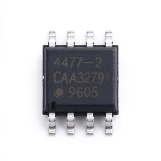
AD510KH/+ - Precision Laser-Trimmed Instrumentation Op Amp
部品番号: AD510KH/+ ✓ 生産中AD510KH/+ 概要
An operational amplifier, or op amp, is a high-gain differential amplifier that uses external feedback to control gain and bandwidth. It belongs to the linear amplifier hierarchy, which includes instrumentation amplifiers, buffer amplifiers, comparators, and voltage-feedback amplifiers. In a typical signal chain, the AD510KH/+ can amplify a sensor output, buffer a high-impedance source, or drive an analog-to-digital converter input when its input range, output swing, and stability behavior match the circuit requirements.
The AD510KH/+ is described by Analog Devices as a low-cost, laser-trimmed precision IC op amp. Laser trimming is significant because it allows the manufacturer to calibrate offset-related behavior during production, improving matching between devices and reducing the need for external offset adjustment in cost-sensitive precision circuits. The family is intended for instrumentation and buffering rather than high-speed signal processing.
The AD510KH designation identifies a specific ordering variant of the AD510 family, while the /+ suffix denotes the manufacturer's standard commercial product-ordering convention. Package, electrical limits, temperature range, and exact pin arrangement should be confirmed against the AD510 datasheet before a new PCB is released or an existing design is reworked.
Typical uses include precision bridge and sensor interfaces, instrumentation signal conditioning, analog measurement modules, and low-frequency buffer stages. In these applications, offset stability, low bias current behavior, and noise performance are more important than wideband slew rate. A practical design should verify input common-mode range at both supply rails and confirm output swing for the selected gain and load.
Keep sensitive input and feedback nodes away from switching-current paths and provide a stable reference or low-level input source through appropriate filtering. Decoupling capacitors should be placed directly across the supply pins, and the unused inputs must be tied to a defined common-mode potential rather than left floating.
This page combines the AD510KH/+ family description with sourcing guidance, same-footprint replacement analysis, application-focused engineering notes, and a parameter comparison covering alternatives that use the same 8-lead SOIC footprint. These resources help engineers evaluate the amplifier before requesting a quote or committing it to a prototype.
ドロップイン代替品: AD510KH/+ — 同一パッケージでピン互換。PCBの作り直しが必要な異なるパッケージの部品は除外されています。
このシリーズのバリエーション
同一シリーズでドロップイン互換のモデル: AD510KH/+ (同一形状・フットプリント) — 相違点: Mounting Type, Product Type.
AD510SH
✅ ドロップイン ⚠️ 仕様未検証価格はお問い合わせください
データシートを見る →AD510JH/+
✅ ドロップイン ⚠️ 仕様未検証📋 参考代替品(カタログ未掲載)
AD510AHZ
✅ ドロップイン ⚠️ 仕様未検証📋 参考代替品(カタログ未掲載)
AD510KH/+ 最大定格&電気的特性
| Product Type | Precision operational amplifier |
| Amplifier Category | Instrumentation, buffer amplifier |
| Trim Method | Laser trimmed |
| Cost Position | Low cost |
| Integrated Circuit Voltage Class | 15 V |
| パッケージ | 8-lead SOIC |
| 実装タイプ | Surface mount |
AD510KH/+ ピン構成
| ピン 1 | NC — Not connected (per datasheet) |
| ピン 2 | -IN — Inverting input |
| ピン 3 | +IN — Non-inverting input |
| ピン 4 | V- — Negative supply or ground connection |
| ピン 5 | NC — Not connected (per datasheet) |
| ピン 6 | OUT — Analog output |
| ピン 7 | V+ — Positive supply connection |
| ピン 8 | NC — Not connected (per datasheet) |
主な用途
AD510KH/+ の用途: 6 件s: Precision Sensor Signal Conditioning, Instrumentation Buffer Stage, Industrial Process Measurement, Low-Level Analog Measurement, Analog Sensor Interface, Audio and Communication Buffering.
Precision Sensor Signal Conditioning
The AD510KH/+ suits low-level sensor interfaces where a trimmed precision amplifier must operate close to the signal source. Its laser-trimmed AD510 family construction targets repeatable DC behavior, making it useful for conditioning resistive-bridge, resistance, or temperature-sensor outputs before conversion by an ADC. Place the amplifier close to the sensor to minimize parasitic capacitance and leakage on high-impedance nodes, then verify input bias current against the smallest signal of interest. The critical trade-off is that precision DC performance does not imply high bandwidth, so the operating gain must remain within the stability and noise limits shown in the manufacturer datasheet.
おすすめ
Instrumentation Buffer Stage
The AD510KH/+ can provide the impedance isolation needed between a high-impedance sensor and a following measurement or conversion stage. Because the AD510 family is laser trimmed for precision, the amplifier is appropriate when offset behavior matters more than wideband performance. Use the amplifier in a unity-gain follower when a high input impedance is the primary requirement, and keep the feedback connection extremely short to avoid added phase shift. Confirm output settling and capacitive-load behavior in the AD510 datasheet, particularly when the source includes long cables or sensor cables.
おすすめ
Industrial Process Measurement
Industrial process-control boards can use the AD510KH/+ to amplify the millivolt-level output of a bridge or transducer before it reaches an ADC or comparator. The trimmed AD510 family is attractive where repeated calibration and predictable DC offset are important in a measurement path. Place the amplifier and its input network close to the field interface, isolate high-current switching paths from the input, and include filtering only after determining the required measurement bandwidth. Validate the common-mode range at the actual sensor excitation level because the usable signal range, rather than the package rating alone, determines whether the amplifier remains accurate.
おすすめ
Low-Level Analog Measurement
The AD510KH/+ is appropriate for laboratory-style analog measurement circuits that amplify a low-level DC signal and preserve its relationship to a known reference. Laser trimming supports repeatable behavior between channels, which is useful in multi-channel measurement systems. Use a precision reference with a low-noise supply and verify that the amplifier input remains within its common-mode range at both power-up and overload conditions. Because the AD510 family prioritizes precision rather than high speed, avoid using it where the signal contains significant high-frequency content unless the closed-loop response is verified.
おすすめ
Analog Sensor Interface
A resistive or capacitive sensor can be followed by the AD510KH/+ when the interface requires gain rather than only isolation. The amplifier's laser-trimmed precision supports consistent DC operation across a bank of identical sensor channels. Design the feedback network around the required gain, keep the sensor node physically compact, and account for input bias current when the source impedance is high. Where the sensor output can exceed the amplifier's input range during fault conditions, add input clamping or protection rather than relying on the op amp's absolute maximum ratings.
おすすめ
Audio and Communication Buffering
The AD510KH/+ can buffer a low-frequency audio or communication signal when the design needs impedance isolation rather than headphone-drive capability. Its precision-trimmed character helps preserve small signals, but the application must remain inside the amplifier's bandwidth, slew-rate, output-swing, and output-current ratings. Place a small isolation resistor at the output when driving a cable or capacitive input, and test the complete load because stability behavior can differ from a resistive bench load. For wideband audio, microphone preamplification, or direct speaker drive, use an amplifier explicitly specified for those duties.
おすすめ
おすすめ製品の概要
エンジニアリング参考データ: AD510KH/+ — 比較、設計ガイダンス、コンプライアンス情報。
選定ガイド
代替品との比較
| パラメータ | この製品 | AD510 | AD510JH/+ | AD510AHZ |
|---|---|---|---|---|
| Package | 8-lead SOIC | 8-lead SOIC | 8-lead SOIC | 8-lead SOIC |
| Brand | Analog Devices | Analog Devices | Analog Devices | Analog Devices |
| Product Family | AD510 precision operational amplifier | AD510 precision operational amplifier | AD510 precision operational amplifier | AD510 precision operational amplifier |
| Amplifier Type | Single precision op amp | Single precision op amp | Single precision op amp | Single precision op amp |
| Primary Application | Instrumentation and buffer amplification | Instrumentation and buffer amplification | Instrumentation and buffer amplification | Instrumentation and buffer amplification |
主な差別化要因
- Laser-trimmed precision within a cost-conscious AD510 family (vs AD510)
- Same-footprint ordering flexibility within one manufacturer family (vs AD510JH/+)
- Instrumentation-oriented precision amplifier positioning (vs AD510AHZ)
設計ノート
Keep the non-inverting input, inverting input, and feedback components close together and away from switching-current paths. For high-impedance sensors, minimize leakage-producing contamination and guard the input node when practical. Place the supply bypass capacitors directly across pins 4 and 7, with short ground returns, and verify the complete board for unwanted antiresonant coupling rather than relying only on schematic-level values.
Do not allow either input to exceed the amplifier's specified common-mode range during startup, sensor faults, or supply transients. Tie the unused input to a defined common-mode voltage with a short, low-impedance path. When driving a capacitive load, follow the manufacturer's stability guidance and consider a small isolation resistor; adding a resistor without checking the required gain-bandwidth interaction can introduce unexpected settling behavior.
The AD510KH/+ is a precision low-level amplifier rather than a wideband driver. Filter noise at the source when possible, and keep the closed-loop bandwidth low enough to preserve the phase margin required by the datasheet. For bridge sensors, use matched input impedances and consider bias-current compensation to reduce offset generated by source resistance. Validate the finished channel with the real sensor and cable rather than with only a low-noise laboratory source.
Use a supply arrangement that keeps the amplifier within its absolute maximum and recommended operating limits, including during power-up and shutdown. The 15 V integrated-circuit class does not by itself establish the usable single-supply range. Place local decoupling at the device, keep return-current paths controlled, and verify supply noise at the amplifier pins because supply ripple can be multiplied by the closed-loop gain even when the device is described as low cost and laser trimmed.
コンプライアンス情報
The AD510KH/+ is a commercial instrumentation amplifier rather than an automotive-qualified device. Compliance statements require confirmation from the current Analog Devices product documentation and material declarations.