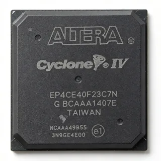
EP1K50FC484-1N - 50K-Gate ACEX-1K FPGA 250MHz 484-BGA | Intel
部品番号: EP1K50FC484-1N ✗ 生産終了| 数量 | 単価 | 小計 |
|---|---|---|
| 1 | $38.5 | $38.50 |
| 10 | $34.2 | $342.00 |
| 100 | $28.9 | $2,890.00 |
| 500 | $24.6 | $12,300.00 |
| 1,000 | $21.4 | $21,400.00 |
EP1K50FC484-1N 概要
An FPGA (Field-Programmable Gate Array) is a programmable logic device that sits between a microcontroller and a custom ASIC in the semiconductor hierarchy: ASIC → FPGA → microcontroller → general-purpose processor. FPGAs integrate configurable logic blocks (LEs), programmable interconnect, and on-chip memory so engineers can implement arbitrary digital logic, DSP pipelines, glue logic, and bus interfaces without a custom mask set. The ACEX-1K family was the first Altera family to embed dedicated array blocks (EABs) for memory or arithmetic functions, and it targets glue-logic, bus-bridging, and low-to-mid volume custom logic designs.
Key features of the EP1K50FC484-1N include 360 Logic Array Blocks (LABs), 12 Embedded Array Blocks (EABs) providing 40,960 RAM bits, multi-standard I/O support (LVTTL, LVCMOS, PCI, GTL+, SSTL-2), in-system programmability via the JTAG-compliant IEEE Std. 1149.1 interface, and 4 dedicated clock inputs with up to 6 global clock networks. The 484-FBGA package exposes 249 user I/O, giving designers ample headroom for parallel buses and memory interfaces while fitting into a surface-mount footprint.
From an architectural standpoint, each Logic Element in ACEX-1K contains a 4-input look-up table (LUT), a programmable register, and a carry chain for arithmetic. The EABs can be configured as 4,096-bit RAM or ROM blocks, allowing efficient implementation of FIFOs, lookup tables, and small algorithmic coefficient stores. The device is configured using SRAM-based configuration cells, so it loads its bitstream on every power-up from a serial PROM, JTAG, or controller.
Typical applications include communications infrastructure glue logic, peripheral-bus bridging (e.g., PCI to local bus), industrial control and instrumentation, low-volume custom DSP pre/post-processing, and test-and-measurement backplanes. The wide I/O count also suits multi-channel data-acquisition front ends and protocol-conversion cards where multiple asynchronous interfaces must be absorbed in a single device.
When designing with the EP1K50FC484-1N, plan for the 2.5 V VCCINT core rail (separate from VCCIO for I/O banks), provide a configuration source (serial configuration PROM or JTAG), and respect the FBGA-484 routing rules (escape routing on multiple layers, microvia stack if possible). The device is commercial temperature grade (0 °C to +70 °C); industrial or military temperature grades carry the "I" or "MIL" speed-grade suffix.
This page synthesizes distributor pricing, drop-in same-package alternatives, and practical design notes that complement, rather than duplicate, the manufacturer datasheet.
ドロップイン代替品: EP1K50FC484-1N — 同一パッケージでピン互換。PCBの作り直しが必要な異なるパッケージの部品は除外されています。
このシリーズのバリエーション
同一シリーズでドロップイン互換のモデル: EP1K50FC484-1N (同一形状・フットプリント) — 相違点: Speed Grade, Package, Process Technology, Configuration Method, Operating Temperature.
クイック比較ツール — 並列比較する代替部品を選択:
EP1K50FC484-1
✅ ドロップイン✓ 在庫あり
$26.4 / 個
データシートを見る →EP1K50FC484-2N
✅ ドロップイン✓ 在庫あり
$26.4 / 個
データシートを見る →EP1K50FC484-3N
✅ ドロップイン✓ 在庫あり
$19.5 / 個
データシートを見る →EP1K100FC484-1N
✅ ドロップイン✓ 在庫あり
$58.4 / 個
データシートを見る →EP1K100FC484-2N
✅ ドロップイン✓ 在庫あり
$58.4 / 個
データシートを見る →EP1K50FC484-1N 最大定格&電気的特性
| Family | ACEX-1K |
| Manufacturer | Intel (formerly Altera) |
| Logic Elements (LEs) | 2,880 |
| Typical System Gates | 50,000 |
| Maximum User I/O Pins | 249 |
| Logic Array Blocks (LABs) | 360 |
| Embedded Array Blocks (EABs) | 12 |
| Embedded Memory (Bits) | 40,960 |
| Maximum Internal Clock Frequency | 250 MHz |
| Process Technology | 0.22 µm CMOS |
| Core Supply Voltage (VCCINT) | 2.5 V |
| パッケージ | 484-ball FineLine BGA (FBGA) |
| 実装タイプ | Surface Mount |
| Speed Grade | -1 (commercial) |
| Configuration Method | SRAM, JTAG (IEEE 1149.1) |
| RoHS ステータス | Compliant (lead-free "N" suffix) |
EP1K50FC484-1N 484-ball fineline bga (fbga) ピン配置ガイド
EP1K50FC484-1N (484-ball fineline bga (fbga) パッケージ) のピン配置。 このデジタルICには、GPIO、通信インターフェース (UART、SPI、I2C)、および電源ピンが含まれています。代替ピン機能と設定オプションについては、メーカーのデータシートを参照してください。組み込みシステム設計とPCBレイアウトに不可欠です。

詳細なピン配置データはありません: EP1K50FC484-1N.
詳細は データシート をご参照ください。
主な用途
EP1K50FC484-1N の用途: 6 件s: Communications Infrastructure Glue Logic, Industrial Control & Instrumentation, PCI / Local-Bus Bridging, Test & Measurement Backplanes, Low-Volume Custom DSP Pre/Post-Processing, Legacy Peripheral & Protocol-Conversion Cards.
Communications Infrastructure Glue Logic
The EP1K50FC484-1N's 50K gates and 249 user I/O in a 484-FBGA package make it a strong fit for telecom glue-logic cards that bridge standard buses and protocol converters. Its 250 MHz internal clock and PCI-compatible I/O let it absorb protocol adaptation between legacy TDM backplanes and packet-based fabrics without external bus switches. The 12 EABs (40,960 bits of dual-port RAM) handle small cell buffers and lookup tables in place of an external SRAM, reducing BOM cost. Compared with a CPLD, the EP1K50 absorbs wider parallel buses in one device.
おすすめ
Industrial Control & Instrumentation
With 249 I/O pins and multi-standard I/O support (3.3 V LVTTL/LVCMOS, PCI, GTL+), the EP1K50FC484-1N is well-suited to industrial controllers that must interface parallel ADC/DAC banks, motor-control PWMs, and field-bus bridges in a single device. The 2.5 V core is tolerant of industrial 24 V supply rails after step-down, and the JTAG boundary-scan interface simplifies in-system programming on the production line. The device is commercial-grade (0 °C to +70 °C); for harsher industrial thermal ranges, select the I-temp variant or migrate to Cyclone IV.
おすすめ
PCI / Local-Bus Bridging
The EP1K50FC484-1N's PCI-compatible I/O pins and 50K-gate capacity let it act as a transparent bridge between a 32-bit/33 MHz PCI bus and a proprietary peripheral bus, eliminating the need for an expensive PCI bridge ASIC. Its 12 EABs (40,960 bits) can implement small FIFO buffers in dual-port mode, smoothing burst transfers across clock domains. The 484-FBGA package exposes enough user I/O to break out both 32-bit PCI and a 32-bit local bus simultaneously. Quartus IP cores provide ready-made PCI target controllers.
おすすめ
Test & Measurement Backplanes
The EP1K50FC484-1N serves well in test-and-measurement backplanes where multiple parallel data streams (LVTTL/LVCMOS) must be multiplexed, framed, and forwarded to a host processor. The 360 LABs and 12 EABs support pattern generation, error counters, and small DSP pre-processing pipelines up to 250 MHz. The 484-FBGA package enables compact PCB layouts with controlled-impedance routing for high-speed LVDS-style signals. JTAG scan chains enable board-level boundary-scan test integration on production testers.
おすすめ
Low-Volume Custom DSP Pre/Post-Processing
For low-volume designs requiring custom DSP pipelines (FIR filters, FFT pre-processing, codec rate conversion), the EP1K50FC484-1N delivers 50K gates and 12 EABs of memory at a fraction of ASIC NRE cost. The 250 MHz internal clock supports video-rate DSP at common pixel clock frequencies. Compared with a discrete DSP processor, the FPGA allows bit-width customization and parallel datapaths. Quartus DSP IP and Megafunctions simplify filter and FFT instantiation.
おすすめ
Legacy Peripheral & Protocol-Conversion Cards
The EP1K50FC484-1N is a typical solution for legacy peripheral cards that must translate between obsolete parallel protocols (VME, ISA, PC/104) and modern serial interfaces. Its wide I/O count (249 pins) accommodates several legacy buses simultaneously, and its EAB-based dual-port RAM acts as a rate-matching buffer between asynchronous domains. For long-life-cycle industrial and defense systems that must remain in production for decades, the EP1K50FC484-1N's mature tooling (Quartus II) and broad second-source availability remain an advantage.
おすすめ
おすすめ製品の概要
エンジニアリング参考データ: EP1K50FC484-1N — 比較、設計ガイダンス、コンプライアンス情報。
選定ガイド
代替品との比較
| パラメータ | この製品 | EP1K50FC484-1 | EP1K50FC484-2N | EP1K50FC484-3N | EP1K100FC484-1N | EP1K100FC484-2N |
|---|---|---|---|---|---|---|
| Brand | Intel (formerly Altera) | Intel (formerly Altera) | Intel (formerly Altera) | Intel (formerly Altera) | Intel (formerly Altera) | Intel (formerly Altera) |
| Package | 484-FBGA (FineLine BGA) | 484-FBGA (same) | 484-FBGA (same) | 484-FBGA (same) | 484-FBGA (same) | 484-FBGA (same) |
| Family | ACEX-1K | ACEX-1K | ACEX-1K | ACEX-1K | ACEX-1K | ACEX-1K |
| Typical System Gates | 50,000 | 50,000 | 50,000 | 50,000 | 100,000 (+100%) | 100,000 (+100%) |
| Logic Elements | 2,880 | 2,880 | 2,880 | 2,880 | 4,992 (+73%) | 4,992 (+73%) |
| Embedded Memory (bits) | 40,960 | 40,960 | 40,960 | 40,960 | 49,152 (+20%) | 49,152 (+20%) |
| Maximum User I/O | 249 | 249 | 249 | 249 | 333 | 333 |
| Speed Grade | -1 | -1 | -2 (faster) | -3 (fastest) | -1 | -2 (faster) |
| Lead-Free / RoHS | Yes (N) | No (no N suffix) | Yes (N) | Yes (N) | Yes (N) | Yes (N) |
主な差別化要因
- Wide 249-I/O 484-FBGA package with embedded memory (vs EP1K30FC256-3N)
- Higher logic capacity in the same 484-FBGA footprint (vs EP1K50FC484-1N vs EP1K100FC484-1N)
- Mature Quartus II toolchain with abundant legacy IP (vs Xilinx Spartan-II XC2S50)
設計ノート
The EP1K50FC484-1N requires a 2.5 V VCCINT core supply separate from VCCIO I/O bank supplies. Estimate Iccint at approximately 5-15 mA per MHz of internal toggle rate plus static EAB/IO contribution; use a low-noise LDO such as an LT3021-2.5 or TPS7A45 followed by a 22 µF + 0.1 µF ceramic decoupling network. I/O bank VCCIO must match the chosen I/O standard (3.3 V LVTTL, 2.5 V LVCMOS, 3.3 V PCI, etc.).
The 484-FBGA package requires multilayer PCB escape routing. Use microvias (laser-drilled, 6 mil pad) on at least 4 routing layers if possible, with the top layer dedicated to fan-out and inner layers for signal routing. Keep all decoupling capacitors within 100 mils of their respective supply balls and stitch GND vias on every BGA corner ball. Controlled-impedance traces (50 Ω single-ended) are mandatory for clocks and high-speed I/O.
ACEX-1K FPGAs use SRAM configuration cells, so they must reconfigure on every power-up. Provide a configuration source: a serial configuration PROM (EPC2LC20 / EPC4 / EPC8) in PS or AS mode, JTAG, or a microcontroller driving DCLK/DATA. Failure to populate the configuration source results in a non-functional board. JTAG chain integrity (TCK, TMS, TDI, TDO) must be verified with the Quartus programmer before board bring-up.
The 484-FBGA package has a θJA of approximately 15-20 °C/W (with proper PCB thermal design). For typical designs running at moderate toggle rates, junction temperature rise above ambient is under 10 °C. For high-utilization designs (>80% LE usage, high EAB bandwidth), verify thermal performance in the Quartus PowerPlay tool and add thermal vias under the BGA if needed.
コンプライアンス情報
RoHS / lead-free status inferred from the "N" suffix in the MPN per Altera / Intel naming convention. REACH, halogen-free, and conflict-mineral declarations are not present in the verified web data; consult Intel's product compliance declarations for confirmation.