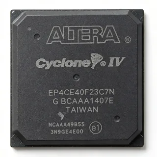
EP3C16F484C6N - Cyclone III FPGA 16K LE 484-FBGA | Intel
部品番号: EP3C16F484C6N ✓ 生産中| 数量 | 単価 | 小計 |
|---|---|---|
| 1 | $434.54 | $434.54 |
| 10 | $412.8 | $4,128.00 |
| 50 | $385.2 | $19,260.00 |
| 100 | $360.1 | $36,010.00 |
| 500 | $338.75 | $169,375.00 |
EP3C16F484C6N 概要
An FPGA (Field-Programmable Gate Array) is a programmable semiconductor containing configurable logic blocks, programmable interconnect, and programmable I/O cells that engineers can customize after manufacture to implement custom digital logic. In the programmable logic hierarchy, FPGAs sit between fixed-function ASICs (lower flexibility, lower per-unit cost at volume) and microcontrollers (sequential execution, lower parallel throughput). The Cyclone III family targets the low-power, low-cost segment of the FPGA market using TSMC's 65 nm process node.
Key features of the EP3C16F484C6N include four phase-locked loops (PLLs) for clock synthesis and skew management, 20 global clock networks, support for external memory interfaces including DDR, DDR2, and QDRII SRAM, and configuration via JTAG, passive serial, or fast passive parallel modes. The device also provides dedicated hardware blocks for PCI Express endpoint, gigabit Ethernet, and basic DSP functions.
The Cyclone III architecture uses adaptive logic modules (ALMs) instead of legacy 4-input LUTs, yielding higher effective logic density per LE. The 484-FBGA (FineLine BGA) package uses a 1.0 mm ball pitch, supporting high-density PCB designs with standard surface-mount assembly. The N suffix indicates lead-free, RoHS-compliant packaging suitable for high-volume manufacturing.
Typical applications include industrial motor control, video processing bridges, wireline telecommunications, automotive driver assistance, and embedded DSP. Designers use Quartus II or Quartus Prime design software for synthesis, place-and-route, and timing closure.
When designing with this FPGA, ensure the PCB layout uses at least four PCB layers with dedicated power and ground planes for the core (1.2 V) and I/O supplies. Decoupling capacitors must be placed as close as possible to each supply pin per Quartus power delivery guidance, and unused I/O pins should be left floating or tied to ground per the configuration handbook.
This page synthesizes distributor pricing, drop-in alternatives, and practical design notes not found in the manufacturer datasheet alone.
ドロップイン代替品: EP3C16F484C6N — 同一パッケージでピン互換。PCBの作り直しが必要な異なるパッケージの部品は除外されています。
このシリーズのバリエーション
同一シリーズでドロップイン互換のモデル: EP3C16F484C6N (同一形状・フットプリント) — 相違点: Package, Process Technology, Speed Grade, Core Voltage, Embedded Memory.
クイック比較ツール — 並列比較する代替部品を選択:
EP3C16F484C8N
✅ ドロップイン✓ 在庫あり
$29.95 / 個
データシートを見る →EP3C16F484C7N
✅ ドロップイン✓ 在庫あり
$30.1 / 個
データシートを見る →EP3C16F484I7N
✅ ドロップイン✓ 在庫あり
$36.4 / 個
データシートを見る →EP3C16U484C7N
✅ ドロップイン📋 参考代替品(カタログ未掲載)
EP3C16F484C6
✅ ドロップイン✓ 在庫あり
$42.3 / 個
データシートを見る →EP3C16F484C6N 最大定格&電気的特性
| Series | Cyclone III |
| Family | Cyclone III |
| Logic Elements (LE) | 15,408 |
| Adaptive Logic Modules (ALMs) | 963 ALMs |
| Embedded Memory | 516,096 bits (504 Kbits) |
| Embedded 18x18 Multipliers | 56 |
| User I/O Pins (max) | 346 |
| PLLs | 4 |
| Global Clock Networks | 20 |
| Core Supply Voltage | 1.15 V to 1.25 V |
| Operating Temperature (Commercial) | 0 C to 85 C |
| Speed Grade | -6 |
| パッケージ | 484-ball FineLine BGA (FBGA) |
| Ball Pitch | 1.0 mm |
| Process Technology | 65 nm TSMC |
| Configuration Modes | JTAG, Passive Serial, Fast Passive Parallel |
| 実装タイプ | Surface Mount |
| RoHS ステータス | Compliant (lead-free, N suffix) |
EP3C16F484C6N 484-ball fineline bga (fbga) ピン配置ガイド
EP3C16F484C6N (484-ball fineline bga (fbga) パッケージ) のピン配置。 このデジタルICには、GPIO、通信インターフェース (UART、SPI、I2C)、および電源ピンが含まれています。代替ピン機能と設定オプションについては、メーカーのデータシートを参照してください。組み込みシステム設計とPCBレイアウトに不可欠です。

詳細なピン配置データはありません: EP3C16F484C6N.
詳細は データシート をご参照ください。
主な用途
EP3C16F484C6N の用途: 6 件s: Industrial Motor Control, Video Processing Bridge, Wireline Telecommunications, Automotive Driver Assistance, Embedded DSP and Signal Processing, LED Display and Lighting Control.
Industrial Motor Control
The EP3C16F484C6N's 56 embedded 18x18 multipliers and 4 PLLs make it a solid match for industrial motor control loops including field-oriented control (FOC) and space-vector PWM. Its 15,408 logic elements comfortably host multi-axis PID controllers, encoder interfaces, and commutation logic, while the 346 user I/O pins connect directly to PWM outputs, Hall sensors, and resolver feedback. The 1.0 mm FBGA package integrates cleanly onto compact industrial drive PCBs. Compared with a microcontroller-only solution, the FPGA executes the control loop deterministically in hardware, achieving sub-microsecond loop times. Quartus PI: designers use the DSP Builder blockset or VHDL/Verilog cores for the FOC math; the device supports commercial 0 to 85 C ambient.
おすすめ
Video Processing Bridge
The EP3C16F484C6N's 504 Kbits of embedded memory and 56 multipliers suit video format conversion and bridging applications such as HDMI-to-LVDS, BT.656-to-USB, or camera interface aggregation. The 346 user I/O pins accept multiple parallel video streams and route them through on-chip line buffers, while LVDS support in the I/O banks enables direct connection to flat-panel displays. Designers use the Cyclone III video IP cores for scaling and color-space conversion, achieving full-HD throughput at 60 fps in this 15,408-LE device. The 484-FBGA package provides the I/O density needed for multi-channel video aggregation. Compared with an ASSP, the FPGA handles multiple formats simultaneously without external bridge chips.
おすすめ
Wireline Telecommunications
The EP3C16F484C6N serves as a framer or serializer/deserializer in wireline telecom equipment, including T1/E1 aggregation, SONET/SDH framing at lower rates, and CPRI bridges for small-cell base stations. Its 4 PLLs generate the precise clock multiples required for telecom line coding, while the 56 embedded 18x18 multipliers handle bit-error-rate calculations and scrambling. The device supports DDR and DDR2 external memory interfaces via dedicated PHY blocks, enabling large packet buffers for traffic shaping. The commercial temperature grade is sufficient for central-office environments; for outdoor deployment, the EP3C16F484I7N industrial variant is recommended.
おすすめ
Automotive Driver Assistance
The EP3C16F484C6N hosts rear-view camera processing, surround-view stitching front-ends, and basic sensor-fusion logic in cost-sensitive automotive driver-assistance systems (ADAS). Its 15,408 LEs and 56 18x18 multipliers handle image preprocessing, lens-distortion correction, and object-detection pre-filtering at the edge. The 346 I/O pins aggregate multiple LVDS camera inputs plus CAN/LIN interfaces to the rest of the vehicle network. Designers use the automotive-qualified Cyclone III variant for production deployment; the commercial EP3C16F484C6N is suitable for prototype and pre-production builds only.
おすすめ
Embedded DSP and Signal Processing
The EP3C16F484C6N delivers approximately 1.2 GMACs of DSP throughput via its 56 embedded 18x18 multipliers, suitable for FIR filters, FFTs up to 1024 points, and basic radar-LI preprocessing. The 504 Kbits of embedded memory serves as coefficient and sample storage, reducing external memory pressure. The 20 global clock networks and 4 PLLs support multi-rate DSP pipelines where the same fabric runs at several clock domains. Quartus DSP Builder accelerates algorithm development by generating optimized RTL from MATLAB/Simulink models, and the 484-FBGA package's I/O density supports parallel ADC/DAC interfaces in test-and-measurement front ends.
おすすめ
LED Display and Lighting Control
The EP3C16F484C6N drives large-scale LED video walls, architectural lighting controllers, and stage-LED pixel mappers. Its 346 user I/O pins drive hundreds of PWM channels for dimming and color mixing, while the 56 multipliers handle gamma correction and color-space conversion per pixel. The 4 PLLs generate multiple PWM frequencies to avoid beat-frequency artifacts. Designers typically pair the FPGA with external LED driver chains and high-speed serializers for long-cable runs. The commercial speed grade -6 is adequate for refresh rates up to 1 kHz; for higher refresh, upgrade to the -7 or -8 speed grade.
おすすめ
おすすめ製品の概要
エンジニアリング参考データ: EP3C16F484C6N — 比較、設計ガイダンス、コンプライアンス情報。
選定ガイド
代替品との比較
| パラメータ | この製品 | EP3C16F484C8N | EP3C16F484C7N | EP3C16F484I7N | EP3C16U484C7N | EP3C16F484C6 |
|---|---|---|---|---|---|---|
| Brand | Intel | Intel | Intel | Intel | Intel | Intel |
| Package | 484-ball FBGA (FineLine BGA, 1.0 mm pitch) | 484-ball FBGA (FineLine BGA, 1.0 mm pitch) | 484-ball FBGA (FineLine BGA, 1.0 mm pitch) | 484-ball FBGA (FineLine BGA, 1.0 mm pitch) | 484-ball UBGA (Ultra BGA, 1.0 mm pitch) | 484-ball FBGA (FineLine BGA, 1.0 mm pitch) |
| Speed Grade | -6 | -8 (faster) | -7 (faster) | -7 (industrial temp) | -7 | -6 (same) |
| Logic Elements | 15,408 LEs | 15,408 LEs (same die) | 15,408 LEs (same die) | 15,408 LEs (same die) | 15,408 LEs (same die) | 15,408 LEs (same die) |
| Embedded Memory | 504 Kbits | 504 Kbits | 504 Kbits | 504 Kbits | 504 Kbits | 504 Kbits |
| 18x18 Multipliers | 56 | 56 | 56 | 56 | 56 | 56 |
| User I/O (max) | 346 | 346 | 346 | 346 | 346 | 346 |
| Temperature Grade | Commercial 0 C to 85 C | Commercial 0 C to 85 C | Commercial 0 C to 85 C | Industrial -40 C to 100 C | Commercial 0 C to 85 C | Commercial 0 C to 85 C |
| RoHS / Lead-Free | RoHS compliant (N suffix, lead-free) | RoHS compliant (N suffix) | RoHS compliant (N suffix) | RoHS compliant (N suffix) | RoHS compliant (N suffix) | NOT RoHS (SnPb lead finish) |
| Approx. Unit Price (qty 1) | USD 434.54 | Similar (slight premium for -8 grade) | Similar | Similar (slight premium for industrial temp) | Similar | Similar (non-RoHS may be lower) |
主な差別化要因
- Faster timing closure than -6 grade without PCB change (vs EP3C16F484C8N)
- Industrial temperature grade for harsh environments (vs EP3C16F484I7N)
- UBGA package option for alternative PCB layouts (vs EP3C16U484C7N)
設計ノート
The EP3C16F484C6N requires separate supply rails: VCCINT (core, 1.15-1.25 V), VCCIO (per-bank, 1.2-3.3 V depending on I/O standard), VCCPD (3.3 V for configuration), and VCC_PLL (1.2 V analog supply). Per the Cyclone III Device Handbook, each supply pin must have a 0.1 uF decoupling capacitor placed within 50 mils of the package ball. Bulk decoupling (10-100 uF) should be placed near each supply entry point on the PCB. Power sequencing: VCCINT must rise before or simultaneously with VCCPD to prevent I/O latch-up.
The 484-ball FineLine BGA uses 1.0 mm ball pitch, which requires 4-6 layer PCB stack-up with via-in-pad or microvia technology for reliable assembly. Per Cyclone Alera handbook, escape routing uses 4 mil traces between adjacent balls with the via-in-pad approach. Recommended PCB stack-up: top signal + GND + power + bottom signal layers, with continuous reference planes under the BGA. Thermal vias under the package center improve heat dissipation; the device does not require an external heatsink for typical commercial applications below 1 W total power.
Do not confuse the EP3C16F484C6N (RoHS, lead-free, N suffix) with the EP3C16F484C6 (SnPb lead finish, non-RoHS) - the only difference is the ball solder finish, but regulatory and process documentation must match. Speed-grade swapping (e.g., -6 for -8) is electrically compatible but requires re-running Quartus timing analysis. Unused I/O pins should be left floating or tied to ground per the configuration handbook - do not leave them unconnected at the board level as this can cause configuration failures during JTAG programming.
コンプライアンス情報
RoHS compliant and lead-free per N suffix in part number. AEC-Q100 not qualified - use automotive-qualified Cyclone III variant for production automotive deployment. Halogen-free status not explicitly stated in verified data. Commercial temperature grade only - choose I-suffix variant for industrial/automotive.