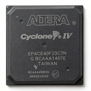
EP1K50FC484-1N - 50K-Gate ACEX-1K FPGA 250MHz 484-BGA | Intel
MPN: EP1K50FC484-1N ✗ End of Life| Qty | Unit Price | Extended |
|---|---|---|
| 1 | $38.5 | $38.50 |
| 10 | $34.2 | $342.00 |
| 100 | $28.9 | $2,890.00 |
| 500 | $24.6 | $12,300.00 |
| 1,000 | $21.4 | $21,400.00 |
EP1K50FC484-1N Overview
An FPGA (Field-Programmable Gate Array) is a programmable logic device that sits between a microcontroller and a custom ASIC in the semiconductor hierarchy: ASIC → FPGA → microcontroller → general-purpose processor. FPGAs integrate configurable logic blocks (LEs), programmable interconnect, and on-chip memory so engineers can implement arbitrary digital logic, DSP pipelines, glue logic, and bus interfaces without a custom mask set. The ACEX-1K family was the first Altera family to embed dedicated array blocks (EABs) for memory or arithmetic functions, and it targets glue-logic, bus-bridging, and low-to-mid volume custom logic designs.
Key features of the EP1K50FC484-1N include 360 Logic Array Blocks (LABs), 12 Embedded Array Blocks (EABs) providing 40,960 RAM bits, multi-standard I/O support (LVTTL, LVCMOS, PCI, GTL+, SSTL-2), in-system programmability via the JTAG-compliant IEEE Std. 1149.1 interface, and 4 dedicated clock inputs with up to 6 global clock networks. The 484-FBGA package exposes 249 user I/O, giving designers ample headroom for parallel buses and memory interfaces while fitting into a surface-mount footprint.
From an architectural standpoint, each Logic Element in ACEX-1K contains a 4-input look-up table (LUT), a programmable register, and a carry chain for arithmetic. The EABs can be configured as 4,096-bit RAM or ROM blocks, allowing efficient implementation of FIFOs, lookup tables, and small algorithmic coefficient stores. The device is configured using SRAM-based configuration cells, so it loads its bitstream on every power-up from a serial PROM, JTAG, or controller.
Typical applications include communications infrastructure glue logic, peripheral-bus bridging (e.g., PCI to local bus), industrial control and instrumentation, low-volume custom DSP pre/post-processing, and test-and-measurement backplanes. The wide I/O count also suits multi-channel data-acquisition front ends and protocol-conversion cards where multiple asynchronous interfaces must be absorbed in a single device.
When designing with the EP1K50FC484-1N, plan for the 2.5 V VCCINT core rail (separate from VCCIO for I/O banks), provide a configuration source (serial configuration PROM or JTAG), and respect the FBGA-484 routing rules (escape routing on multiple layers, microvia stack if possible). The device is commercial temperature grade (0 °C to +70 °C); industrial or military temperature grades carry the "I" or "MIL" speed-grade suffix.
This page synthesizes distributor pricing, drop-in same-package alternatives, and practical design notes that complement, rather than duplicate, the manufacturer datasheet.
Drop-in alternatives for EP1K50FC484-1N — same package, pin-to-pin compatible. Different-package parts requiring PCB rework are excluded.
Variants in this series
Same-series models that are drop-in compatible with EP1K50FC484-1N (same form factor and footprint) — differing in Speed Grade, Package, Process Technology, Configuration Method, Operating Temperature.
Quick Comparison Tool — Select alternative parts for side-by-side comparison:
EP1K50FC484-1
✅ Drop-In✓ In Stock
$26.4 / Unit
View Datasheet →EP1K50FC484-2N
✅ Drop-In✓ In Stock
$26.4 / Unit
View Datasheet →EP1K50FC484-3N
✅ Drop-In✓ In Stock
$19.5 / Unit
View Datasheet →EP1K100FC484-1N
✅ Drop-In✓ In Stock
$58.4 / Unit
View Datasheet →EP1K100FC484-2N
✅ Drop-In✓ In Stock
$58.4 / Unit
View Datasheet →EP1K50FC484-1N Maximum Ratings & Electrical Characteristics
| Family | ACEX-1K |
| Manufacturer | Intel (formerly Altera) |
| Logic Elements (LEs) | 2,880 |
| Typical System Gates | 50,000 |
| Maximum User I/O Pins | 249 |
| Logic Array Blocks (LABs) | 360 |
| Embedded Array Blocks (EABs) | 12 |
| Embedded Memory (Bits) | 40,960 |
| Maximum Internal Clock Frequency | 250 MHz |
| Process Technology | 0.22 µm CMOS |
| Core Supply Voltage (VCCINT) | 2.5 V |
| Package | 484-ball FineLine BGA (FBGA) |
| Mounting Type | Surface Mount |
| Speed Grade | -1 (commercial) |
| Configuration Method | SRAM, JTAG (IEEE 1149.1) |
| RoHS Status | Compliant (lead-free "N" suffix) |
EP1K50FC484-1N 484-ball fineline bga (fbga) Pin Configuration Guide
Pin configuration for EP1K50FC484-1N (484-ball fineline bga (fbga) package). This digital IC includes GPIO, communication interfaces (UART, SPI, I2C), and power pins. Refer to the manufacturer datasheet for alternate pin functions and configuration options. Essential for embedded system design and PCB layout.

No detailed pinout data available for EP1K50FC484-1N.
Refer to the datasheet for full pin configuration.
Typical Applications
EP1K50FC484-1N is suitable for 6 applications: Communications Infrastructure Glue Logic, Industrial Control & Instrumentation, PCI / Local-Bus Bridging, Test & Measurement Backplanes, Low-Volume Custom DSP Pre/Post-Processing, Legacy Peripheral & Protocol-Conversion Cards.
Communications Infrastructure Glue Logic
The EP1K50FC484-1N's 50K gates and 249 user I/O in a 484-FBGA package make it a strong fit for telecom glue-logic cards that bridge standard buses and protocol converters. Its 250 MHz internal clock and PCI-compatible I/O let it absorb protocol adaptation between legacy TDM backplanes and packet-based fabrics without external bus switches. The 12 EABs (40,960 bits of dual-port RAM) handle small cell buffers and lookup tables in place of an external SRAM, reducing BOM cost. Compared with a CPLD, the EP1K50 absorbs wider parallel buses in one device.
Recommended
Industrial Control & Instrumentation
With 249 I/O pins and multi-standard I/O support (3.3 V LVTTL/LVCMOS, PCI, GTL+), the EP1K50FC484-1N is well-suited to industrial controllers that must interface parallel ADC/DAC banks, motor-control PWMs, and field-bus bridges in a single device. The 2.5 V core is tolerant of industrial 24 V supply rails after step-down, and the JTAG boundary-scan interface simplifies in-system programming on the production line. The device is commercial-grade (0 °C to +70 °C); for harsher industrial thermal ranges, select the I-temp variant or migrate to Cyclone IV.
Recommended
PCI / Local-Bus Bridging
The EP1K50FC484-1N's PCI-compatible I/O pins and 50K-gate capacity let it act as a transparent bridge between a 32-bit/33 MHz PCI bus and a proprietary peripheral bus, eliminating the need for an expensive PCI bridge ASIC. Its 12 EABs (40,960 bits) can implement small FIFO buffers in dual-port mode, smoothing burst transfers across clock domains. The 484-FBGA package exposes enough user I/O to break out both 32-bit PCI and a 32-bit local bus simultaneously. Quartus IP cores provide ready-made PCI target controllers.
Recommended
Test & Measurement Backplanes
The EP1K50FC484-1N serves well in test-and-measurement backplanes where multiple parallel data streams (LVTTL/LVCMOS) must be multiplexed, framed, and forwarded to a host processor. The 360 LABs and 12 EABs support pattern generation, error counters, and small DSP pre-processing pipelines up to 250 MHz. The 484-FBGA package enables compact PCB layouts with controlled-impedance routing for high-speed LVDS-style signals. JTAG scan chains enable board-level boundary-scan test integration on production testers.
Recommended
Low-Volume Custom DSP Pre/Post-Processing
For low-volume designs requiring custom DSP pipelines (FIR filters, FFT pre-processing, codec rate conversion), the EP1K50FC484-1N delivers 50K gates and 12 EABs of memory at a fraction of ASIC NRE cost. The 250 MHz internal clock supports video-rate DSP at common pixel clock frequencies. Compared with a discrete DSP processor, the FPGA allows bit-width customization and parallel datapaths. Quartus DSP IP and Megafunctions simplify filter and FFT instantiation.
Recommended
Legacy Peripheral & Protocol-Conversion Cards
The EP1K50FC484-1N is a typical solution for legacy peripheral cards that must translate between obsolete parallel protocols (VME, ISA, PC/104) and modern serial interfaces. Its wide I/O count (249 pins) accommodates several legacy buses simultaneously, and its EAB-based dual-port RAM acts as a rate-matching buffer between asynchronous domains. For long-life-cycle industrial and defense systems that must remain in production for decades, the EP1K50FC484-1N's mature tooling (Quartus II) and broad second-source availability remain an advantage.
Recommended
Recommended Products Summary
Engineering reference data for EP1K50FC484-1N — comparison, design guidance, and compliance information.
Selection Guide
Comparison with Alternatives
| Parameter | This Product | EP1K50FC484-1 | EP1K50FC484-2N | EP1K50FC484-3N | EP1K100FC484-1N | EP1K100FC484-2N |
|---|---|---|---|---|---|---|
| Brand | Intel (formerly Altera) | Intel (formerly Altera) | Intel (formerly Altera) | Intel (formerly Altera) | Intel (formerly Altera) | Intel (formerly Altera) |
| Package | 484-FBGA (FineLine BGA) | 484-FBGA (same) | 484-FBGA (same) | 484-FBGA (same) | 484-FBGA (same) | 484-FBGA (same) |
| Family | ACEX-1K | ACEX-1K | ACEX-1K | ACEX-1K | ACEX-1K | ACEX-1K |
| Typical System Gates | 50,000 | 50,000 | 50,000 | 50,000 | 100,000 (+100%) | 100,000 (+100%) |
| Logic Elements | 2,880 | 2,880 | 2,880 | 2,880 | 4,992 (+73%) | 4,992 (+73%) |
| Embedded Memory (bits) | 40,960 | 40,960 | 40,960 | 40,960 | 49,152 (+20%) | 49,152 (+20%) |
| Maximum User I/O | 249 | 249 | 249 | 249 | 333 | 333 |
| Speed Grade | -1 | -1 | -2 (faster) | -3 (fastest) | -1 | -2 (faster) |
| Lead-Free / RoHS | Yes (N) | No (no N suffix) | Yes (N) | Yes (N) | Yes (N) | Yes (N) |
Key Differentiators
- Wide 249-I/O 484-FBGA package with embedded memory (vs EP1K30FC256-3N)
- Higher logic capacity in the same 484-FBGA footprint (vs EP1K50FC484-1N vs EP1K100FC484-1N)
- Mature Quartus II toolchain with abundant legacy IP (vs Xilinx Spartan-II XC2S50)
Design Notes
The EP1K50FC484-1N requires a 2.5 V VCCINT core supply separate from VCCIO I/O bank supplies. Estimate Iccint at approximately 5-15 mA per MHz of internal toggle rate plus static EAB/IO contribution; use a low-noise LDO such as an LT3021-2.5 or TPS7A45 followed by a 22 µF + 0.1 µF ceramic decoupling network. I/O bank VCCIO must match the chosen I/O standard (3.3 V LVTTL, 2.5 V LVCMOS, 3.3 V PCI, etc.).
The 484-FBGA package requires multilayer PCB escape routing. Use microvias (laser-drilled, 6 mil pad) on at least 4 routing layers if possible, with the top layer dedicated to fan-out and inner layers for signal routing. Keep all decoupling capacitors within 100 mils of their respective supply balls and stitch GND vias on every BGA corner ball. Controlled-impedance traces (50 Ω single-ended) are mandatory for clocks and high-speed I/O.
ACEX-1K FPGAs use SRAM configuration cells, so they must reconfigure on every power-up. Provide a configuration source: a serial configuration PROM (EPC2LC20 / EPC4 / EPC8) in PS or AS mode, JTAG, or a microcontroller driving DCLK/DATA. Failure to populate the configuration source results in a non-functional board. JTAG chain integrity (TCK, TMS, TDI, TDO) must be verified with the Quartus programmer before board bring-up.
The 484-FBGA package has a θJA of approximately 15-20 °C/W (with proper PCB thermal design). For typical designs running at moderate toggle rates, junction temperature rise above ambient is under 10 °C. For high-utilization designs (>80% LE usage, high EAB bandwidth), verify thermal performance in the Quartus PowerPlay tool and add thermal vias under the BGA if needed.
Compliance Information
RoHS / lead-free status inferred from the "N" suffix in the MPN per Altera / Intel naming convention. REACH, halogen-free, and conflict-mineral declarations are not present in the verified web data; consult Intel's product compliance declarations for confirmation.