メモリ価格は日々変動しています — サイト上の価格は市場に遅れている可能性があります。最新の見積もりについてはRFQを送信してください。
最新価格をリクエスト →
ラストタイムバイのお知らせ: MT68A512M32DF-28:A は生産終了が近づいています。最終注文日: お問い合わせ. 利用可能な代替部品を見る →
Micron Technology

MT68A512M32DF-28:A - GDDR7 16Gbit 28Gbps | Micron

部品番号: MT68A512M32DF-28:A ✗ 生産終了
在庫あり 1〜3営業日以内に発送
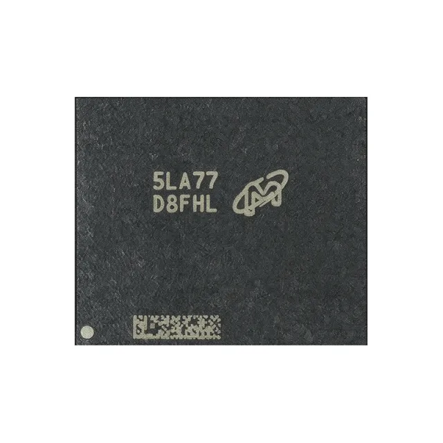
TFBGA (266-ball) Package -28 (28 Gbps) Speed SDRAM - GDDR7 Graphics DRAM Memory
開始価格 $41.0156 USD / 個
MOQ: 1 |
価格更新日: 2026-10-19
ボリューム価格
数量 単価 小計
1 $70.3125 $70.31
10 $50.7813 $507.81
100 $44.9219 $4,492.19
500 $42.9688 $21,484.40
1,000 $41.0156 $41,015.60
ℹ️ すべての価格はUSDです

MT68A512M32DF-28:A 概要

The Micron MT68A512M32DF-28:A is a 16Gbit (2GB) GDDR7 SDRAM graphics memory IC organized as 32-bit, operating at an effective data rate of 28 Gbps, housed in a 266-ball TFBGA (Fine-Pitch Ball Grid Array) package. As of 2026-10-11 the device has been designated End of Life by Micron alongside its 32 Gbps sibling MT68A512M32DF-32:A.

GDDR7 (Graphics Double Data Rate 7) is the latest generation of high-bandwidth graphics DRAM, succeeding GDDR6 and GDDR6X. Graphics DRAM sits within the broader memory hierarchy of volatile semiconductor memory: DRAM -> synchronous DRAM -> graphics DRAM -> GDDR family. Unlike DDR5, which prioritizes capacity per channel for CPUs, GDDR prioritizes aggregate bandwidth for GPU workloads, using wider per-device interfaces and PAM3 signaling introduced in the GDDR7 generation to raise per-pin data rates.

Key features of this device include the 16 Gbit density (2GB per chip), a 32-bit memory organization, and the 28 Gbps data rate, which matches the memory speed used by NVIDIA GeForce RTX 50 series cards such as the RTX 5060. The TFBGA package provides the short, controlled-impedance ball-out required for multi-gigabit signal integrity on graphics PCBs.

Architecturally, GDDR7 devices retain a SDRAM-style bank/row/column core while adopting PAM3 (3-level pulse amplitude modulation) I/O, which transmits three bits over two cycles and reduces the required clock frequency relative to NRZ signaling at equivalent bandwidth. This lowers power and EMI at 28 Gbps while supporting the trainability and error-tolerance features expected in modern GPU memory subsystems.

Typical applications include discrete graphics cards for gaming and workstation platforms, AI inference accelerators, video capture and broadcast equipment, and high-performance edge computing modules that require multi-hundred-GB/s memory bandwidth per chip.

A key design consideration is supply chain risk: this exact part was marked EOL in September 2026 as Micron shifts 2GB GDDR7 capacity to denser 24Gb (3GB) devices, so new designs should qualify alternate density or speed grades early and secure last-time-buy inventory.

This page synthesizes distributor listings, lifecycle reporting, and drop-in alternative guidance not found on a single manufacturer page, providing engineers a consolidated sourcing and design view.

ドロップイン代替品: MT68A512M32DF-28:A — 同一パッケージでピン互換。PCBの作り直しが必要な異なるパッケージの部品は除外されています。

クイック比較ツール — 並列比較する代替部品を選択:

MT68A512M32DF-32:A

speed grade only: 32 Gbps vs 28 Gbps (+14% data rate), same density/organization/pinout

📋 参考代替品(カタログ未掲載)

MT68A512M32DF-16:A

speed grade only: 16 Gbps vs 28 Gbps (-43% data rate), same footprint, usable when downclocked timings acceptable

📋 参考代替品(カタログ未掲載)

MT68A1G32DF-28:A

density 24Gbit (3GB) vs 16Gbit (2GB) (+50% capacity), same package family and speed grade; timing/BOM requalification required

📋 参考代替品(カタログ未掲載)

MT68A512M32DF-28:A 最大定格&電気的特性

メモリタイプ SDRAM - GDDR7 Graphics DRAM
メモリサイズ 16 Gbit (2 GB)
Memory Organization 32 (x32)
データレート 28 Gbps (per pin, effective)
インターフェース Parallel, GDDR7 (PAM3)
パッケージ TFBGA (266-ball)
実装タイプ Surface Mount
Technology DRAM
Supplier Device Package TFBGA
Base Part Number MT68A512M32DF
Speed Grade Suffix -28 (28 Gbps)
ライフサイクル状態 End of Life (announced September 2026)

MT68A512M32DF-28:A tfbga ピン配置ガイド

MT68A512M32DF-28:A (tfbga パッケージ) のピン配置。 このデジタルICには、GPIO、通信インターフェース (UART、SPI、I2C)、および電源ピンが含まれています。代替ピン機能と設定オプションについては、メーカーのデータシートを参照してください。組み込みシステム設計とPCBレイアウトに不可欠です。

MT68A512M32DF-28:A の tfbga パッケージピン配置図

詳細なピン配置データはありません: MT68A512M32DF-28:A.

詳細は データシート をご参照ください。

主な用途

MT68A512M32DF-28:A の用途: 6 件s: Discrete Graphics Cards (Gaming), AI Inference Accelerators, Video Capture and Broadcast Systems, Workstation Graphics, Networking and Security Appliances, Medical Imaging and Diagnostics.

🖥️

Discrete Graphics Cards (Gaming)

The MT68A512M32DF-28:A was designed for mainstream discrete gaming GPUs such as the NVIDIA GeForce RTX 5060, whose 28 Gbps memory clock matches this chip's speed grade exactly. Eight devices on a 256-bit bus provide 8GB and roughly 896 GB/s of aggregate bandwidth, sufficient for 1080p/1440p gaming frame buffers and textures. The PAM3-based GDDR7 interface reduces signaling power versus GDDR6 at equivalent bandwidth, which matters in power-constrained consumer card designs. Board designers place the chips around the GPU with matched-length fly-by routing; the trade-off is stricter eye-margin validation than GDDR6 layouts.

🧩

AI Inference Accelerators

Edge AI inference cards and accelerator modules use GDDR7 for its high bandwidth-per-watt and moderate cost versus HBM. The 28 Gbps data rate and 32-bit interface of the MT68A512M32DF-28:A deliver about 112 GB/s per device, letting a ring of four to eight chips feed transformer or CNN inference engines with several hundred GB/s. The 2GB per package suits models quantized to INT8/FP8. Designers should note that EOL status makes this part unsuitable for new accelerator programs; qualify the active 24Gb (3GB) GDDR7 devices instead, using this part only for sustaining existing builds.

📺

Video Capture and Broadcast Systems

Multi-channel 4K/8K video capture, frame synchronization, and broadcast playout systems require large, fast frame buffers. The MT68A512M32DF-28:A provides 16Gbit per chip; grouping several devices yields tens of gigabytes of frame store at over 100 GB/s per chip, enough to hold multiple uncompressed 4K60 frames with headroom for real-time overlays and format conversion. GDDR7's high bandwidth avoids the refresh bottlenecks of DDR4/DDR5 DIMM-based designs in embedded broadcast appliances. Since the part is EOL, broadcast OEMs should lock in last-time-buy quantities or migrate frame-store designs to the 3GB GDDR7 packages.

🖥️

Workstation Graphics

Professional workstation GPUs for CAD, DCC, and simulation use GDDR7 to combine near-HBM bandwidth with cost-effective capacity scaling. The 32-bit MT68A512M32DF-28:A allows board designers to populate 4, 8, or 16 chips for 8GB to 32GB frame buffers at 28 Gbps, delivering up to roughly 1.8 TB/s on a 512-bit design. Thermal design centers on the TFBGA package and its thermal interface to the card heatsink, keeping junction temperature within datasheet limits under sustained CUDA/OpenGL loads. Workstation vendors sustaining existing boards should verify remaining distributor stock, as 2GB GDDR7 supply narrowed after the September 2026 discontinuation.

🌐

Networking and Security Appliances

High-throughput network inspection, firewall, and 5G datapath appliances use GDDR7 as deep packet buffer memory. The 28 Gbps per-pin rate and 112 GB/s per device bandwidth of the MT68A512M32DF-28:A let a compact buffer subsystem absorb 400GbE line-rate bursts that would overflow DDR4-based buffering at equivalent latency. The PAM3 interface also reduces pin count and signal-integrity complexity versus GDDR6X. Because these appliances have long service lives and the chip is EOL, designers should size a last-time-buy to cover the appliance's support lifetime or requalify the buffer subsystem on active 3GB GDDR7 devices.

💊

Medical Imaging and Diagnostics

Ultrasound, digital radiography, and real-time diagnostic imaging pipelines demand very fast, deep line- and frame-buffer memory. A ring of MT68A512M32DF-28:A devices supplies multi-hundred-GB/s buffering that keeps beamforming, reconstruction, and display pipelines from starving at high frame rates. GDDR7's per-chip density simplifies buffer expansion: two chips give 4GB per imaging channel. Medical platforms carry long certification cycles, so the September 2026 EOL designation is significant - design teams should secure verified shelf stock for the certification period and document the MT68A1G32DF-class 3GB GDDR7 parts as the forward migration path.

おすすめ製品の概要

MT68A512M32DF-32:A Same-family faster speed grade (32 Gbps) for higher-end SKUs 使用用途: Discrete Graphics Cards (Gaming), Workstation Graphics XC7A100T-1FTG256C AMD 使用用途: Discrete Graphics Cards (Gaming) XCZU5CG-1SFVC784E AMD 使用用途: AI Inference Accelerators XCZU6CG-1FFVC900E AMD 使用用途: AI Inference Accelerators XC7K035T Kintex-7 class FPGA frame-buffer controller for video pipelines 使用用途: Video Capture and Broadcast Systems MT40A1G16TB-062E IT:F DDR4 companion for control-plane memory in broadcast appliances 使用用途: Video Capture and Broadcast Systems XC7VX485T Virtex-7 FPGA used in graphics subsystem prototyping 使用用途: Workstation Graphics ZL30772LFG7 Microchip Technology 使用用途: Networking and Security Appliances WGI210AT Intel 使用用途: Networking and Security Appliances ZSSC4151AE2R Renesas Electronics 使用用途: Medical Imaging and Diagnostics XC7S50-2CSGA324I AMD 使用用途: Medical Imaging and Diagnostics
What is the MT68A512M32DF-28:A?
The MT68A512M32DF-28:A is a Micron Technology 16Gbit (2GB) GDDR7 graphics SDRAM with a 32-bit organization and a 28 Gbps per-pin data rate, supplied in a 266-ball TFBGA package. According to Micron's official part-detail page, it belongs to the GDDR7 graphics memory family used primarily in discrete GPU designs such as the GeForce RTX 50 series.
What are the key specifications of MT68A512M32DF-28:A that engineers should know?
Key specifications: 16 Gbit (2GB) density, 32-bit I/O organization, 28 Gbps effective data rate (the -28 speed grade), GDDR7 protocol with PAM3 signaling, and a TFBGA ball-grid package. DigiKey lists it as a 'SDRAM - GDDR7 Memory IC 16Gbit 14 GHz', where 14 GHz corresponds to the PAM3 clock supporting 28 Gbps transfers. The part was designated End of Life by Micron in September 2026.
Is the MT68A512M32DF-28:A discontinued?
Yes. Micron marked the 2GB GDDR7 devices MT68A512M32DF-28:A (28 Gbps) and MT68A512M32DF-32:A (32 Gbps) as End of Life in its product catalog in September 2026, as reported by videocardz.com and Tom's Hardware. Supply from franchised distributors such as DigiKey, Mouser, Newark, and Avnet is now limited to existing stock, so new designs should plan a last-time-buy or qualify the denser 3GB (24Gbit) GDDR7 devices.
What is the best drop-in replacement for MT68A512M32DF-28:A?
The closest drop-in replacement is the same-package, same-footprint Micron MT68A512M32DF-32:A, a 16Gbit 2GB GDDR7 in the identical 32-bit TFBGA configuration that differs only in speed grade (32 Gbps vs 28 Gbps, a 14% data-rate increase). Because both are End of Life, designers should also evaluate Micron's 24Gb (3GB) GDDR7 devices, which change density and therefore require BOM and timing requalification rather than a pure drop-in.
What graphics cards use the MT68A512M32DF-28:A?
The MT68A512M32DF-28:A operates at 28 Gbps, matching the memory speed used by NVIDIA GeForce RTX 5060-class graphics cards, per videocardz.com reporting. Eight of these 2GB chips on a 256-bit bus yield 8GB of memory. Remaining stock has been used in limited quantities by third-party vendors in select RTX 50 series boards following the September 2026 discontinuation announcement.
What is the difference between MT68A512M32DF-28:A and MT68A512M32DF-32:A?
The only engineering difference is speed grade: the -28 variant runs at a 28 Gbps effective data rate, while the -32 variant runs at 32 Gbps. Both are 16Gbit (2GB), 32-bit GDDR7 devices in the same TFBGA package with the same pinout, so the -32 can be soldered on the same footprint and underclocked to 28 Gbps in a 28 Gbps design. Both were placed on End of Life in September 2026.
Is MT68A512M32DF-28:A pin compatible with GDDR6 or DDR5 memory?
No. GDDR7 devices use a different package ballout, protocol (PAM3 signaling), and command set from GDDR6/GDDR6X, and DDR5 is an entirely different memory class. A comparison with DDR5 parts such as the Micron MT40A1G16TB-062E IT:F shows fundamentally different bandwidth targets and organizations; GDDR7 cannot be socketed or soldered into a GDDR6 or DDR5 footprint. Memory controller support in the GPU is mandatory.
When should I choose MT68A512M32DF-28:A over a 3GB GDDR7 device?
Choose the MT68A512M32DF-28:A only for sustaining an existing PCBA whose layout, firmware timings, and bill of materials are already qualified for 2GB GDDR7 at 28 Gbps - for example a service or warranty replacement for RTX 5060-class boards. For new designs, Micron's 24Gb (3GB) GDDR7 devices provide more capacity per package and remain active, at the cost of a requalification cycle. Given the September 2026 EOL designation, starting a new design on this part is not advisable.
What is the equivalent Samsung or SK hynix GDDR7 for MT68A512M32DF-28:A?
Samsung and SK hynix also produce 2GB GDDR7 chips at comparable speeds, but no cross-brand part number could be verified as pin-to-pin drop-in for this Micron TFBGA device in the retrieved data. Cross-brand GDDR7 swaps require verifying ballout, timing registers, and GPU firmware compatibility. Consult Micron's part catalog and the GPU vendor's qualified vendor list before substituting, and treat any cross-brand change as a full requalification, not a drop-in.
Where can I download the MT68A512M32DF-28:A datasheet PDF?
The datasheet is available from Micron's official part-detail page at micron.com (search the GDDR7 part catalog for MT68A512M32DF-28:A), which links product specs and downloadable datasheets. Mirror copies are hosted by Octopart at octopart.com/datasheet/micron/MT68A512M32DF-28:A. Always prefer the Micron-hosted PDF since it carries the latest revision status, important for an EOL part where documentation updates may cease.
Where can I buy MT68A512M32DF-28:A and what is the price?
The MT68A512M32DF-28:A is listed by authorized distributors including DigiKey (ships today per its listing), Mouser, Newark, Avnet, and via TrustedParts and Octopart for price comparison. Because the part was designated EOL in September 2026, pricing is volatile and stock-limited; XAIPART lists quantity-break pricing as request-a-quote until verified current pricing is available. Expect above-standard-memory pricing as EOL supply narrows.
Is MT68A512M32DF-28:A in stock at DigiKey or Mouser?
The DigiKey listing shows 'Buy now, ships today', indicating in-stock availability at the time of listing, and Mouser also carries the part under its GDDR7 catalog. However, as an End-of-Life item announced in September 2026, stock is finite and will not be replenished. Buyers should confirm live inventory on the distributor pages and consider last-time-buy quantities given the 2GB GDDR7 supply narrowing reported in September 2026.
What is the data rate and bandwidth of the MT68A512M32DF-28:A?
The device runs at a 28 Gbps effective per-pin data rate on its 32-bit interface, giving roughly 112 GB/s of peak bandwidth per chip (28 Gbps x 32 bits / 8). DigiKey lists it as '16Gbit 14 GHz', reflecting the 14 GHz clock associated with GDDR7 PAM3 signaling at 28 Gbps. A 256-bit GPU bus using eight of these chips delivers approximately 896 GB/s aggregate bandwidth.
How should I design the PCB for MT68A512M32DF-28:A GDDR7 memory?
Design a controlled-impedance TFBGA fanout following the GPU vendor's GDDR7 layout guidelines: length-match the data groups, reference continuous ground planes, and place decoupling close to VDD/VDDQ balls. Because GDDR7 uses PAM3 signaling at 28 Gbps, eye-margin and equalization requirements are stricter than GDDR6. Use Micron's GDDR7 design resources and the GPU reference design rather than scaling a GDDR6 layout. Exact supply voltage and termination values should be taken from the Micron datasheet PDF.
What is the packaging and standard quantity for MT68A512M32DF-28:A?
Mouser lists the MT68A512M32DF-28:A in tray packaging ('TFBGA 2 CT' denoting 2 trays per container). GDDR7 BGA devices of this size are typically supplied in trays rather than tape-and-reel because of the 266-ball, ~14mm x 12mm-class body. Confirm exact tray quantity and packaging options with the distributor at order time, since EOL parts often shift to whatever packaging remains in warehouse stock.

エンジニアリング参考データ: MT68A512M32DF-28:A — 比較、設計ガイダンス、コンプライアンス情報。

選定ガイド

Choose the MT68A512M32DF-28:A only for sustaining or repairing existing boards already qualified for 2GB 28 Gbps GDDR7 - for example RTX 5060-class graphics cards and their industrial derivatives. If remaining stock is unavailable, the MT68A512M32DF-32:A is the first-choice drop-in: identical footprint and organization, running 14% faster and compatible with 28 Gbps timings. The MT68A512M32DF-16:A fits only bandwidth-relaxed designs and requires downclocked training. For new designs, do not select any 2GB GDDR7 part: Micron marked both speed grades End of Life in September 2026, so qualify the active 24Gb (3GB) GDDR7 devices (e.g., MT68A1G32DF-class) and budget for a requalification cycle. Cross-brand GDDR7 equivalents from Samsung or SK hynix exist at similar speeds but were not verified as pin-to-pin drop-ins, so treat any cross-brand swap as a full design change requiring GPU-controller firmware qualification.

代替品との比較

パラメータ この製品 MT68A512M32DF-32 MT68A512M32DF-16 MT68A1G32DF-28
Package TFBGA (266-ball) A: TFBGA (266-ball) - same A: TFBGA (266-ball) - same A: TFBGA (266-ball) - same
Brand Micron Technology A: Micron Technology A: Micron Technology A: Micron Technology
Density 16 Gbit (2 GB) A: 16 Gbit (2 GB) A: 16 Gbit (2 GB) A: 24 Gbit (3 GB)
Organization 32 (x32) A: 32 (x32) A: 32 (x32) A: 32 (x32)
Data Rate 28 Gbps A: 32 Gbps A: 16 Gbps A: 28 Gbps
Memory Type GDDR7 (PAM3) A: GDDR7 (PAM3) A: GDDR7 (PAM3) A: GDDR7 (PAM3)
Drop-in on Same Footprint - A: Yes - speed grade only A: Yes - requires downclocked timings A: Yes - timing/BOM requalification for new density

主な差別化要因

  • 28 Gbps speed grade aligned with RTX 5060-class GPUs (vs MT68A512M32DF-32:A)
  • Cost-efficient 2GB per package (vs MT68A1G32DF-28:A (3GB class))
  • Lower power and EMI via PAM3 signaling at 28 Gbps (vs MT68A512M32DF-16:A)
  • End-of-Life status reduces forward supply (vs MT68A1G32DF-28:A)

設計ノート

GDDR7 at 28 Gbps uses PAM3 signaling, which is substantially more sensitive to channel loss, crosstalk, and reference-plane discontinuities than GDDR6 NRZ at comparable rates. Follow the GPU vendor reference design for trace impedance, length matching within each data group, and via minimization under the TFBGA fanout. Eye-scan/equalization training must be re-validated whenever a different speed grade (e.g., -32:A) is populated, even though the footprint is identical.

GDDR7 devices use separate VDD and VDDQ rails; exact voltage values must be taken from the Micron MT68A512M32DF datasheet rather than assumed from GDDR6 values. Estimated: at multi-hundred-GB/s sustained workloads each 2GB package dissipates several watts, so plan a shared power stage with bulk and 0.1uF-class ceramic decoupling per device close to the balls. Verify per-rail current from the datasheet IDD specifications before finalizing the VRM.

Supply-chain pitfall: both the -28:A and -32:A 2GB GDDR7 parts were designated End of Life in September 2026, so designs qualified on them face finite supply. Do not start new layouts on this part; if a last-time-buy is taken, over-procure against expected service-life demand plus attrition. Also avoid mixing speed grades across a single memory bus unless the memory controller is trained per-device - use homogeneous populations on each channel.

Although the TFBGA body is small, sustained graphics workloads transfer significant heat into the PCB. Estimated: a multi-layer board with solid internal copper planes and thermal vias under the package spreads heat effectively; follow the GPU reference design's copper area and airflow assumptions. Verify junction temperature against the datasheet thermal resistance for the chosen stackup, and confirm thermal interface coverage over the populated memory array in card-level thermal simulation.

コンプライアンス情報

RoHS
Unknown
REACH
Unknown
AEC-Q100
鉛フリー
Unknown
ハロゲンフリー
Unknown
紛争鉱物
Unknown

Compliance details were not present in the retrieved distributor/manufacturer data. Micron typically publishes RoHS/REACH/conflict-minerals declarations per part on its product page; verify before regulatory sign-off.


データ検証日: 2026-10-11 — データはXAIPARTの部品エンジニアリングチームによって検証・管理されています

関連検索

MT68A512M32DF-28:A datasheet Micron MT68A512M32DF-28:A MT68A512M32DF-28:A buy price GDDR7 16Gbit 28Gbps 32-bit TFBGA MT68A512M32DF-28:A discontinued EOL MT68A512M32DF-28:A vs MT68A512M32DF-32:A MT68A512M32DF-28:A drop-in replacement Samsung SK hynix GDDR7 equivalent Micron 2GB RTX 5060 GDDR7 memory chip MT68A512M32DF 2GB GDDR7 last time buy what is MT68A512M32DF-28:A GDDR7 PAM3 28 Gbps memory bandwidth per chip

関連部品&用語

Micron Technology MT68A512M32DF-28:A MT68A512M32DF-32:A MT68A512M32DF-16:A MT68A1G32DF-28:A MT40A1G16TB-062E IT:F GDDR7 GDDR6 graphics DRAM DRAM SDRAM DDR5 PAM3 signaling TFBGA ball grid array NVIDIA GeForce RTX 5060 DigiKey Mouser Octopart End of Life last time buy memory bandwidth data rate Gbps AI inference accelerator
クイック見積RFQ
詳細をすべてご記入ください — 営業チームが24時間以内にご返信いたします
部品番号 メーカー パッケージ QTY 目標価格 小計
合計: $0.00 USD
✓
見積を送信しました!

24時間以内にメールでご返信いたします

1
RFQ送信済み
2
見積受領
3
注文済み
4
お支払い
5
発送済み
6
配達済み
RFQの詳細を表示
