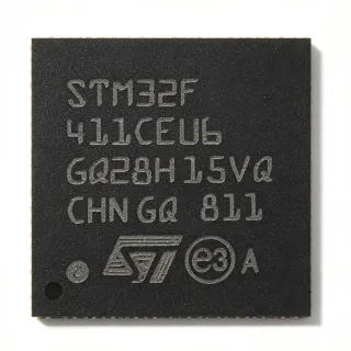
STM32F051C8U7 - 48MHz Cortex-M0 MCU 64KB Flash | STMicroelectronics
部品番号: STM32F051C8U7 ✓ 生産中| 数量 | 単価 | 小計 |
|---|---|---|
| 1 | $5.31 | $5.31 |
| 10 | $4.95 | $49.50 |
| 100 | $4.42 | $442.00 |
| 500 | $3.86 | $1,930.00 |
| 1,000 | $3.45 | $3,450.00 |
STM32F051C8U7 概要
A microcontroller (MCU) is a single-chip computer containing a processor core, program memory (Flash), working memory (SRAM), and configurable peripherals such as ADCs, timers, and communication interfaces. Within the embedded electronics hierarchy, MCUs sit between discrete microprocessors and application-specific standard products (ASSPs); the ARM Cortex-M family spans Cortex-M0/M0+ (smallest, lowest power) up to Cortex-M7 (highest performance). The STM32F0 family specifically targets 8/16-bit replacement, offering 32-bit performance at comparable prices and code density.
Key features of the STM32F051C8U7 include: 64 KB Flash / 8 KB SRAM, 1 × 12-bit ADC (1 µs, up to 16 channels), one 16-bit advanced-control timer for motor control, two USART, two I²C (SMBus/PMBus), two SPI (one multiplexed with I²S), HDMI CEC, USB 2.0 FS device, CAN 2.0B, and a 5-channel DMA. The device is offered in LQFP48, UFQFPN48, and WLCSP36 packages; the U7 suffix denotes the UFQFPN48 7×7 mm option. The industrial-grade temperature range is −40 °C to +105 °C.
The architecture is a Cortex-M0 core with single-cycle I/O access via a multi-AHB bus matrix, a 4-channel DMA controller, and a low-voltage 1.2 V internal regulator. The 12-bit ADC samples at 1 MSPS with configurable channel-scan and hardware oversampling; the advanced-control timer supports complementary PWM outputs with programmable dead-time, making it ideal for 3-phase motor control. The integrated USB 2.0 FS device and CAN 2.0B peripheral remove the need for external transceivers in many designs.
Typical applications include low-cost motor drives (BLDC, PMSM, brushed DC), home appliances and small white goods, USB peripherals and human-interface devices, HVAC controllers, sensor hubs, lighting controls, and 8/16-bit MCU replacement. The combination of CAN, USB, and a 16-bit motor-control timer in a single die makes the STM32F051C8U7 a strong fit for automotive body and chassis modules (non-safety-rated), as well as industrial PLCs and field sensors.
When designing with this device, note that the 48-pin UFQFPN package leaves a tighter analog pin budget than the 64-pin LQFP variant - plan your GPIO and peripheral mapping early. The internal 8 MHz RC oscillator is trimmed to ±1% over temperature, but USB and CAN require the external 12 MHz HSE crystal for jitter compliance.
ドロップイン代替品: STM32F051C8U7 — 同一パッケージでピン互換。PCBの作り直しが必要な異なるパッケージの部品は除外されています。
クイック比較ツール — 並列比較する代替部品を選択:
STM32F051C8U6
✅ ドロップイン📋 参考代替品(カタログ未掲載)
STM32F051C6U7
✅ ドロップイン📋 参考代替品(カタログ未掲載)
STM32F051C8U7TR
✅ ドロップイン📋 参考代替品(カタログ未掲載)
STM32F051C8U7 最大定格&電気的特性
| Core Architecture | ARM Cortex-M0 32-bit RISC |
| Maximum CPU Clock | 48 MHz |
| Program Memory (Flash) | 64 KB (64K x 8) |
| SRAM | 8 KB |
| Operating Voltage Range | 2.0 V to 3.6 V |
| パッケージ | 48-UFQFPN (7x7 mm) exposed pad |
| ADC | 1 × 12-bit, 1 µs conversion, up to 16 channels |
| Timers | Up to 11 timers including 1 advanced-control (motor-control PWM) |
| DMA Channels | 5 channels |
| Communication Interfaces | 2 × USART, 2 × I²C (SMBus/PMBus), 2 × SPI (one with I²S), HDMI CEC, USB 2.0 FS device, CAN 2.0B |
| 動作温度 | -40 °C to +105 °C (industrial grade) |
| Internal RC Oscillator | 8 MHz, ±1% accuracy |
| I/O Pins | Up to 39 fast GPIOs |
| 実装タイプ | Surface Mount |
| MSLレベル | 3 (168 hours) |
| RoHS ステータス | Compliant |
STM32F051C8U7 ピン構成
| ピン 1 | PB8 — GPIO/TIM16_CH1/CAN_RX |
| ピン 2 | PB9 — GPIO/IR_OUT/CAN_TX |
| ピン 3 | VSS — Digital ground |
| ピン 4 | VDD — Digital power 2.0-3.6 V |
| ピン 5 | OSC_IN — HSE crystal oscillator input |
| ピン 6 | OSC_OUT — HSE crystal oscillator output |
| ピン 7 | NRST — Reset input, active low |
| ピン 8 | VSSA — Analog ground |
| ピン 9 | VDDA — Analog power 2.0-3.6 V |
| ピン 10 | PA0 — GPIO/ADC_IN0/TIM2_CH1_ETR |
| ピン 11 | PA1 — GPIO/ADC_IN1/TIM2_CH2 |
| ピン 12 | PA2 — GPIO/USART1_TX/ADC_IN2 |
| ピン 13 | PA3 — GPIO/USART1_RX/ADC_IN3 |
| ピン 14 | PA4 — GPIO/SPI1_NSS/ADC_IN4 |
| ピン 15 | PA5 — GPIO/SPI1_SCK/ADC_IN5 |
| ピン 16 | PA6 — GPIO/SPI1_MISO/ADC_IN6 |
| ピン 17 | PA7 — GPIO/SPI1_MOSI/ADC_IN7 |
| ピン 18 | PB0 — GPIO/ADC_IN8/TIM3_CH3 |
| ピン 19 | PB1 — GPIO/ADC_IN9/TIM3_CH4 |
| ピン 20 | PB2 — GPIO/BOOT0 (must be tied low for normal boot) |
| ピン 21 | PB10 — GPIO/I2C2_SCL/USART3_TX |
| ピン 22 | PB11 — GPIO/I2C2_SDA/USART3_RX |
| ピン 23 | VSS — Digital ground |
| ピン 24 | VDD — Digital power 2.0-3.6 V |
| ピン 25 | PB12 — GPIO/SPI2_NSS/TIM1_BKIN |
| ピン 26 | PB13 — GPIO/SPI2_SCK/TIM1_CH1N |
| ピン 27 | PB14 — GPIO/SPI2_MISO/TIM1_CH2N |
| ピン 28 | PB15 — GPIO/SPI2_MOSI/TIM1_CH3N |
| ピン 29 | PA8 — GPIO/USART1_CK/TIM1_CH1 |
| ピン 30 | PA9 — GPIO/USART1_TX/TIM1_CH2 |
| ピン 31 | PA10 — GPIO/USART1_RX/TIM1_CH3 |
| ピン 32 | PA11 — GPIO/USB_DM/CAN_RX |
| ピン 33 | PA12 — GPIO/USB_DP/CAN_TX |
| ピン 34 | PA13 — GPIO/SWDIO (programming data) |
| ピン 35 | VSS — Digital ground |
| ピン 36 | VDD — Digital power 2.0-3.6 V |
| ピン 37 | PA14 — GPIO/SWCLK (programming clock) |
| ピン 38 | PA15 — GPIO/SPI1_NSS/TIM2_CH1_ETR |
| ピン 39 | PB3 — GPIO/SPI1_SCK/TIM2_CH2 |
| ピン 40 | PB4 — GPIO/SPI1_MISO/TIM3_CH1 |
| ピン 41 | PB5 — GPIO/SPI1_MOSI/TIM3_CH2 |
| ピン 42 | PB6 — GPIO/I2C1_SCL/USART1_TX |
| ピン 43 | PB7 — GPIO/I2C1_SDA/USART1_RX |
| ピン 44 | BOOT0 — Boot mode select (tie low for flash boot) |
| ピン 45 | PB8 — GPIO/TIM16_CH1 (alt) |
| ピン 46 | VSS — Digital ground |
| ピン 47 | VDD — Digital power 2.0-3.6 V |
| ピン 48 | VSS — Digital ground (exposed pad) |
主な用途
STM32F051C8U7 の用途: 6 件s: Low-Voltage BLDC / PMSM Motor Control, USB HID Peripherals and PC Accessories, CAN Node for Automotive Body and Chassis, Home Appliance Control Board, Sensor Hub and HVAC Transmitter, 8-Bit / 16-Bit MCU Replacement.
Low-Voltage BLDC / PMSM Motor Control
The STM32F051C8U7's 16-bit advanced-control timer with complementary PWM outputs and programmable dead-time drives a 3-phase inverter directly, while the 1 µs 12-bit ADC samples back-EMF and current sense resistors in the same instruction window. Its Cortex-M0 core at 48 MHz executes sensorless field-oriented-control (FOC) loops at switching frequencies up to 20 kHz with comfortable headroom, and the CAN 2.0B peripheral supports industrial fieldbus (CANopen, DeviceNet) integration without an external controller. The 48-pin UFQFPN keeps the board footprint under 50 mm², which suits small appliance and fan-controller designs.
おすすめ
USB HID Peripherals and PC Accessories
The STM32F051C8U7's integrated USB 2.0 Full-Speed device controller with on-chip pull-up removes the need for an external PHY, and the 64 KB Flash comfortably hosts USB HID, CDC, or vendor-class stacks. The 48 MHz Cortex-M0 handles polling at 1 kHz with cycles to spare for debouncing, LED animations, and command processing. Its low active current (around 7 mA at 48 MHz) and suspend-mode support (under 2 µA) make the device a strong fit for USB keyboards, mice, game controllers, and small data-acquisition dongles that must meet USB suspend-current budgets.
おすすめ
CAN Node for Automotive Body and Chassis
The STM32F051C8U7's bxCAN 2.0B peripheral with hardware acceptance filters and a 5-channel DMA controller offloads message handling from the Cortex-M0 core, making it well suited to automotive body and chassis nodes such as seat controllers, window lifters, mirror modules, and HVAC flaps. The 64 KB Flash stores CANopen or J1939 stacks, and the 12-bit ADC reads sensor inputs (position, temperature) with 1 µs settling. Operating at -40 °C to +105 °C across a 2.0-3.6 V supply range, the part is suitable for non-safety-rated body modules though it is not AEC-Q100 qualified.
おすすめ
Home Appliance Control Board
The combination of motor-control PWM, multiple communication interfaces (I²C for sensor hubs, UART for HMI displays, SPI for external flash), and an industrial temperature range makes the STM32F051C8U7 a strong choice for washing-machine motor boards, refrigerator compressors, and small kitchen-appliance controllers. The 12-bit ADC with up to 16 channels supports thermistor, current-sense, and water-level inputs, while the 64 KB Flash hosts IEC 60730 Class B safety library code without squeezing application logic. The UFQFPN package drops into compact PCBAs where 48-pin LQFPs would be too tall.
おすすめ
Sensor Hub and HVAC Transmitter
The two I²C buses on the STM32F051C8U7 can host multiple temperature, humidity, and pressure sensors simultaneously, while the 12-bit ADC reads analog front-end outputs from thermocouples, RTDs, or 4-20 mA loops. The DMA controller streams ADC conversions into RAM without CPU intervention, and the 48 MHz Cortex-M0 runs the application loop (filter, linearize, transmit) with sub-millisecond latency. This combination suits industrial HVAC transmitters, building-automation sensor nodes, and small environmental data loggers that need CAN or RS-485 uplink.
おすすめ
8-Bit / 16-Bit MCU Replacement
The STM32F051C8U7 is positioned as a 32-bit upgrade path for legacy 8-bit (8051, PIC16, AVR) and 16-bit (MSP430, PIC24) designs. The Cortex-M0 delivers roughly 0.9 DMIPS/MHz, around 12-20x the throughput of a comparable 8-bit MCU at the same clock, and the 64 KB Flash stores legacy code plus new features. The 48-pin UFQFPN footprint is similar in size to a 44-pin LQFP used by many 16-bit parts, easing PCB reuse. The peripheral mix (USB, CAN, ADC, motor-control timer) often replaces two or three external 8-bit MCUs in a single chip.
おすすめ
おすすめ製品の概要
エンジニアリング参考データ: STM32F051C8U7 — 比較、設計ガイダンス、コンプライアンス情報。
選定ガイド
代替品との比較
| パラメータ | この製品 | STM32F051C8T6 | STM32F051C8U6 | STM32F051C6U7 | STM32F051C8U7TR | STM32F030C8T6TR |
|---|---|---|---|---|---|---|
| Package | UFQFPN-48 (7x7 mm) | LQFP-48 (7x7 mm) | UFQFPN-48 (7x7 mm) - same | UFQFPN-48 (7x7 mm) - same | UFQFPN-48 (7x7 mm) - same | LQFP-48 (7x7 mm) |
| Brand | STMicroelectronics | STMicroelectronics | STMicroelectronics | STMicroelectronics | STMicroelectronics | STMicroelectronics |
| Flash Memory | 64 KB | 64 KB | 64 KB | 32 KB (-50%) | 64 KB | 64 KB |
| SRAM | 8 KB | 8 KB | 8 KB | 4 KB (-50%) | 8 KB | 8 KB |
| CPU Core | Cortex-M0 @ 48 MHz | Cortex-M0 @ 48 MHz | Cortex-M0 @ 48 MHz | Cortex-M0 @ 48 MHz | Cortex-M0 @ 48 MHz | Cortex-M0 @ 48 MHz |
| USB 2.0 FS Device | Yes | Yes | Yes | Yes | Yes | No |
| CAN 2.0B | Yes | Yes | Yes | Yes | Yes | No |
| Operating Temperature | -40C to +105C (U7 grade) | -40C to +85C (T6 grade) | -40C to +85C (U6 grade) | -40C to +105C | -40C to +105C | -40C to +85C |
| Unit Price (1 pc, USD) | $5.31 | $4.95 | $4.50 | $4.20 | $5.31 | $2.85 |
主な差別化要因
- Motor-control advanced timer integrated (vs STM32F030C8T6TR)
- Native USB 2.0 FS device and CAN 2.0B (vs STM32F030C8T6TR)
- Industrial -40C to +105C temperature grade (vs STM32F051C8T6)
設計ノート
Decouple each VDD/VSS pair with 100 nF ceramic plus a shared 4.7 µF bulk cap placed within 5 mm of the pins. Place VDDA/VSSA decoupling (100 nF + 1 µF) close to the analog pins to keep ADC noise below 1 LSB at 1 MSPS. Estimated: at 48 MHz active mode the core draws ~7 mA from VDD, so the 4.7 µF bulk must source the 7 mA for at least 1 µs without sagging below 2.0 V - a 4.7 µF X5R cap with 0.1 Ω ESR meets this easily.
The 48-pin UFQFPN has a thermal resistance (theta-JA) of approximately 35 °C/W on a standard 2-layer JEDEC test board. With the typical 30 mW active dissipation, junction rise is ~1 °C above ambient - thermal management is not a concern. Solder the exposed pad to a continuous ground copper pour (at least 25 mm²) to achieve the rated thermal performance; without this the die may overheat in enclosed appliances.
Keep the HSE crystal traces within 5 mm of the OSC_IN/OSC_OUT pins, with ground guard traces on both sides. Place the HSE load capacitors (typically 10-20 pF) as close to the crystal as possible. For USB applications, route the USB_DM/USB_DP pair as a 90-ohm differential with no stubs and place the 1.5 kΩ pull-up on USB_DP close to the MCU pin, not the connector. Route the analog ADC inputs away from switching nodes (PWM outputs) by at least 5 mm or guard with ground pour.
Do not leave BOOT0 floating - tie it to VSS through a 10 kΩ resistor for normal Flash boot. Failing to do so can result in the part entering System Memory bootloader mode after noise or reset glitches. When using USB without an external 12 MHz HSE, the HSI48 internal oscillator is too jittery for USB compliance - always use an external crystal or ceramic resonator for USB designs. The CAN peripheral also requires HSE for stable bit timing above 125 kbps.
コンプライアンス情報
RoHS and REACH compliant per STMicroelectronics product page. Not AEC-Q100 qualified - the part is rated industrial -40C to +105C but does not carry the automotive Q100 certification. For AEC-Q100 applications, refer to the STM32F0 automotive-grade variants (STM32F051C8U7 with automotive ordering code). Halogen-free per IEC 61249-2-21.