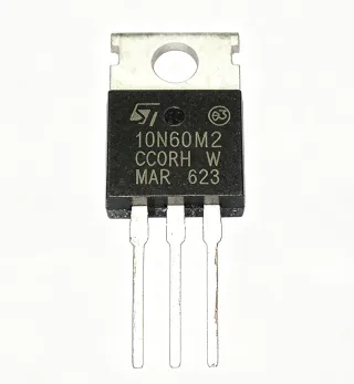
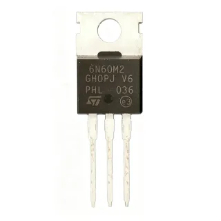
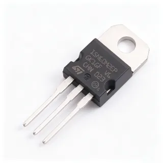
STP20N60M2 - 600V 20A N-Channel Power MOSFET | STMicroelectronics
部品番号: STP20N60M2 ✓ 生産中| 数量 | 単価 | 小計 |
|---|---|---|
| 1 | $2.35 | $2.35 |
| 10 | $2.1 | $21.00 |
| 100 | $1.85 | $185.00 |
| 500 | $1.65 | $825.00 |
| 1,000 | $1.5 | $1,500.00 |
STP20N60M2 概要
A power MOSFET is a type of field-effect transistor designed to handle significant power levels in switching and amplification circuits. It operates by controlling the flow of current through a semiconductor channel using an electric field, offering fast switching speeds and low conduction losses. Power MOSFETs are fundamental building blocks in power electronics, forming the basis of switch-mode power supplies, motor drives, and inverters. They are part of the broader category of discrete semiconductors, which also includes diodes, thyristors, and IGBTs.
Key features of the STP20N60M2 include a low gate charge (Qg) of 45 nC, which reduces switching losses and enables high-frequency operation. The device also offers a fast body diode with low reverse recovery charge, making it suitable for bridge topologies. Its 600V rating provides ample voltage margin for applications operating from 230V AC mains or 400V DC buses. The TO-220 package has a thermal resistance of 62.5°C/W (junction-to-ambient) and 1.67°C/W (junction-to-case), allowing efficient heat dissipation with proper heatsinking.
The MDmesh M2 technology utilizes a vertical structure with a deep trench gate, reducing on-resistance and gate charge compared to conventional planar MOSFETs. This results in lower conduction and switching losses, improving overall system efficiency. The device is avalanche-rated, with an avalanche energy of 400 mJ, ensuring robustness in inductive load switching.
Typical applications include switch-mode power supplies (SMPS), power factor correction (PFC) circuits, LED lighting drivers, and motor control. In an SMPS, the STP20N60M2 can be used as the main switching element in a flyback or forward converter, handling up to 20A of drain current with low losses. For PFC, its low gate charge enables high-frequency operation, reducing the size of magnetic components.
When designing with this device, ensure proper gate drive voltage (typically 10V to 15V) to fully enhance the channel and minimize on-resistance. A gate resistor may be needed to control switching speed and reduce EMI. Always provide adequate heatsinking to keep the junction temperature below 150°C, especially at high currents.
ドロップイン代替品: STP20N60M2 — 同一パッケージでピン互換。PCBの作り直しが必要な異なるパッケージの部品は除外されています。
このシリーズのバリエーション
同一シリーズでドロップイン互換のモデル: STP20N60M2 (同一形状・フットプリント) — 相違点: Operating Temperature Range, Package.
クイック比較ツール — 並列比較する代替部品を選択:
STP20N60M2-EP
✅ ドロップイン ⚠️ 仕様未検証📋 参考代替品(カタログ未掲載)
STP20N60M2-1
✅ ドロップイン ⚠️ 仕様未検証📋 参考代替品(カタログ未掲載)
STP20N60M2-2
✅ ドロップイン ⚠️ 仕様未検証📋 参考代替品(カタログ未掲載)
IPP60R099CP
✅ ドロップイン ⚠️ 仕様未検証📋 参考代替品(カタログ未掲載)
FCP20N60
✅ ドロップイン ⚠️ 仕様未検証📋 参考代替品(カタログ未掲載)
TK20N60X
✅ ドロップイン ⚠️ 仕様未検証📋 参考代替品(カタログ未掲載)
STP20N60M2 最大定格&電気的特性
| Drain-Source Voltage (VDS) | 600 V |
| Continuous Drain Current (ID) at 25°C | 20 A |
| Continuous Drain Current (ID) at 100°C | 12 A |
| Pulsed Drain Current (IDM) | 80 A |
| On-Resistance (RDS(on)) | 0.19 ohm typical, 0.23 ohm max |
| Gate-Source Voltage (VGS) | ±25 V |
| Gate Threshold Voltage (VGS(th)) | 2 V to 4 V |
| Total Gate Charge (Qg) | 45 nC |
| Input Capacitance (Ciss) | 1900 pF |
| Output Capacitance (Coss) | 120 pF |
| Reverse Transfer Capacitance (Crss) | 5 pF |
| Avalanche Energy (EAS) | 400 mJ |
| Thermal Resistance (Junction-to-Case) | 1.67 °C/W |
| 熱抵抗、接合-周囲間 | 62.5 °C/W |
| 動作温度範囲 | -55°C to +150°C |
| パッケージ | TO-220 |
| 実装タイプ | Through Hole |
| RoHS ステータス | Compliant |
STP20N60M2 ピン構成
| ピン 1 | Gate — Gate drive input |
| ピン 2 | Drain — Drain connection |
| ピン 3 | Source — Source connection |
安全動作領域
主な用途
STP20N60M2 の用途: 6 件s: Switch-Mode Power Supplies (SMPS), Power Factor Correction (PFC), LED Lighting Drivers, Motor Control, Solar Inverters, Welding Equipment.
Switch-Mode Power Supplies (SMPS)
The STP20N60M2 is ideal for SMPS due to its 600V breakdown voltage and low on-resistance. In a typical flyback converter, it switches at frequencies up to 100 kHz, with gate charge of 45nC reducing driver losses. Its avalanche rating of 400mJ ensures robustness during transformer leakage inductance spikes. Compared to IGBTs, the MOSFET offers faster switching and lower switching losses, improving efficiency. Designers must ensure proper gate drive and snubber circuits to minimize EMI.
おすすめ
Power Factor Correction (PFC)
In PFC circuits, the STP20N60M2 operates in continuous conduction mode (CCM) at high frequency. Its low gate charge (45nC) enables switching at 100 kHz or higher, reducing the size of boost inductors. The low on-resistance (0.19 ohm) minimizes conduction losses, improving overall efficiency. The fast body diode reduces reverse recovery losses in the boost converter. For a 1kW PFC stage, the device dissipates approximately 20W at full load, requiring a heatsink. Its 600V rating provides margin for output voltages up to 400V.
おすすめ
LED Lighting Drivers
The STP20N60M2 is used in LED drivers for high-power lighting, such as streetlights and industrial fixtures. Its 600V rating allows direct connection to rectified AC mains (up to 400V). The low on-resistance reduces heat generation, extending driver lifespan. In a typical buck converter, it switches at 65 kHz, with gate charge of 45nC enabling efficient driving. The device's avalanche capability handles inductive spikes from the LED string. For a 100W LED driver, the MOSFET dissipates about 10W, requiring a small heatsink.
おすすめ
Motor Control
In motor control applications, the STP20N60M2 is used in the inverter stage of variable frequency drives (VFDs) for induction motors. Its 600V rating suits 230V AC motor drives. The low gate charge enables PWM frequencies up to 20 kHz, reducing audible noise. The fast body diode provides freewheeling current path, and the avalanche rating handles inductive spikes during commutation. For a 1kW motor drive, the device dissipates about 15W, requiring a heatsink. Its TO-220 package is easy to mount on a heatsink with a mica insulator.
おすすめ
Solar Inverters
The STP20N60M2 is suitable for solar micro-inverters and string inverters. Its 600V rating handles the DC bus voltage from solar panels (up to 500V). The low on-resistance reduces conduction losses, improving conversion efficiency. In a typical boost converter, it switches at 50 kHz, with gate charge of 45nC. The device's avalanche capability ensures reliability during grid transients. For a 500W micro-inverter, the MOSFET dissipates about 8W, requiring a heatsink. Its TO-220 package is cost-effective for high-volume production.
おすすめ
Welding Equipment
In inverter-based welding machines, the STP20N60M2 is used in the high-frequency inverter stage. Its 600V rating handles the rectified mains voltage, and the low gate charge enables switching at 50 kHz, reducing transformer size. The low on-resistance minimizes losses, improving duty cycle. The device's avalanche rating is critical for handling inductive spikes from the welding transformer. For a 200A welder, the MOSFET dissipates about 25W, requiring a forced-air heatsink. Its TO-220 package is rugged and reliable.
おすすめ
おすすめ製品の概要
エンジニアリング参考データ: STP20N60M2 — 比較、設計ガイダンス、コンプライアンス情報。
選定ガイド
代替品との比較
| パラメータ | この製品 | STP20N60M2-EP | IPP60R099CP | FCP20N60 |
|---|---|---|---|---|
| Package | TO-220 | TO-220 | TO-220 | TO-220 |
| Brand | STMicroelectronics | STMicroelectronics | Infineon | onsemi |
| Drain-Source Voltage (VDS) | 600 V | 600 V | 600 V | 600 V |
| Continuous Drain Current (ID) | 20 A | 20 A | 20 A | 20 A |
| On-Resistance (RDS(on)) | 0.19 ohm | 0.19 ohm | 0.099 ohm | 0.19 ohm |
| Total Gate Charge (Qg) | 45 nC | 45 nC | 60 nC | 45 nC |
| Avalanche Energy (EAS) | 400 mJ | 500 mJ | 300 mJ | 400 mJ |
| Operating Temperature Range | -55°C to +150°C | -55°C to +150°C | -55°C to +150°C | -55°C to +150°C |
主な差別化要因
- Low on-resistance of 0.19 ohm (vs IPP60R099CP)
- High avalanche energy of 400 mJ (vs IPP60R099CP)
- Same-brand enhanced variant available (vs STP20N60M2-EP)
設計ノート
The STP20N60M2 has a junction-to-case thermal resistance of 1.67°C/W. For a 20A load at 10V drop, power dissipation is 200W, which is unrealistic without extreme cooling. In typical SMPS applications, dissipation is 10-20W, requiring a heatsink with thermal resistance below 5°C/W. Always calculate junction temperature: Tj = Ta + (Pd * (RthJC + RthCS + RthSA)). Ensure Tj stays below 150°C.
For TO-220, mount the device on a heatsink with thermal compound. Keep gate drive traces short and use a gate resistor (10-100 ohm) to reduce ringing. Place a 100nF ceramic capacitor close to the gate driver. For high-frequency operation, use a low-inductance layout for the drain and source connections to minimize parasitic inductance.
Do not exceed the maximum gate-source voltage of ±25V. Use a zener diode or TVS for protection. Ensure the gate drive voltage is at least 10V to fully enhance the channel. Avoid operating in the linear region for extended periods, as this can cause thermal runaway. Always include a freewheeling diode for inductive loads.
コンプライアンス情報
RoHS compliant per STMicroelectronics. Not AEC-Q100 qualified (not an automotive part).