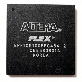
XC6SLX150-N3FG484C - Spartan-6 LX FPGA, 338 I/O | AMD
部品番号: XC6SLX150-N3FG484C ✓ 生産中XC6SLX150-N3FG484C 概要
An FPGA is a semiconductor device whose digital behavior is defined after manufacture through a configuration bitstream. Within the device hierarchy, an FPGA integrates programmable logic blocks, programmable input/output resources, embedded memory, dedicated clocking and clock-management resources, and configuration mechanisms. The Spartan-6 LX family combines these elements in devices intended for medium-complexity designs requiring greater integration than discrete logic or CPLDs.
The XC6SLX150-N3FG484C provides 338 I/O and uses a 484-BBGA package. Its -3N designation identifies the high-performance Spartan-6 speed option, while the C suffix identifies the commercial temperature grade. Related Spartan-6 LX documentation identifies 667 MHz as the internal frequency associated with the -3 performance grade. Exact configuration, memory, and I/O-performance limits for this ordering code must be confirmed in the applicable AMD Spartan-6 device documentation before final schematic or timing closure.
This device is positioned for industrial control, video and display processing, communications infrastructure, instrumentation, and embedded systems that benefit from reconfigurable hardware. Its 338 available I/O support substantial external connectivity, while the large BGGA footprint exposes many power, ground, configuration, clock, and user-I/O contacts. Designers should use the AMD package pinout files and board-level design guidance when assigning every ball and planning power distribution.
The most important design consideration is power delivery. A 484-BBGA FPGA requires careful separation of core, auxiliary, and I/O supplies as specified by the AMD power architecture. Decoupling, via distribution, ground-plane continuity, and high-speed signal routing materially affect timing reliability. The package also requires controlled assembly and inspection because its fine ball pitch makes solder bridging and missing-ball defects possible.
This page combines the confirmed device identity, package and I/O information with practical design guidance, application fit, and verified drop-in alternatives. It distinguishes electrical and temperature-grade changes from package-only variants so engineers can assess replacement risk before approving a substitution.
ドロップイン代替品: XC6SLX150-N3FG484C — 同一パッケージでピン互換。PCBの作り直しが必要な異なるパッケージの部品は除外されています。
このシリーズのバリエーション
同一シリーズでドロップイン互換のモデル: XC6SLX150-N3FG484C (同一形状・フットプリント) — 相違点: Device Type, Speed Grade, Package, Mounting Type, Internal Frequency.
XC6SLX150-3FG484C
✅ ドロップイン価格はお問い合わせください
データシートを見る →XC6SLX150-2FG484C
✅ ドロップイン価格はお問い合わせください
データシートを見る →XC6SLX150-N3FG484I
✅ ドロップイン価格はお問い合わせください
データシートを見る →XC6SLX150-2FG484I
✅ ドロップイン ⚠️ 仕様未検証価格はお問い合わせください
データシートを見る →XC6SLX150-1FG484C
✅ ドロップイン ⚠️ 仕様未検証📋 参考代替品(カタログ未掲載)
XC6SLX150-N3FG484C 最大定格&電気的特性
| Device Type | Spartan-6 LX Field-Programmable Gate Array |
| User I/O Count | 338 I/O |
| パッケージ | 484-BBGA |
| Package Pin Count | 484 pins |
| 実装タイプ | Surface Mount |
| Performance Grade | -3N |
| Temperature Grade | Commercial, 0°C to 85°C |
| Internal Frequency | 667 MHz for the related -3 speed grade |
| Programmable Logic Type | Spartan-6 LX FPGA |
| RoHS ステータス | unknown |
| REACH Status | unknown |
| AEC-Q100 Qualification | not_applicable |
XC6SLX150-N3FG484C 484 pins ピン配置ガイド
XC6SLX150-N3FG484C (484 pins パッケージ) のピン配置。 このデジタルICには、GPIO、通信インターフェース (UART、SPI、I2C)、および電源ピンが含まれています。代替ピン機能と設定オプションについては、メーカーのデータシートを参照してください。組み込みシステム設計とPCBレイアウトに不可欠です。

詳細なピン配置データはありません: XC6SLX150-N3FG484C.
詳細は データシート をご参照ください。
主な用途
XC6SLX150-N3FG484C の用途: 6 件s: Industrial Control and Automation, Video Capture and Display Processing, Communications and Interface Bridging, Test and Measurement Instrumentation, Networking and Storage Controllers, Embedded Programmable Control.
Industrial Control and Automation
The XC6SLX150-N3FG484C fits programmable industrial controllers that combine deterministic logic, extensive external connectivity, and reconfigurable hardware. Its 338 user I/O can support digital machine inputs, relay and motor-control interfaces, encoder channels, communications links, and supervisory logic within one 484-BBGA device. The -3N ordering position favors designs requiring the upper Spartan-6 LX performance class, while the commercial 0°C to 85°C range suits controlled factory equipment. Engineers should partition slow industrial I/O from clock-sensitive logic, use the AMD package pinout for exact ball assignment, and review timing and I/O-standard support for every connected peripheral.
おすすめ
Video Capture and Display Processing
The XC6SLX150-N3FG484C is suitable for programmable video pipelines requiring parallel pixel interfaces, timing generation, control logic, and multiple external data paths. Its 338 I/O provide substantial connectivity for video timing, sync, control, data lanes, and interface transceivers, while reconfigurable logic allows resolution-specific pixel processing without a custom ASIC. The -3N performance option is relevant when timing closure requires the upper Spartan-6 LX speed class. Designers must derive supported I/O standards and timing limits from the AMD device documentation, implement source-synchronous routing with matched length where required, and provide clean supply rails and decoupled clocking for reliable video timing.
おすすめ
Communications and Interface Bridging
The XC6SLX150-N3FG484C can implement protocol converters, packet processors, test interfaces, and bridges between parallel and serial peripherals. Its 338 user I/O allows simultaneous access to multiple bus widths, while programmable logic can absorb framing, buffering, timing, and state-machine functions. This makes it useful in communications equipment where a fixed ASIC would be inflexible or uneconomic for moderate design volumes. Clock-domain crossings, external memory interfaces, transceiver placement, and I/O voltage requirements must be checked against the exact AMD documentation. A practical implementation uses constrained clock domains, controlled external memory timing, and short point-to-point routes to prevent data corruption and timing failures.
おすすめ
Test and Measurement Instrumentation
The XC6SLX150-N3FG484C is appropriate for configurable measurement instruments that combine acquisition control, sequencing, calibration, data processing, and front-panel interfaces. Its 338 I/O can connect digital sensors, trigger systems, counters, status indicators, memory devices, and host interfaces while the programmable fabric supports evolving instrument logic. The -3N performance class can help close timing in parallel acquisition or high-rate control paths, although the exact internal frequency and I/O timing must be verified for the selected device. Designers should separate analog front ends from digital routing, use deterministic clocking and synchronizers, and validate every voltage standard against the supported I/O table.
おすすめ
Networking and Storage Controllers
The XC6SLX150-N3FG484C can implement storage controllers, packet-processing blocks, network interfaces, and embedded protocol engines when design flexibility is more valuable than a dedicated controller ASIC. The 338 I/O provide substantial connectivity for parallel buses, chip-select signals, data buses, and status or interrupt lines, while programmable logic enables support for evolving storage and communication formats. Performance depends on the selected -3N device characteristics and the exact external memory interface, so designers should confirm timing margins against the AMD data sheet. Careful partitioning between logic, memory interfaces, and high-speed I/O is essential, along with controlled clock distribution and properly terminated board-level interfaces.
おすすめ
Embedded Programmable Control
The XC6SLX150-N3FG484C supports embedded products whose control logic benefits from parallel peripherals, reconfigurable interfaces, and a large I/O count. Potential roles include embedded servers, peripheral controllers, data-acquisition front ends, and specialized system controllers that need both deterministic hardware behavior and field-updatable logic. Its 338 I/O allow multiple peripheral buses and discrete signals to be consolidated, while the commercial temperature grade covers ordinary indoor operating environments. A robust design should include a defined boot or configuration path, power-loss-aware initialization, interface isolation for unused balls, and careful validation of every clock domain. Configuration storage and ancillary component choices should be completed using the applicable AMD platform guidance.
おすすめ
おすすめ製品の概要
エンジニアリング参考データ: XC6SLX150-N3FG484C — 比較、設計ガイダンス、コンプライアンス情報。
選定ガイド
代替品との比較
| パラメータ | この製品 | XC6SLX150-3FG484C | XC6SLX150-2FG484C | XC6SLX150-N3FG484I | XC6SLX150-2FG484I | XC6SLX150-1FG484C |
|---|---|---|---|---|---|---|
| Package | 484-BBGA | 484-BBGA | 484-BBGA | 484-BBGA | 484-BBGA | 484-BBGA |
| Brand | Advanced Micro Devices | Advanced Micro Devices | Advanced Micro Devices | Advanced Micro Devices | Advanced Micro Devices | Advanced Micro Devices |
| Device Family | Spartan-6 LX | Spartan-6 LX | Spartan-6 LX | Spartan-6 LX | Spartan-6 LX | Spartan-6 LX |
| User I/O Count | 338 I/O | 338 I/O | 338 I/O | 338 I/O | 338 I/O | 338 I/O |
| Performance Grade | -3N | -3 | -2 | -3N | -2 | -1 |
| Temperature Grade | Commercial, 0°C to 85°C | Commercial | Commercial | Industrial | Industrial | Commercial |
| Package Pin Count | 484 pins | 484 pins | 484 pins | 484 pins | 484 pins | 484 pins |
| Special Ordering Feature | -3N performance designation with commercial C suffix | -3 speed designation with commercial C suffix | -2 speed designation with commercial C suffix | -3N performance designation with industrial I suffix | -2 speed designation with industrial I suffix | -1 speed designation with commercial C suffix |
主な差別化要因
- Retains the high-performance -3N family position (vs XC6SLX150-2FG484C)
- Commercial-temperature configuration with 338 user I/O (vs XC6SLX150-N3FG484I)
- Higher performance level than the -1 family option (vs XC6SLX150-1FG484C)
設計ノート
Build the power tree around the exact core, auxiliary, and I/O rails defined in the AMD Spartan-6 device documentation. Place local high-frequency decoupling directly beneath or adjacent to the corresponding BGA balls, connect each supply via its own via field, and maintain uninterrupted ground planes between power islands. Do not assign nominal voltages from the -3N speed code; validate sequencing, current limits, startup behavior, and rail tolerance against the device documentation.
Use AMD's exact 484-BBGA package-device pinout file for ball assignment and escape routing. Reserve all configuration, clock, configuration, and dedicated configuration balls according to the platform guidance, and confirm whether exposed-ball or thermal-relief structures are required by the package drawing. Preserve symmetry in power and ground vias, inspect escape paths for differential-pair coupling, and avoid changing via geometry without rerunning signal-integrity and assembly checks.
Separate high-speed routing from slower peripheral buses and place termination components near the driven or receiver pins. Constrain clock networks, memory interfaces, and source-synchronous interfaces according to the AMD timing and PCB-design guidance. Keep configuration pins away from noisy switching nodes, maintain adequate spacing between aggressors and sensitive inputs, and use the same clock domain for source and destination registers unless a deliberate synchronizer is inserted.
Do not treat all XC6SLX150 suffixes as identical. The -1, -2, -3, and -3N positions affect timing performance and power behavior, while C and I identify commercial and industrial temperature grades. A T suffix can also change the I/O organization, so it must not be substituted for the 338-I/O device without a complete redesign. Before substitution, compare the ordering table, timing report, pin file, supported I/O standards, and operating-temperature requirements.
Estimate board-level junction temperature using the device's actual power dissipation and the thermal model appropriate to the PCB stackup, copper distribution, airflow, and package construction. Estimated: Pdevice equals the sum of each supply voltage multiplied by its measured or calculated current, but no numeric estimate is asserted here because supply-current data are not established. Route heat through multiple ground balls and avoid isolated thermal regions beneath the device.
コンプライアンス情報
No explicit compliance declaration for the exact XC6SLX150-N3FG484C ordering code was identified. Related package listings describe some Spartan-6 devices as lead-free, but that information was not applied to this exact MPN.