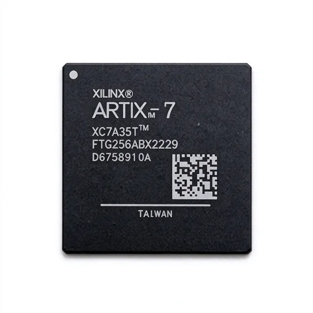
XC7A35T-2FTG256I - Artix-7 FPGA, 33K LC, 256-FTBGA | AMD Xilinx
部品番号: XC7A35T-2FTG256I ✓ 生産中| 数量 | 単価 | 小計 |
|---|---|---|
| 1 | $53.4375 | $53.44 |
| 10 | $38.5938 | $385.94 |
| 100 | $34.1406 | $3,414.06 |
| 500 | $32.6563 | $16,328.15 |
| 1,000 | $31.1719 | $31,171.90 |
XC7A35T-2FTG256I 概要
A Field Programmable Gate Array (FPGA) is a semiconductor device whose logic functionality is defined after manufacturing through a programmable interconnect of configurable logic blocks (CLBs), block RAM, DSP slices, and programmable I/O. Within the broader programmable-logic taxonomy, an FPGA sits between fixed-function ASICs (high NRE, no flexibility) and microcontrollers (sequential execution, limited parallelism). The 7-series Xilinx FPGAs span four sub-families: Spartan-6 (cost-optimized legacy), Artix-7 (lowest power, transceiver-equipped mid-range), Kintex-7 (mid-high performance), and Virtex-7 (highest performance).
Key features of the XC7A35T-2FTG256I include 33,280 logic cells distributed across approximately 5,200 6-input LUTs, 1,843,200 bits (230 KB) of block RAM organized as 50 x 36 Kb blocks, and 90 DSP48E1 slices each capable of 25 x 18-bit multiply-accumulate at up to 628 MHz. The device integrates two 10-bit ADCs (1 MSPS), four clock management tiles (CMTs) each containing one MMCM and two PLLs, and supports up to 170 user I/Os in this FTBGA-256 package.
The Artix-7 architecture delivers up to 6.6 Gb/s GTP serial transceivers and a hardened memory controller block, achieving approximately 50% lower static power and 35% lower dynamic power than the prior-generation Spartan-6 at equivalent performance. The -2 speed grade positions this part as the middle performance bin (between -1 and -3) for cost-sensitive designs that still require high DSP throughput.
Typical applications include high-volume motor control and digital signal processing front-ends, low-cost industrial Ethernet bridges, portable ultrasound and instrumentation front-ends, software-defined radio (SDR) baseband pre-processing, and machine-vision pre-processing pipelines. The combination of GTX transceivers, block RAM, and DSP48E1 slices makes the XC7A35T-2FTG256I well suited for parallel data-path designs with moderate serial connectivity.
A key design trade-off when selecting the -2 speed grade is that the LVDS, DDR memory interface rates, and GTP transceiver line rates are constrained relative to the -3 speed grade. Designers targeting the fastest possible DDR3 or GTP line rates may need to upgrade to -3, while those optimizing for cost and still passing timing closure typically stay at -2. The industrial temperature grade extends the operating envelope beyond commercial parts, suitable for factory-floor and outdoor installations.
This page aggregates distributor pricing, pin-compatible same-package alternatives, and design-oriented guidance not duplicated in the manufacturer datasheet, including thermal, signal-integrity, and pin-mux considerations for the FTBGA-256 footprint.
ドロップイン代替品: XC7A35T-2FTG256I — 同一パッケージでピン互換。PCBの作り直しが必要な異なるパッケージの部品は除外されています。
クイック比較ツール — 並列比較する代替部品を選択:
XC7A35T-1FTG256C
✓ 在庫あり
$84.2 / 個
データシートを見る →XC7A35T-2FTG256C
📋 参考代替品(カタログ未掲載)
XC7A35T-1FTG256I
📋 参考代替品(カタログ未掲載)
XC7A15T-1FTG256I
📋 参考代替品(カタログ未掲載)
XC7A35T-2FTG256E
📋 参考代替品(カタログ未掲載)
XC7A35T-2FTG256I 最大定格&電気的特性
| Family | Artix-7 |
| Logic Cells | 33,280 |
| Slices | 5,200 |
| Block RAM | 1,843,200 bits (50 x 36 Kb blocks) |
| DSP48E1 Slices | 90 |
| User I/Os (max in FTBGA-256) | 170 |
| Clock Management Tiles (CMTs) | 4 (1 MMCM + 2 PLLs each) |
| GTP Transceivers | 4 (up to 6.6 Gb/s) |
| Speed Grade | -2 |
| Temperature Grade | Industrial (-40C to +100C) |
| Process Node | 28 nm HKMG |
| パッケージ | 256-ball FTBGA (FTG256) |
| 実装タイプ | Surface Mount (BGA) |
| RoHS ステータス | Compliant |
| Lead-free | Yes |
XC7A35T-2FTG256I 256-ball ftbga (ftg256) ピン配置ガイド
XC7A35T-2FTG256I (256-ball ftbga (ftg256) パッケージ) のピン配置。 このデジタルICには、GPIO、通信インターフェース (UART、SPI、I2C)、および電源ピンが含まれています。代替ピン機能と設定オプションについては、メーカーのデータシートを参照してください。組み込みシステム設計とPCBレイアウトに不可欠です。

詳細なピン配置データはありません: XC7A35T-2FTG256I.
詳細は データシート をご参照ください。
主な用途
XC7A35T-2FTG256I の用途: 6 件s: Industrial Motor Control and Drive Front-End, Software-Defined Radio (SDR) Baseband Pre-Processing, Portable Medical Imaging Front-End, Machine Vision Pre-Processing Pipeline, Low-Cost Industrial Ethernet Bridge / Protocol Converter, Avionics / UAV Payload Data Routing.
Industrial Motor Control and Drive Front-End
The XC7A35T-2FTG256I is well matched for industrial motor control and drive front-end processing because its 90 DSP48E1 slices deliver approximately 90 GMACs of arithmetic throughput, which directly enables multi-axis Field-Oriented Control (FOC) loops with field-weakening, sensorless estimation, and PWM generation within microsecond update rates. The 1,843,200-bit block RAM (50 x 36 Kb blocks) holds extended lookup tables for sine/cosine, Park/Clarke, and SVM modulation without leaking to external memory. The -2 speed grade and industrial -40C to +100C junction rating suit factory-floor cabinet environments without derating. The 28 nm HKMG process keeps static power low enough that convection-cooled designs are viable for lower duty cycles. The GTP transceivers can drive industrial Ethernet protocols (EtherCAT, PROFINET) on the same silicon, reducing BOM. Place decoupling and ground pinout guidance per AMD UG475 for noise immunity.
おすすめ
Software-Defined Radio (SDR) Baseband Pre-Processing
The XC7A35T-2FTG256I is widely adopted as a SDR baseband pre-processing engine thanks to its combination of DSP48E1 slices, GTX-class GTP transceivers up to 6.6 Gb/s, and 1,843 Kb of on-chip block RAM. The DSP48E1 chain implements digital down-conversion (DDC), FIR filtering, channelization, and FFT cores at hundreds of MSPS, while block RAM provides data buffering between sample-rate conversion stages without external memory contention. The GTP lanes accept high-speed ADC samples or carry digitized IF between the FPGA and a host processor. The 28 nm HKMG process keeps power low enough for portable/handheld SDR radios. The -40C to +100C industrial temp grade supports outdoor and vehicular deployments. Use the FTG256 ball map to identify MGTAVCC/MGTAVTT and GTP lane pairs and follow the AMD transceiver PCB layout guidelines.
おすすめ
Portable Medical Imaging Front-End
The XC7A35T-2FTG256I is well suited for portable medical imaging front-ends (handheld ultrasound, point-of-care diagnostics) because its 90 DSP48E1 slices execute parallel beamforming, Hilbert transforms, and envelope detection at sample rates compatible with multi-channel transducer arrays. The 1,843 Kb block RAM holds entire scan-line sample buffers, avoiding power-hungry external memory accesses during image acquisition. The -2 speed grade supports 25 x 18-bit MACs at up to 628 MHz per the Artix-7 datasheet, satisfying real-time beamforming deadlines. The 28 nm HKMG process delivers low static power for battery-operated designs. The industrial -40C to +100C temperature grade suits EMS vehicles and outdoor clinics. Compliance considerations (IEC 60601, isolation barriers) are external to the silicon and must be addressed in the surrounding analog chain and PCB layout.
おすすめ
Machine Vision Pre-Processing Pipeline
The XC7A35T-2FTG256I accelerates machine-vision pre-processing (filtering, edge detection, FFT-based pattern matching) using its 90 DSP48E1 slices and 170 user I/Os from the FTG256 package. The 1,843 Kb block RAM holds line buffers for multi-megapixel sensors without external DRAM, reducing latency and BOM. GTP transceivers handle MIPI-CSI2 or parallel camera serialization to a host SoC. The -2 speed grade and -40C to +100C junction span factory-floor deployments. AMD Xilinx Vivado IP catalog provides pre-validated Vision Libraries and Image Signal Processing (ISP) cores that map efficiently onto this device. Designers must respect DDR-style PCB layout rules for high-speed parallel sensor LVDS interfaces routed through the FTBGA-256 inner-row balls.
おすすめ
Low-Cost Industrial Ethernet Bridge / Protocol Converter
The XC7A35T-2FTG256I is a strong fit for industrial Ethernet bridges and protocol converters (e.g., EtherCAT, PROFINET, Modbus TCP, EtherNet/IP) because of its four integrated GTP transceivers supporting GbE-class line rates, sufficient DSP slice count for protocol stack acceleration, and small block RAM for packet buffering. The 28 nm HKMG process enables fanless deployments on factory floors with -40C to +100C industrial temperature ratings. The FTBGA-256 footprint provides ample user I/Os for parallel fieldbus bridges and QSPI memory expansion. AMD provides industrial Ethernet IP cores that target the Artix-7 resource budget of this part. Use the FTG256 ball map to confirm MGTREFCLK0/1 routing, and follow AMD's PCB design guidelines for the MGT supply filtering network.
おすすめ
Avionics / UAV Payload Data Routing
The XC7A35T-2FTG256I is adopted in UAV and small-aviation payload systems because the Artix-7 family provides exceptional logic density per watt, and the -2 speed grade suffices for sRIO, SpaceWire, and custom avionic bus interfaces implemented on the 90 DSP48E1 slices. The industrial -40C to +100C temperature rating plus low-power 28 nm HKMG static and dynamic characteristics support extended flight times with battery or solar power. The four GTP transceivers are used for camera-link, multi-gigabit sensor aggregation, or satellite modem connectivity at up to 6.6 Gb/s. The FTBGA-256 package is compatible with constrained-area SWaP-C UAV payloads. Validate MIL-STD-810 shock/vibration profiles externally; the silicon's only electrical qualification is the industrial temperature range.
おすすめ
おすすめ製品の概要
エンジニアリング参考データ: XC7A35T-2FTG256I — 比較、設計ガイダンス、コンプライアンス情報。
選定ガイド
代替品との比較
| パラメータ | この製品 | XC7A35T-2FTG256C | XC7A35T-1FTG256C | XC7A35T-1FTG256I | XC7A15T-1FTG256I | XC7A35T-2FTG256E |
|---|---|---|---|---|---|---|
| Package | FTBGA-256 (FTG256) | FTBGA-256 (FTG256) - same | FTBGA-256 (FTG256) - same | FTBGA-256 (FTG256) - same | FTBGA-256 (FTG256) - same | FTBGA-256 (FTG256) - same |
| Brand | AMD | AMD | AMD | AMD | AMD | AMD |
| Speed Grade | -2 | -2 | -1 | -1 | -1 | -2 |
| Temperature Grade | Industrial (-40C to +100C) | Commercial (0C to +85C) | Commercial (0C to +85C) | Industrial (-40C to +100C) | Industrial (-40C to +100C) | Extended (-40C to +125C) |
| Logic Cells | 33,280 | 33,280 | 33,280 | 33,280 | 16,640 | 33,280 |
| Block RAM (Kb) | 1,800 | 1,800 | 1,800 | 1,800 | 900 | 1,800 |
| DSP48E1 Slices | 90 | 90 | 90 | 90 | 45 | 90 |
| GTP Transceivers | 4 | 4 | 4 | 4 | 4 | 4 |
主な差別化要因
- Wider industrial temperature range than the C-suffix parts (vs XC7A35T-2FTG256C)
- Higher speed grade Fmax than -1 alternatives (vs XC7A35T-1FTG256I)
- Twice the logic and DSP resources vs smaller XC7A15T parts (vs XC7A15T-1FTG256I)
設計ノート
Estimated: The Artix-7 FPGA at 90% utilization in the FTBGA-256 package dissipates between 1.5W and 3.0W. AMD's published theta-JA for this package is approximately 14 C/W on a JEDEC 4-layer test PCB, so worst-case junction rise is 3.0W x 14 C/W = 42 C above ambient. For industrial envelope with T-amb up to 85 C, junction remains below 127 C (within the 100 C industrial spec); for high-altitude or sealed enclosures, add a thermal pad copper pour under the package center balls and consider PCB-stack-up copper balancing per UG475.
Use the AMD Artix-7 package pinout files (UG475) to derive the FTBGA-256 land pattern; ball pitch is 1.0 mm and the package is 17 x 17 mm. Place 100 nF X7R 0402/0204 decoupling caps within 2 mm of every VCCINT/VCCAUX/VCCO ball cluster. MGTAVCC (1.0 V) and MGTAVTT (1.2 V) require isolated power islands and a PI-type filter network (inductor + capacitor + bulk) per UG476 to keep GTP transceiver jitter compliant.
GTP transceiver pairs (MGTRXP/N) must be routed as 100-ohm differential with intra-pair skew below 0.7 ps and matched length within the GT group. Length-match all MGTREFCLK_P/N pairs to within +/-20 mil of the target GTP lane. Avoid vias in GT differential pairs; if unavoidable, use back-drilled vias. Use the Vivado I/O Planner to verify signoff before tape-out.
Do not assume all Artix-7 FTBGA-256 packages have identical GTP ball maps - the FTG256 footprint used here must be cross-checked against the package-pinout-files CSV per Artix-7 revision. A common pitfall is reusing a Spartan-6 or Kintex-7 PCB with the wrong MGT supply pin assignments, which leads to silent link failures. Always validate the bitstream PROM files against the silicon revision stamped on the package top.
コンプライアンス情報
RoHS and REACH compliant per AMD product documentation; extended product longevity through Xilinx FPGAs Long-term Support program for industrial markets. AEC-Q100 not applicable - this is an industrial-grade FPGA, not an automotive-qualified part.







