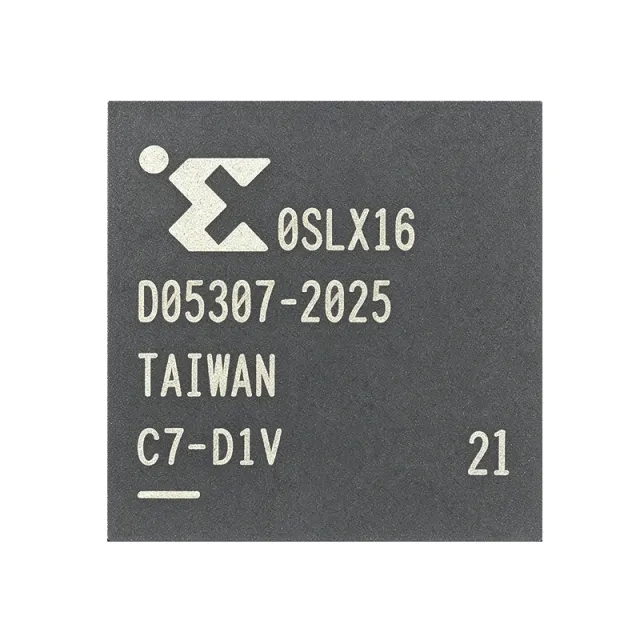
XC3S50A-4TQ144I
XC3S50A-4TQ144I - 50K Spartan-3A FPGA | AMD/Xilinx
The AMD/Xilinx XC3S50A-4TQ144I is a Spartan-3A field-programmable gate array with 50,000 system gates, 1,584 configurable logic cells, 55,296 RAM bits, and 108 I/O in a 144-LQFP package. It operates from a 1.14 V to 1.26 V core supply and is specified for an industrial junction-temperature range of -40°C to 100°C. The -4 suffix identifies the device speed grade, while the TQ144 package designation identifies the surface-mount 144-lead package used by the XC3S50A family.
A field-programmable gate array, or FPGA, is a semiconductor whose digital logic, interconnect, and I/O behavior can be programmed after manufacture. Within the product hierarchy, an FPGA is a programmable logic device and ultimately a semiconductor. Compared with a fixed-function application-specific integrated circuit, an FPGA allows parallel hardware functions, interface adaptation, and design revisions without changing the PCB. The Spartan-3A family is positioned for compact, cost-sensitive designs requiring moderate logic density and extensive user I/O.
The Spartan-3A architecture provides five principal programmable functional elements, including configurable logic blocks, programmable interconnect, dedicated block RAM, input/output blocks, and configuration resources. Each configurable logic block contains four-input lookup tables and flip-flop resources for implementing combinational and sequential logic. The available 1,584 logic cells and 55,296 RAM bits support control logic, bus arbitration, low-speed communication interfaces, instrumentation, and general-purpose digital processing.
With 108 I/O, the XC3S50A-4TQ144I offers more interface capacity than the smallest devices in the Spartan-3A family. The 144-LQFP package exposes those I/O along with configuration and power pins on a conventional surface-mount footprint. The 50,000-gate rating describes the family’s system-gate scale rather than a guaranteed clock rate, while the -4 speed designation and the manufacturer’s timing specifications determine actual performance. Configuration and pinout details should be verified against the DS529 family datasheet before PCB release.
Typical applications include industrial control, telecommunications equipment, consumer electronics, embedded instrumentation, interface bridging, and low-density signal-processing systems. In each case, the combination of 1,584 logic cells, 55,296 RAM bits, 108 I/O, and a compact 144-lead package allows logic and interface functions to be consolidated without adopting a larger FPGA or a separate microcontroller for basic control tasks.
Designers should preserve the required core-supply decoupling, use the manufacturer-recommended configuration interface, and confirm every signal’s I/O standard, drive strength, slew rate, and termination requirements against the DS529 datasheet. Programming tools, bitstream compatibility, and end-of-life considerations should also be reviewed because FPGA toolchains and family support evolve over time.
This page consolidates verified distributor availability, package and resource details, drop-in replacement analysis, and practical design guidance into a compact engineering reference. It distinguishes documented device facts from parameters that still require manufacturer-data or board-level confirmation.
견적 요청
문의하기