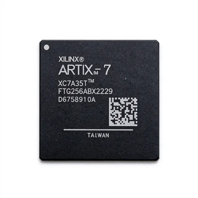
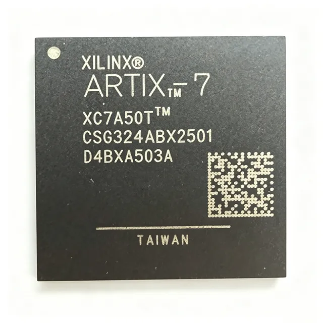
XC7A75T-1FGG676C
XC7A75T-1FGG676C - 75,520-Cell Artix-7 FPGA | AMD
AMD XC7A75T-1FGG676C is an Artix-7 field-programmable gate array with 75,520 programmable logic cells, 300 I/O, a 1 V supply range, and a 676-ball FBGA package. It is built on 28 nm CMOS technology and targets designs requiring dense programmable logic, high-speed digital processing, and flexible I/O without the cost and complexity of a larger FPGA family. The -1 designation identifies the device speed grade, while FGG676 identifies its 676-ball fine-pitch BGA package.
An FPGA is a programmable digital semiconductor whose configurable logic blocks, routing fabric, block RAM, DSP resources, and I/O can be adapted to a wide range of digital functions. Within the semiconductor hierarchy, the XC7A75T is an Artix-7 FPGA, combining programmable logic, programmable I/O, embedded memory, DSP processing, clock management, and high-speed serial transceiver resources. This integration allows control, data acquisition, signal processing, and communication functions to be implemented in one device.
Key features include 75,520 logic cells, 300 I/O, a 0.95 V to 1.05 V operating-voltage range, and operation up to 85 °C. The Artix-7 architecture uses 28 nm CMOS technology and supports clocking resources including MMCM and PLL blocks. Its combination of logic density, memory, DSP capability, and I/O availability makes it useful for industrial controls, test equipment, embedded processing, communications, and signal-processing systems.
The device provides programmable logic blocks connected by an adaptive routing network, along with dedicated block RAM, DSP slices, clock-management resources, and high-speed I/O. The verified part data identifies a maximum clock frequency of 1098 MHz, although practical interface timing depends on the selected I/O standard, clock topology, speed grade, board implementation, and external components. Configuration, power sequencing, clocking, and decoupling must follow AMD guidance for the selected Artix-7 package.
Typical applications include industrial automation controllers, programmable measurement systems, embedded video and image-processing pipelines, communication gateways, and digital signal-processing platforms. The 300 available I/O support interfaces to external converters, memory, transceivers, and control logic, while 75,520 logic cells provide substantial parallel-processing capacity. The integrated DSP and memory resources can accelerate filtering, waveform generation, and data-shaping functions.
Designers should allocate the FBGA676 footprint and its ball grid carefully, provide stable power rails and high-quality decoupling, and follow the official Artix-7 package-pinout and PCB-design guidance. Clock inputs and high-speed interfaces require controlled impedance routing. Because FPGA routing and configuration affect timing closure, the final design must be validated with the appropriate AMD Vivado tools, device files, and timing constraints.
This page consolidates verified device attributes, distributor sourcing information, strict same-package drop-in alternatives, application guidance, and design cautions. It also distinguishes exact ordering-code changes from true pin-compatible replacements so engineers can migrate a 676-ball Artix-7 design without overlooking speed grade or temperature-range differences.
견적 요청
문의하기