제품 (39,000+)

JHL9580 - Thunderbolt 5 Dual Port Host Controller | Intel
JHL9580

JHL9580 - Thunderbolt 5 Dual Port Host Controller | Intel

The Intel JHL9580 (formerly Barlow Ridge) is a Thunderbolt 5 dual-port host controller designed for desktop add-in cards, mobile platforms, and high-end docking stations. It implements Thunderbolt 5 on a PCIe 4.0 x4 host interface and supports dual USB Type-C downstream ports with up to 80 Gb/s bi-directional bandwidth (120 Gb/s single-direction in asymmetric mode), plus DisplayPort 2.1 with 8K@60Hz passthrough and USB PD 3.1 charging up to 100 W per port. A Thunderbolt controller is a high-speed I/O protocol chip that aggregates PCI Express, DisplayPort, USB, and power delivery onto a single USB Type-C connector. Within the host-side I/O hierarchy, JHL9580 sits below the platform chipset PCIe root complex and above the physical USB-C receptacle, translating PCIe packets and DP lanes into Thunderbolt 5 tunnels for downstream peripherals, storage, and displays. Key features include PCIe 4.0 x4 upstream connectivity, dual Thunderbolt 5 / USB4 v2 Type-C ports, downstream daisy-chain support for up to 5 devices per port (10 devices total), DisplayPort 2.1 with UHBR20 link training, and USB PD 3.1 EPR signaling. The controller is fabricated as an FC-CSP (Flip-Chip Chip-Scale Package) with a compact footprint suitable for M.2 add-in cards and half-length PCIe boards. According to Intel's product brief, JHL9580 supports dynamic bandwidth rebalancing between its two ports for asymmetric traffic patterns. Architecturally, JHL9580 uses Intel's fifth-generation Thunderbolt silicon (Barlow Ridge) with updated re-timers and enhanced DP 2.1 muxing. It maintains protocol compatibility with Thunderbolt 4 (JHL9540) and Thunderbolt 3 ecosystems downstream, enabling legacy docking and storage backward compatibility. The PCIe 4.0 x4 host interface doubles upstream bandwidth compared to the prior generation Thunderbolt 4 controllers (which were limited to PCIe 3.0 x4). Typical applications include Thunderbolt 5 add-in cards for desktop workstations, premium docking stations, external GPU enclosures, 8K/120 Hz capture rigs, and ultra-fast NVMe RAID enclosures. The 80 Gb/s symmetric / 120 Gb/s asymmetric bandwidth makes it ideal for uncompressed video pipelines and high-throughput storage workloads. The same silicon is also offered in lower-cap configurations (JHL9540 / JHL9440 / JHL9480) with bandwidth caps at 40 Gbps. When designing with JHL9580, ensure the platform provides a PCIe 4.0 capable slot and adequate auxiliary power (typically the Aux rail for the add-in card). Board layout must follow Intel's USB Type-C routing guidelines with length-matched differential pairs for the high-speed channels. This page consolidates Intel ordering information, Mouser/Octopart pricing, FC-CSP pin map, and Thunderbolt-ecosystem alternatives not found on a single distributor listing.

견적 요청 문의하기
JHL9580-S-RN7W - Thunderbolt 5 Dual Port Host Controller | Intel
JHL9580-S-RN7W

JHL9580-S-RN7W - Thunderbolt 5 Dual Port Host Controller | Intel

The Intel JHL9580-S-RN7W is a Thunderbolt 5 host controller (Dual Port Host configuration) implemented as an FC-CSP (Flip-Chip Chip-Scale Package) IC and shipped in tray packaging. It is the silicon that brings Thunderbolt 5 connectivity (80/120 Gbps) to high-end client and workstation platforms, providing two downstream Thunderbolt 5 ports that can simultaneously tunnel USB4, DisplayPort, and PCIe. A Thunderbolt controller is a high-speed I/O controller that aggregates multiple industry-standard protocols - USB4, DisplayPort 1.4a/2.1, and PCIe - onto a single reversible USB-C physical connector. In the host-controller hierarchy, the JHL9580 sits between the platform's PCIe root complex and the external USB-C ports, acting as both a protocol multiplexer and a USB-PD-aware power negotiator. It is paired with a discrete companion retimer on longer cable runs. Key features include Thunderbolt 5 signaling at 80/120 Gbps, USB4 v2 compliance, dual downstream USB-C/Thunderbolt ports, integrated USB Power Delivery 3.1 negotiation, and DisplayPort 2.1 alt-mode support. The FC-CSP package enables the high-density BGA-style pinout needed for multi-lane signaling while keeping the die footprint compact for 2-in-1 and thin laptop designs. Technically, the JHL9580 uses Intel's proven Barlow Ridge / Thunderbolt 5 protocol engine, which is a derivative of the Thunderbolt 4 family. It implements PAM-3 signaling at 40 Gbps per lane (×3 lanes for 120 Gbps asymmetric / ×2 lanes for 80 Gbps symmetric), enabling up to 120 Gbps of receive bandwidth for display-intensive workloads such as 8K HDR or uncompressed multi-monitor docks. Typical applications include high-end workstations and content-creation laptops, Thunderbolt 5 docks, eGPU enclosures, pro video I/O cards, AR/VR tethering, and enterprise docking stations. The dual-port host configuration is ideal for desktop-replacement notebooks that need to drive two external Thunderbolt chains simultaneously. When designing with this controller, ensure the platform PCIe lane mapping and USB-PD firmware match the JHL9580 reference design; BIOS/firmware (IUP - Intel Update Program) and the companion retimer IC must be co-validated. Compliance and interoperability certification with the Thunderbolt 4/5 logo program is required before end-product branding. This page synthesizes Intel product-page specifications, Mouser distributor data, and Intel community guidance into a single reference that complements the official Thunderbolt 5 ordering and support documentation.

견적 요청 문의하기
JHL9580-S-RN7X - Thunderbolt 5 Dual-Port Host Controller | Intel
JHL9580-S-RN7X

JHL9580-S-RN7X - Thunderbolt 5 Dual-Port Host Controller | Intel

The Intel JHL9580-S-RN7X is a Thunderbolt 5 dual-port host controller housed in an FC-CSP (Foundry Chip-Scale Package) and shipped in Tape & Reel packaging. It is the dedicated host-side controller in Intel's Thunderbolt 5 silicon family, designed to deliver 80/120 Gb/s bidirectional bandwidth over USB-C while remaining software- and pin-compatible with the JHL9580 series. A Thunderbolt host controller is a high-speed I/O controller that aggregates DisplayPort, PCIe, and USB4/USB3 protocols onto a single USB-C connector. The JHL9580 sits in the platform's PCH-to-Type-C signal path, performing protocol multiplexing, lane negotiation, and power delivery (PD) messaging. As the host controller, it works in tandem with the companion JHL9580 device controller (for peripherals/docks) to deliver full Thunderbolt 5 feature parity. Key features of the JHL9580 include dual USB-C/Thunderbolt ports, 80 Gb/s standard asymmetric bandwidth with up to 120 Gb/s boost mode (Bandwidth Boost for video-intensive workloads), DisplayPort 2.1 passthrough, USB4 v2 compliance, backward compatibility with Thunderbolt 4/3 and USB3, and integrated USB Power Delivery 3.1 support. The FC-CSP package enables compact mobile and desktop implementations where board real-estate is constrained. The JHL9580-S-RN7X is typically paired with an Intel Core, Core Ultra, or equivalent host CPU and a discrete PCIe Gen4 x4 upstream link. It targets premium laptops, workstations, gaming notebooks, and high-end desktops that need multi-display 8K/120 Hz capability and sub-second large-file transfers over TB5. Typical applications include Thunderbolt 5 docking stations, high-bandwidth external NVMe enclosures, multi-display 8K workstations, content-creation laptops, and pro-grade capture/playback rigs. Per Intel, connectivity and throughput depend on OEM implementation. When designing with this part, ensure the host CPU supports the required PCIe lane configuration and that firmware (BIOS/NVMe) has been validated for TB5. Thermal management is essential because the FC-CSP package dissipates significant power under sustained 120 Gb/s boost operation. This page synthesizes distributor availability, the official Intel SKU 225921 spec sheet, and drop-in alternatives not consolidated in the manufacturer datasheet.

견적 요청 문의하기
JMB575 - SATA 6Gb/s 5-Port Multiplier Chip | JMicron
JMB575

JMB575 - SATA 6Gb/s 5-Port Multiplier Chip | JMicron

The JMicron JMB575 is a single-chip SATA 6Gb/s Port Multiplier / Port Selector controller integrating six high-speed Serial I/O blocks, six independent SATA upper layers, an embedded microprocessor, SRAM, and PROM in a 64-pin QFN package. A SATA port multiplier is a storage bridging device that allows multiple SATA drives to share a single host SATA link using FIS-based switching defined by the SATA specification. Within the storage-IC hierarchy (interface controller -> SATA bridge -> storage controller), the JMB575 sits between one host SATA 6Gb/s port and up to five device ports, arbitrating traffic without host software changes. Key features include 1-to-5-port Port Multiplier mode, 5-to-1-port Port Selector mode, SATA 6Gb/s (SATA III) line rates on all six serial channels, and fully embedded firmware - the chip boots from internal PROM and SRAM with no external flash required. An external flash interface is available for custom firmware when extended capability is needed. Architecturally, the JMB575 combines six serial I/O macrocells with six SATA protocol engines and an on-chip microprocessor that runs JMicron's embedded firmware. Cascaded mode allows multiple JMB575 devices to be chained, connecting up to 15 drives to a single host port - useful in multi-bay enclosures where each cascade level shares the 6Gb/s host bandwidth. Typical applications include multi-bay DAS (direct-attached storage) enclosures, NAS backplane expansion behind a 6-port SATA host controller such as ASMedia ASM1166, external USB-to-5x-SATA adapters (commonly paired with the JMS580 USB-to-SATA bridge), and industrial storage subsystems. Design consideration: because all cascaded drives share one 6Gb/s host link, sustained aggregate throughput per drive decreases with cascade depth - plan bandwidth budgets accordingly and verify drive spin-up stagger settings for power sequencing in multi-bay products. This page synthesizes distributor data, JMicron product documentation, and practical deployment notes (cascading, USB pairing) not found in the two-page product brief.

견적 요청 문의하기
JMB582 - PCIe Gen3x1 to 2-Port SATA 6Gb/s Bridge | JMicron
JMB582

JMB582 - PCIe Gen3x1 to 2-Port SATA 6Gb/s Bridge | JMicron

The JMicron JMB582 is a PCIe Gen3 x1 to dual-port SATA 6Gb/s bridge controller that connects a PCI Express host to two SATA storage devices, provided in a 48-pin QFN (6x6 mm) surface-mount package. It integrates JMicron self-designed PCIe and SATA PHYs in a single chip and supports SATA Revision 3.2, AHCI, NCQ, TRIM, hot plug, and port multiplier operation. A PCIe-to-SATA bridge controller is an interface IC that translates between the PCI Express host bus protocol and the Serial ATA (SATA/AHCI) device protocol. In the storage-signal-chain hierarchy it sits between the host PCIe root port and SATA SSD/HDD endpoints, allowing motherboards, embedded x86 platforms, IPC, and servers to expand the number of SATA ports without changing the host chipset. Key features include a PCIe Gen3 x1 upstream port (compatible with PCIe 3.1a and backward compatible with PCIe 2.0/1.x), two independent SATA 6Gb/s host ports, support for both AHCI and legacy IDE programming interfaces, NCQ (Native Command Queuing), TRIM pass-through to SSDs, and PCIe link-layer power-saving modes for low idle power. The integrated PHYs eliminate external PHY chips, reducing BOM cost and board area. Architecturally, the JMB582 uses JMicron in-house PCI Express and SATA PHY macrocells with a packet-based protocol bridge. The upstream link nearly saturates the PCIe Gen3 x1 line bandwidth (approximately 985 MB/s usable), which is sufficient to drive two SATA 6Gb/s devices (up to about 550 MB/s each) in typical workloads. Port multiplier support allows additional drives per SATA port where required. Typical applications include M.2-to-SATA and PCIe-to-SATA add-in cards (such as the Seeed ODYSSEY-X86J4105 expansion and Waveshare dual M.2 SATA expander), NAS/home-server storage expansion, industrial PCs and consumer electronics requiring extra SATA connectivity. Design-wise, place the 3.3V input decoupling close to the QFN power pins, route the PCIe and SATA differential pairs with 100-ohm controlled impedance, and confirm the host BIOS exposes AHCI mode for TRIM support. This page adds value beyond the JMicron datasheet by synthesizing distributor availability, orderable variant cross-references (JMB582-QHCA0A, JMB582-QHCB0A), design notes, and application guidance in one place.

견적 요청 문의하기
JMB585 - PCIe Gen3x2 to 5-Port SATA 6Gb/s Bridge | JMicron
JMB585

JMB585 - PCIe Gen3x2 to 5-Port SATA 6Gb/s Bridge | JMicron

The JMicron JMB585 is a PCIe Gen3 x2 to 5-port SATA 6Gb/s bridge controller in a QFN-76 package, providing five SATA III (AHCI) host ports with Port Multiplier support and near-line-rate PCIe Gen3 x2 bandwidth of up to 2 GB/s aggregate throughput. A bridge controller is a specialized interface IC that translates one bus protocol into another, sitting in the storage hierarchy between the host (PCIe root complex) and the storage device layer (SATA/AHCI drives). In a typical PC system, the JMB585 occupies the same role as a chipset-integrated SATA controller: it enumerates as a standard AHCI host, so operating systems treat its ports exactly like native motherboard SATA ports. Key features include five independent SATA 6Gb/s downstream ports, an upstream PCIe Gen3 x2 (about 2 GB/s) link, native AHCI and legacy IDE mode support, SSD TRIM command pass-through, and Port Multiplier support for expanding beyond five drives. JMicron emphasizes that the device almost fully saturates the PCIe Gen3 x2 line bandwidth, which matters when multiple SSDs are accessed concurrently. Technically, the JMB585 is highly integrated with JMicron self-designed PCI Express and SATA PHY IP on a single die, eliminating external PHY chips and reducing BOM cost and board area. Firmware operates transparently with in-box AHCI drivers in Linux, Windows, and most UEFI/BIOS implementations, which is why JMB585-based M.2 A+E and M.2 B+M adapter cards are popular in NAS and home-server builds. Typical applications include M.2-to-5xSATA expansion adapters for NAS servers (TrueNAS, Unraid), desktop storage upgrade cards, embedded x86 platforms such as the ODYSSEY-X86J4105, and industrial storage expansion where driverless AHCI compatibility is required. A key design consideration: the PCIe Gen3 x2 uplink (approx. 2 GB/s) is shared across all five SATA ports, so total concurrent bandwidth saturates at roughly two SATA SSDs running at full 6Gb/s speed; mechanical HDD workloads are never limited. This page synthesizes distributor availability, drop-in alternative analysis versus ASMedia ASM1166 and JMB582, and practical design notes not found in the manufacturer datasheet.

견적 요청 문의하기
JMS580 - USB 3.1 Gen2 to SATA 6Gb/s Bridge | JMicron
JMS580

JMS580 - USB 3.1 Gen2 to SATA 6Gb/s Bridge | JMicron

The JMicron JMS580 is a USB 3.1 Gen 2 to SATA 6Gb/s bridge controller that connects a USB host to SATA storage devices such as HDDs and SSDs. Its USB 3.1 Gen 2 upstream interface delivers data rates up to 10Gbps, double the USB 3.1 Gen 1 rate, while the downstream SATA port is fully compliant with SATA 6Gb/s specifications. A bridge controller is a protocol-conversion IC that sits between two different bus standards, translating transaction-level commands so devices on either side can communicate transparently. Within the storage semiconductor hierarchy, the JMS580 belongs to the class of USB-to-SATA bridge ICs, which are themselves part of the broader peripheral controller and storage interface IC category used across external drives, docks, and adapters. Key features include native support for the USB Attached SCSI Protocol (UASP), which substantially elevates command throughput versus legacy Bot (Bulk-Only Transport), and TRIM command pass-through for SSDs, preserving long-term NAND write performance in external enclosures. The 10Gbps USB 3.1 Gen 2 link allows fast SATA SSDs to be nearly fully utilized at the interface level, and JMicron notes the single-chip solution saves cost, PCB board space, and development time for storage device developers. Architecturally, the JMS580 integrates USB 3.1 Gen 2 PHY and link layers, a SATA 6Gb/s controller, and protocol translation firmware handling SCSI/ATA command conversion, UASP queuing, and TRIM forwarding. JMicron's peripheral portfolio spans USB 3.1 Gen 2, Gen 1, USB 2.0, and FireWire, supporting single-bay, dual-bay, and multi-bay drive products, Blu-ray/DVD players, and NAS devices with RAID capabilities. Typical applications include external USB-C/USB 3.1 hard drive and SSD enclosures, USB-to-SATA adapter cables and dongles, docking stations, and multi-bay arrays where the JMS580 is paired with the JMB575 SATA port multiplier to connect up to five drives to a single USB host. A key design consideration is that real-world throughput is bounded by the slower of the USB link and the drive's SATA interface; HDDs rarely exceed 250 MB/s, so full 10Gbps benefit is only visible with SATA SSDs. Firmware for UASP and TRIM behavior should be validated against the host OS before production. This page synthesizes distributor data, verified JMicron datasheet content, drop-in alternative candidates, and practical design notes not found in the manufacturer datasheet alone.

견적 요청 문의하기
JS28F320J3F75A - 32Mbit Parallel NOR Flash, 75ns, 56-TSOP | Micron
JS28F320J3F75A

JS28F320J3F75A - 32Mbit Parallel NOR Flash, 75ns, 56-TSOP | Micron

The Micron JS28F320J3F75A is a 32-Mbit (4M x 8 / 2M x 16) parallel NOR flash memory device with a 75 ns initial access time, operating from a 2.7 V to 3.6 V single supply, and housed in a 56-pin Thin Small Outline Package (TSOP Type I). It belongs to the J3 family of embedded flash memories built on 65 nm Single Bit per Cell (SBC) technology, providing reliable non-volatile code and data storage for embedded systems. A parallel NOR flash is a non-volatile memory type that supports random read access (execute-in-place / XIP), byte-level program, and sector erase operations. Within the memory hierarchy, NOR flash sits between SRAM (volatile, fastest) and NAND flash (non-volatile, higher density, sequential access). NOR is preferred when a microprocessor needs to fetch code directly from the array without first copying to RAM, and when reliable long-term data retention with low software complexity is required. Key features include symmetric 128-Kbyte uniform blocks (parameter blocks) or 64-Kword blocks, top or bottom boot block configurations, hardware write protection, a deep power-down mode for low standby current, and command-set compatibility with the Common Flash Interface (CFI). The device supports 100,000 program/erase cycles per block and a minimum 20-year data retention. Its 75 ns access time makes it suitable for microprocessors and ASICs operating at bus frequencies up to approximately 50 MHz without wait states, or higher with proper handshaking. Typical applications include set-top boxes, networking equipment, industrial controllers, automotive infotainment, printers, and any embedded design requiring execute-in-place boot storage. The 56-TSOP footprint is widely supported on legacy and new PCBs, simplifying hardware integration. When designing with this device, ensure the host microcontroller supplies a clean 3.3 V rail within the 2.7 V-3.6 V tolerance, and respect the program/erase timing budget. Adding a 0.1 uF decoupling capacitor close to VCC and VCCQ pins is recommended for reliable operation across temperature. This page synthesizes distributor pricing, drop-in alternatives, and practical design notes not found in the manufacturer datasheet alone. All values are referenced to current Micron datasheet and live distributor inventory as of 2026-10-05.

견적 요청 문의하기
K3K8K80BM-JGCT - Samsung LPDDR DRAM Memory IC | Samsung Electronics
K3K8K80BM-JGCT

K3K8K80BM-JGCT - Samsung LPDDR DRAM Memory IC | Samsung Electronics

The Samsung Electronics K3K8K80BM-JGCT is a mobile DRAM memory IC from Samsung's K3K series of low-power SDRAM components, supplied in a ball grid array (BGA) package for space-constrained mobile and embedded designs. Samsung's K3K part-number prefix designates its LPDDR (Low Power Double Data Rate) DRAM component family used in smartphones, tablets, and embedded computing platforms. Low-power DDR DRAM is a class of volatile memory that transfers data on both edges of the clock to double bandwidth while reducing operating and standby power. Within the memory hierarchy, LPDDR sits below DDR5 server DIMMs in raw bandwidth but dominates mobile and battery-powered systems because of its low core voltage, deep power-down modes, and PoP (Package-on-Package) or discrete BGA mounting options. It is a direct child of the broader SDRAM/DRAM semiconductor category. Key characteristics of this device class include high-speed bidirectional data transfer, per-bank and per-rank power management, dynamic voltage and frequency scaling, and initialization/training sequences defined by the JEDEC LPDDR specification in force for the die generation. Samsung mass-produces these dies on advanced DRAM process nodes with stacked or planar cell arrays. Architecturally, Samsung LPDDR components integrate the memory array, sense amplifiers, row/column decoders, DLL/phase-alignment circuitry, and I/O gating on a single die, with the package ball map exposing the CA (command/address) bus and DQ data lanes. Typical applications include smartphone application-processor memory, tablet and notebook SoC main memory, automotive infotainment memory subsystems, and embedded AI/edge-computing modules that require high bandwidth per watt. A key design consideration is signal integrity: LPDDR CA/DQ routing requires length-matched, impedance-controlled traces and careful fly-by or daisy-chain topology, and controller training must match the Samsung die's datasheet timing parameters. This page synthesizes verified distributor data, same-family alternative MPNs, and practical design notes not found in the manufacturer datasheet.

견적 요청 문의하기
K3K9K90BM-MGCP - LPDDR5 DRAM | Samsung Semiconductor
K3K9K90BM-MGCP

K3K9K90BM-MGCP - LPDDR5 DRAM | Samsung Semiconductor

The Samsung K3K9K90BM-MGCP is an LPDDR5 (Low Power Double Data Rate 5) DRAM memory integrated circuit from Samsung Semiconductor, supplied in a PBGA (Plastic Ball Grid Array) package. Samsung's LPDDR5 family delivers pin speeds of up to 6400 Mbps and aggregate bandwidth of up to 51.2 GB/s per device, with approximately 20% lower power consumption than the previous LPDDR4X generation. LPDDR5 DRAM is a type of synchronous dynamic random-access memory optimized for low power and high bandwidth in mobile, edge computing, and embedded systems. In the memory hierarchy it sits under the DRAM -> synchronous DRAM -> low-power SDRAM taxonomy defined around the JEDEC LPDDR5 standard, and it succeeds LPDDR4X in mobile SoC memory subsystems. Key features of Samsung LPDDR5 devices include 6400 Mbps pin speed, deep power-down and per-bank refresh architectures that cut idle power, and a simplified two-channel architecture that improves command efficiency versus LPDDR4X. Density options across the K3K/K3L family range from 32 Gbit to 64 Gbit per package, organized as x32-wide interfaces for SoC attachment. Technically, LPDDR5 introduces WCK (word clock) strobing, bank group architecture, and DVFS (dynamic voltage frequency scaling) of the clock domain, allowing the memory controller to throttle speed and voltage to match workload, which is the main source of the ~20% system power saving versus LPDDR4X. Typical applications include flagship smartphone and tablet main memory, AI edge accelerators, automotive infotainment and ADAS platforms, and 5G networking equipment where high bandwidth per watt is critical. Design consideration: LPDDR5 signal integrity requires tightly matched length routing of CA, DQ, DQS, and WCK traces on the PCB; consult the Samsung LPDDR5 design guide for fly-by topology and termination recommendations. This page synthesizes distributor stock data, drop-in same-family alternatives, and practical design notes not found in the manufacturer datasheet.

견적 요청 문의하기
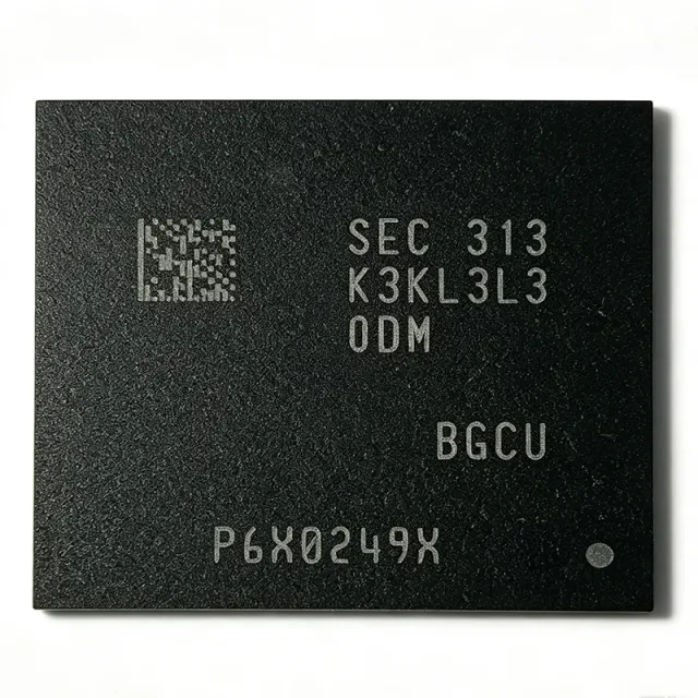
K3KL3L30DM-BGCU - LPDDR5X 64Gb 8533Mbps DRAM | Samsung
K3KL3L30DM-BGCU

K3KL3L30DM-BGCU - LPDDR5X 64Gb 8533Mbps DRAM | Samsung

The Samsung Semiconductor K3KL3L30DM-BGCU is a 64 Gb LPDDR5X low-power DRAM memory IC operating at 8533 Mbps data rate, organized x64, in a 496-ball FBGA package. It operates from multiple supply rails of 1.8 V, 1.05 V, 0.9 V and 0.5 V and is rated for -25 C to +85 C operation. LPDDR (Low Power Double Data Rate) SDRAM is a type of synchronous dynamic random-access memory optimized for mobile and power-sensitive systems. Within the memory hierarchy, LPDDR5X sits at the top of the JEDEC low-power DRAM family (LPDDR4 -> LPDDR5 -> LPDDR5X), functioning as the main-system memory IC that feeds CPUs, GPUs and NPUs in smartphones, tablets, automotive computing platforms and AI edge devices. Key features of the K3KL3L30DM-BGCU include its 8533 Mbps pin speed, which places it in the highest LPDDR5X speed bin, and its 64 Gb density per device, enabling multi-gigabyte system memory with only a few ICs. The x64 organization and 496-ball FBGA footprint allow dense PCB routing on mobile-style boards. Technically, LPDDR5X extends LPDDR5 with higher signaling rates and improved power efficiency. Samsung states its LPDDR5X family delivers up to 8.5 Gbps data processing speeds with approximately 20% better power efficiency than LPDDR5, making it suited to AI inference, high-resolution imaging pipelines and 5G data throughput. Typical applications include flagship smartphone main memory, automotive infotainment and ADAS compute modules, AI edge accelerators, and premium tablet and laptop DRAM subsystems paired with Qualcomm or MediaTek application processors. A key design consideration is power-integrity: LPDDR5X at 8533 Mbps demands tight rail regulation on the 0.5 V VDDQ domain, careful fly-by trace length matching and per-rail decoupling per the memory controller vendor layout guide. This page consolidates distributor stock signals, family cross-references and practical sourcing notes beyond the bare datasheet listing. Pricing is RFQ-based as of 2026-09-04 because this EOL-status part trades through broker channels rather than fixed catalog tiers.

USD $45.94 재고 있음
K3KL3L30QM-JGCT - LPDDR5X 64Gb 7500Mbps DRAM | Samsung
K3KL3L30QM-JGCT

K3KL3L30QM-JGCT - LPDDR5X 64Gb 7500Mbps DRAM | Samsung

The Samsung K3KL3L30QM-JGCT is a 64 Gb LPDDR5X DRAM memory IC organized x64, supporting data rates up to 7500 Mbps per pin, supplied in a fine-pitch ball grid array (FBGA) package for mobile and edge computing platforms. LPDDR5X (Low Power Double Data Rate 5X, per the JEDEC LPDDR5X standard family) is an extension of LPDDR5 that raises signaling speed and improves power efficiency for battery-operated and thermally constrained systems. In the memory hierarchy it sits as volatile main-system DRAM below persistent storage such as NAND flash and eMMC, providing the working memory bandwidth that CPUs, GPUs, and NPUs require. Key features of the K3KL3L30QM-JGCT include its 64 Gbit density (8 GB equivalent per device), x64 organization for wide memory buses, and 7500 Mbps/pin data rate, which places it in the LPDDR5X performance tier used by flagship smartphones, tablets, AI edge accelerators, and automotive infotainment SoCs. As a Samsung third-generation 10nm-class DRAM product line part, it delivers higher bandwidth than LPDDR5 at lower power per transferred bit. Technically, LPDDR5X operates with a low-voltage I/O rail (VDDQ around 0.3-0.5 V class, per Samsung LPDDR5X documentation) and uses advanced training, on-die termination, and link ECC-style features inherited from LPDDR5 to maintain signal integrity at multi-gigabit speeds. Ball-grid-array interconnects minimize parasitic inductance, enabling clean eye diagrams at 7500 Mbps when the PCB stackup follows Samsung's package-on-package and fly-by routing guidance. Typical applications include flagship smartphone and tablet main memory, AI accelerator and NPU buffer memory, automotive domain-controller DRAM, and high-performance embedded and edge-server modules such as LPDDR5X SODIMMs and memory-down designs. Design consideration: LPDDR5X signal integrity is highly layout sensitive - length-matched, reference-plane-continuous routing and strict power-integrity budgeting for VDDQ are mandatory; insufficient decoupling at 7500 Mbps manifests as training failures rather than gradual degradation. This page adds value beyond the datasheet by synthesizing distributor stock levels, drop-in family alternatives, and practical design notes in one place.

견적 요청 문의하기
K3KL5L50DM-BGCU - LPDDR5X 128Gb 8533Mbps DRAM | Samsung
K3KL5L50DM-BGCU

K3KL5L50DM-BGCU - LPDDR5X 128Gb 8533Mbps DRAM | Samsung

The Samsung Semiconductor K3KL5L50DM-BGCU is a premium low-power DRAM (LPDDR5X) memory IC offering 128 Gb (16 GB) of density and an 8533 Mbps data rate per pin, packaged in a fine-pitch ball grid array (496-ball FBGA per distributor listings). It belongs to Samsung's LPDDR5X family, which delivers up to 8.5 Gbps pin speeds and approximately 20% better power efficiency than LPDDR5 at comparable speeds. LPDDR5X (Low Power Double Data Rate 5X) is an JEDEC-defined evolutionary step of the LPDDR5 SDRAM standard, aimed at mobile, automotive, and edge-AI computing systems. In the memory hierarchy, DRAM sits as the main system memory between the processor and non-volatile storage, providing high-bandwidth working memory; LPDDR variants optimize this role for battery-powered and thermally constrained devices by lowering I/O and core voltages and adding deep power-down states. Key characteristics of this part include the 128 Gb monolithic density, the 8533 Mbps (8.5 Gbps) transfer rate per data pin, and the ultra-low-power architecture typical of Samsung's LPDDR5X portfolio, which supports dynamic voltage scaling and advanced sleep modes. The high pin speed translates directly into memory bandwidth critical for large-language-model inference, 5G modems, and high-resolution imaging pipelines. Technically, LPDDR5X devices use bank group architectures with 16n prefetch, on-die termination, and command/address training to sustain multi-gigabit signaling. Samsung's premium LPDDR5X line further emphasizes power efficiency through enhanced ECC features and refined process nodes, allowing smartphone SoCs and automotive ADAS platforms to exploit full bandwidth within tight thermal envelopes. Typical applications include flagship smartphone and tablet main memory (often stacked as multi-die packages), AI accelerator companion memory in edge servers, automotive infotainment and ADAS domains, and high-performance embedded modules. A key design consideration: LPDDR5X signal integrity at 8.5 Gbps demands strict fly-by topology routing, length-matched traces, and SoC memory-controller training support; dropping to an LPDDR5-only controller limits operation to 6400 Mbps class speeds. This page synthesizes distributor stock data (16,750 pcs reported as of Aug 31, 2026), same-family alternatives, and practical design notes not found in the manufacturer datasheet.

견적 요청 문의하기
K3KL5L50QM-JGCT - 128Gb LPDDR5X 7500Mbps DRAM | Samsung
K3KL5L50QM-JGCT

K3KL5L50QM-JGCT - 128Gb LPDDR5X 7500Mbps DRAM | Samsung

The Samsung K3KL5L50QM-JGCT is a 128 Gb (16 GB) LPDDR5X low-power DRAM memory IC delivering data rates up to 7500 Mbps per pin with a x64 organization, housed in a 441-ball FBGA package operating from -25C to +85C across 1.8 V, 1.05 V, 0.9 V and 0.5 V supply domains. LPDDR5X (Low Power Double Data Rate 5X eXtended) is an enhanced evolution of the LPDDR5 DRAM standard defined by JEDEC. As a class of volatile DRAM within the broader memory hierarchy (LPDDR5X -> LPDDR family -> DRAM -> semiconductor memory), it prioritizes bandwidth-per-watt for battery-powered and thermally constrained compute platforms. Compared with LPDDR5, LPDDR5X raises interface speed and improves power efficiency, making it the dominant main-memory technology for flagship smartphones, tablets, and increasingly for AI accelerators and automotive computing. Key features of the K3KL5L50QM-JGCT include its 128 Gb monolithic density in a compact 441-ball FBGA footprint, 7500 Mbps (LPDDR5X-7500) interface speed, x64 channel organization suitable for 16-bit channel stacking, and an industrial-extended -25C to +85C operating range. Samsung reports that its premium LPDDR5X generation delivers up to 1.25 times the speed and roughly 25% better power efficiency versus the previous generation. Technically, the device uses Samsung advanced DRAM process technology with a multi-rail power architecture: VDD1 (1.8 V), VDD2 (1.05 V), VDDQ (0.5 V) and VDDCA/other aux rails, minimizing I/O switching power at multi-gigabit rates. The x64 organization allows SoC memory controllers to aggregate two 32-bit channels for full-bandwidth LPDDR5X operation. Typical applications include flagship smartphone and tablet main memory, AI edge computing and inference accelerators, in-vehicle infotainment and ADAS compute modules, and high-performance ultra-thin PCs. Design consideration: because this part is a ball-grid array memory, signal integrity on the command/address and data buses is critical; follow the SoC vendor reference layout for fly-by routing, ODT settings, and power rail sequencing. This page synthesizes distributor stock, drop-in family alternatives, and practical design notes not found in the manufacturer datasheet.

견적 요청 문의하기
K3KL7L70EM-MGCU - 12Gb LPDDR5X DRAM, 315-Ball FBGA | Samsung
K3KL7L70EM-MGCU

K3KL7L70EM-MGCU - 12Gb LPDDR5X DRAM, 315-Ball FBGA | Samsung

The Samsung K3KL7L70EM-MGCU is a 12 Gigabit (12 Gb) LPDDR5X low-power synchronous DRAM memory chip from Samsung Semiconductor, supplied in a 315-ball FBGA (Fine-Pitch Ball Grid Array) surface-mount package. This LPDDR5X DRAM is engineered for bandwidth-intensive, power-sensitive mobile and edge-computing platforms, operating at a data rate of up to approximately 8533 Mbps/pin as offered in Samsung's LPDDR5X family. LPDDR5X (Low Power Double Data Rate 5X eXtended) is an evolution of the LPDDR5 memory standard defined by JEDEC, pushing data rates and energy efficiency beyond conventional LPDDR5. In the memory hierarchy, DRAM sits between on-chip SRAM caches and non-volatile storage such as NAND flash, serving as the main working memory of a system-on-chip (SoC). LPDDR5X specifically targets flagship smartphones, tablets, AI edge accelerators, automotive infotainment, and high-performance portable devices that need more bandwidth than LPDDR5 at comparable or lower power. Key features of the K3KL7L70EM-MGCU include its 12 Gb single-die density, LPDDR5X-class speed grading (suffix -MGCU denotes speed and package options per Samsung part numbering), the compact 315-ball FBGA footprint, and Samsung's advanced low-voltage VDDQ operation that reduces I/O power versus LPDDR5. Samsung's LPDDR5X process technology supports deep power-down, per-bank refresh, and advanced bank-group architectures that improve effective bandwidth and standby efficiency. Architecturally, the device is organized as a x32-class LPDDR5X SDRAM with bank groups supporting burst-access scheduling. Command/address and data signals use Samsung LPDDR5X signaling with on-die termination (ODT) and link error checking options implemented per JEDEC LPDDR5X conventions, simplifying SoC PHY integration for Qualcomm Snapdragon and MediaTek Dimensity class platforms. Typical applications include flagship smartphone main memory, AI inference accelerators at the edge, automotive cockpit and ADAS domain controllers, and ultra-thin tablets or laptops using stacked/package-on-package memory configurations. When designing this device in, ensure the SoC memory controller explicitly supports LPDDR5X timing and speed-bin compatibility, and follow Samsung's layout guidelines for fly-by routing of CA/CLK nets and matched-length DQ/DBI/DQS groups. This page consolidates verified distributor listings, drop-in family alternatives, and practical design guidance not found in a single manufacturer datasheet.

견적 요청 문의하기
K3KL9L90CM-MGCT - 64Gb LPDDR5X 7500Mbps x32 DRAM | Samsung
K3KL9L90CM-MGCT

K3KL9L90CM-MGCT - 64Gb LPDDR5X 7500Mbps x32 DRAM | Samsung

The Samsung K3KL9L90CM-MGCT is a 64 Gbit LPDDR5X SDRAM with a x32 memory organization and a maximum data rate of 7500 Mbps, housed in a 315-ball FBGA (BGA-315) package. LPDDR5X (Low Power Double Data Rate 5X) is an enhanced evolution of the LPDDR5 standard defined by JEDEC, targeting dramatically higher bandwidth with lower operating voltage. It sits at the top of the mobile DRAM hierarchy (LPDDR4X -> LPDDR5 -> LPDDR5X) and serves as the main-system-memory technology for smartphones, tablets, laptops, AI accelerators, and automotive infotainment platforms. As volatile memory, it provides fast working storage for a processor but must be re-initialized at every power cycle. Key features of this device include the 64 Gbit density per die (8 GByte per package in x32 organization), 7500 Mbps pin speed for approximately 300 Gbps of aggregate bandwidth per 32-bit channel, and LPDDR5X-class low supply voltages (VDDQ 500 mV core interface domain with 900 mV/1.05 V core rails and 1.8 V I/O and power domains per the JLCPCB listing). The industrial-grade operating range of -25C to +85C supports demanding embedded deployments. Architecturally, the device implements LPDDR5X signaling with dynamic voltage scaling, deep sleep modes, and per-bank refresh schemes inherited from LPDDR5, enabling platforms compliant with JEDEC JESD209-5B-class requirements to exploit full 7500 Mbps operation. Command/address training and DFE-based receiver equalization sustain signal integrity at high data rates over standard PCB stackups. Typical applications include AI edge-compute modules, high-performance smartphone and tablet main memory, industrial controllers requiring embedded logging, computing/COM express modules, and firmware boot and data-storage subsystems that pair DRAM with NAND. Design consideration: LPDDR5X at 7500 Mbps requires strict fly-by termination topology, length-matched routing, and careful power-domain isolation of the 500 mV VDDQ rail; memory-controller training quality directly determines achievable speed bin. This page consolidates verified distributor stock, drop-in same-family alternatives, and practical sourcing guidance not found in the manufacturer datasheet.

견적 요청 문의하기
K3LKBKB0BM-MGCP - 32Gbit LPDDR5 DRAM 6400Mbps | Samsung
K3LKBKB0BM-MGCP

K3LKBKB0BM-MGCP - 32Gbit LPDDR5 DRAM 6400Mbps | Samsung

The Samsung K3LKBKB0BM-MGCP is a 32 Gbit LPDDR5 SDRAM memory IC with a 1G x32 organization and a data rate of 6400 Mbps, operating from 500 mV, 900 mV, 1.05 V and 1.8 V supply rails over an industrial-extended temperature range of -25C to +85C. The device is packaged in a fine-pitch FBGA ball grid array (data indicates FBGA-315, 1.05 V core class) and is RoHS compliant. LPDDR5 (Low Power Double Data Rate 5) is the fifth generation of JEDEC low-power synchronous DRAM, a class of volatile memory that stores working data for application processors and SoCs. Within the memory hierarchy, LPDDR5 sits under the broader DRAM family alongside DDR4/DDR5, but is optimized for bandwidth-per-watt in battery-powered and thermally constrained systems rather than raw module capacity. Key differentiating specifications include the 6400 Mbps/pin data rate, which doubles effective LPDDR4X-class bandwidth in comparable channel conditions; a 32 Gbit single-die density that allows 4 GB of memory in one package with a x32 I/O interface; and multi-rail operation (VDD1 1.05 V class core, VDD2 0.9 V class, VDDQ 0.5 V class, VDD2H 1.8 V class per the distributor listing) that reduces dynamic and standby power. The -25C to +85C operating window extends beyond the standard mobile range, supporting industrial controllers and outdoor connected devices. Technically, the device belongs to Samsung's LPDDR5 family, which uses deep-sleep states, bank-group architecture, and dynamic voltage frequency scaling to cut idle power dramatically versus LPDDR4. Speed-class grading (this part is listed alongside LPDDR5-5500/6400 class material in web listings) allows platform designers to match memory bandwidth to SoC controller capability. Signal integrity at 6400 Mbps requires careful length-matched routing and reference-plane discipline on the PCB. Typical applications include flagship smartphones and tablets, AI edge-compute modules, automotive infotainment SoCs, networking appliances, and industrial computing modules where 4 GB LPDDR5 density and low standby power are required. Design consideration: at 6400 Mbps, routing and power-delivery design dominate system margins; use fly-by topology guidance from the Samsung LPDDR5 datasheet and validate the design at the corner data rates during SI/PI sign-off. This page synthesizes distributor pricing, stock availability, drop-in alternative guidance, and practical design notes not found in the manufacturer datasheet alone.

USD $46.62 문의하기
K3LKCKC0BM-MGCP - 64Gb LPDDR5 6400Mbps DRAM | Samsung
K3LKCKC0BM-MGCP

K3LKCKC0BM-MGCP - 64Gb LPDDR5 6400Mbps DRAM | Samsung

The Samsung Semiconductor K3LKCKC0BM-MGCP is a 64 Gb LPDDR5 SDRAM DRAM with a 6400 Mbps data rate, organized as 2G x32, housed in a 315-ball FBGA (PBGA315) package. It operates from multiple supply rails (500 mV, 900 mV, 1.05 V, 1.8 V) across an industrial-grade -25 C to +85 C temperature range, and is RoHS compliant. LPDDR5 (Low Power Double Data Rate 5) is a JEDEC-defined generation of mobile DRAM optimized for high bandwidth and low power consumption in battery-operated and performance-driven systems. Within the memory hierarchy, DRAM is a volatile random-access memory used as main system memory, sitting between the processor and non-volatile storage such as NAND flash. LPDDR5 succeeds LPDDR4X with higher data rates, lower operating voltage, and power-saving features. Key features of the K3LKCKC0BM-MGCP include its 64 Gbit density (8 GB per die), the LPDDR5 parallel interface running at 6400 Mbps per pin, and a 32-bit-wide memory organization (2G x32). These attributes make it well suited to flagship smartphone SoCs, AI edge accelerators, and automotive infotainment platforms that demand high memory bandwidth with tight power budgets. Technically, the device uses CMOS technology in a fine-pitch ball grid array, with core, I/O, and interface rails split across 500 mV/900 mV/1.05 V/1.8 V domains per LPDDR5 power architecture. The FBGA-315 ball map supports high-speed signal routing with controlled impedance and on-die termination practices defined by the LPDDR5 specification. Typical applications include mobile handset main memory, AI/edge computing modules, 5G networking equipment buffers, and automotive infotainment and ADAS compute platforms. Design consideration: strict length-matched PCB routing and reference-plane integrity are essential at 6400 Mbps; follow the Samsung datasheet layout guidelines for ball mapping, decoupling, and VDDQ rail design. This page synthesizes distributor pricing, stock availability, drop-in family alternatives, and practical design notes not found in the manufacturer datasheet.

견적 요청 문의하기
K4A4G045WD-BCPB - 4Gb DDR4 SDRAM x4 1.2V | Samsung
K4A4G045WD-BCPB

K4A4G045WD-BCPB - 4Gb DDR4 SDRAM x4 1.2V | Samsung

The Samsung K4A4G045WD-BCPB is a 4Gb (1G x 4) DDR4 SDRAM from Samsung's D-die family, operating at 1.2V with a DDR4-2133 (PC2133) speed bin, housed in a 78-ball TFBGA (FBGA) surface-mount package. DDR4 SDRAM (Double Data Rate 4 Synchronous Dynamic Random Access Memory) is the fourth generation of the JEDEC-defined DDR memory hierarchy, following DDR, DDR2, and DDR3. Within the memory IC taxonomy it sits under DRAM -> SDRAM -> DDR SDRAM -> DDR4 SDRAM. DDR4 devices transfer data on both clock edges, doubling effective bandwidth per clock, and introduce lower operating voltage (1.2V vs 1.5V for DDR3), bank groups, and improved on-die termination for higher data rates and lower power in computing systems. Key features of the K4A4G045WD include 4Gb density organized as 1G x 4 (per Samsung and distributor data DDR4 1Gx4 PC2133), 1.2V core supply, DDR4-2133 speed class, and the compact 78-ball TFBGA package that enables dense memory subsystem layouts. The D-die process generation offers mature yield and long-lifecycle production status within Samsung's DDR4 portfolio. Architecturally, the device uses DDR4 bank-group organization with internal prefetch and standard DDR4 command interface (ACT, READ, WRITE, REF, PRE), supporting burst lengths of 8 with sequential and interleaved options, per the Samsung DDR4 SDRAM datasheet Rev. 1.1 (66 pages) covering the K4A4G045WD and K4A4G085WD family. Typical applications include desktop and notebook PC DIMM and soldered-down memory, networking and communication equipment, industrial controllers, and server-adjacent subsystems requiring stable long-term supply. A key design consideration: DDR4 signal integrity requires careful length-matched routing, VTT termination, and controller-calibrated write leveling; verify the memory controller supports the DDR4-2133 timing set (speed bin defined in CL-tRCD-tRP order per Samsung). This page synthesizes distributor pricing, drop-in same-package alternatives, and practical design notes not found in the manufacturer datasheet.

견적 요청 문의하기
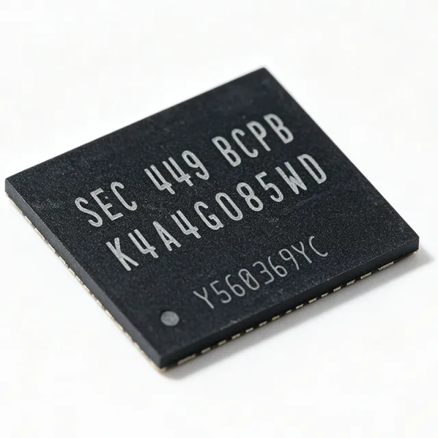
K4A4G085WD - 4Gb DDR4 SDRAM 512Mx8 BGA | Samsung
K4A4G085WD

K4A4G085WD - 4Gb DDR4 SDRAM 512Mx8 BGA | Samsung

The Samsung K4A4G085WD is a 4Gb (512M x 8) DDR4 SDRAM in the D-die generation, fabricated on Samsung's advanced DRAM process and delivered in a 78-ball FBGA package. It operates from a 1.2V core supply at data rates up to DDR4-2400 with typical CAS latency settings of CL15 to CL17, depending on speed grade suffix. A DDR4 SDRAM (Double Data Rate 4 Synchronous Dynamic Random Access Memory) is a type of volatile DRAM that transfers data on both clock edges, doubling effective bandwidth versus SDR memory. Within the memory hierarchy it sits as the main-system-memory tier: DRAM cell -> DDR SDRAM -> DDR4 SDRAM -> memory IC -> semiconductor memory. DDR4 introduced the bank-group architecture, lower 1.2V operation, and improved on-die termination (ODT) relative to DDR3. Key features of the K4A4G085WD include the 8-bit-wide x8 I/O organization with 512M addressable locations, the DDR4 bank-group architecture that accelerates random access by permitting interleaved access to different bank groups, and low 1.2V power operation that cuts power consumption versus DDR3. Built-in termination and the CA parity option improve signal integrity at high bus speeds on long, heavily loaded memory buses. The D-die core uses Samsung's scaled DRAM cell technology, supporting standard DDR4 timing parameters such as tRCD, tRP and tRAS per the JEDEC DDR4 specification framework and the Samsung product guide. The 78-ball FBGA (Fine-Pitch Ball Grid Array, lead-free solder balls) keeps the footprint compact for dense memory subsystems, and the part is available in commercial speed grades such as -BCPB (DDR4-2400) and -BCRC, as identified in the Samsung DDR4 SDRAM Memory product guide (May 2018). Typical applications include embedded controllers, industrial computing modules, networking equipment, set-top boxes, and replacement/repair sourcing for PC DIMMs and UDIMM/SODIMM assemblies using x8 DRAM components. When designing with this device, follow Samsung's layout guidance for fly-by command/address routing, per-byte DQS strobe matching, and 40-ohm ODT calibration; address-bus integrity at DDR4-2400 is the most common failure point in first-turn boards. This page synthesizes verified datasheet data, drop-in alternatives across Samsung, Micron and SK Hynix families, practical design notes, and procurement information not found in the manufacturer datasheet alone.

USD $2.05 문의하기
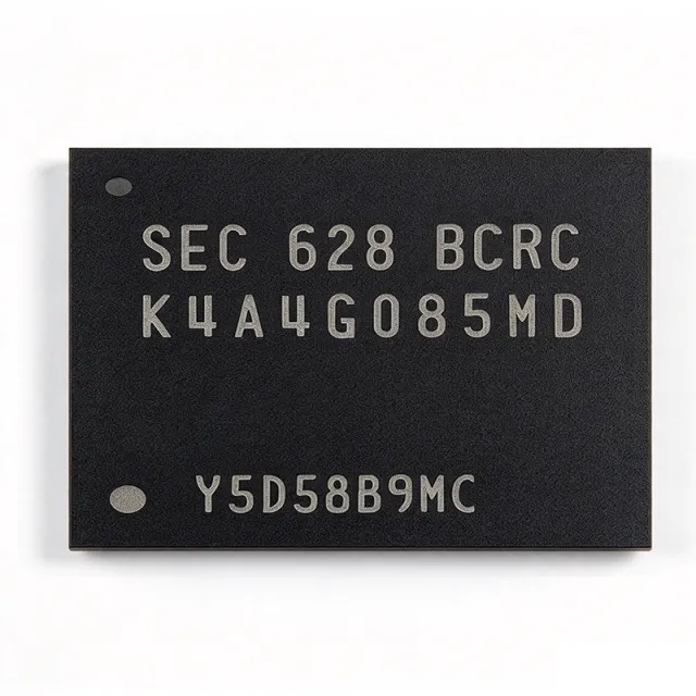
K4A4G085WD-BCRC - 4Gb DDR4-2400 SDRAM 512Mx8 | Samsung
K4A4G085WD-BCRC

K4A4G085WD-BCRC - 4Gb DDR4-2400 SDRAM 512Mx8 | Samsung

The Samsung K4A4G085WD-BCRC is a 4Gb DDR4 SDRAM organized as 512M x 8, operating at a data rate of 2400 Mb/s (PC2400) with a 1.2V core supply, housed in a 78-ball FBGA (TFBGA) package. DDR4 SDRAM (Double Data Rate 4 Synchronous Dynamic Random Access Memory) is a type of volatile memory that transfers data on both the rising and falling edges of the clock signal, doubling effective bandwidth compared to SDR memory. Within the memory hierarchy, DRAM sits below CPU caches and above storage devices such as NAND flash, serving as the primary working memory in computing systems. The JEDEC-standardized DDR4 generation operates at 1.2V, down from DDR3's 1.5V, reducing system power while raising transfer rates. Key features of the K4A4G085WD-BCRC include the 4Gb D-die configuration from Samsung's DDR4 family, a x8 data interface suitable for controllers with narrower memory buses, and the space-saving 78-ball fine-pitch BGA footprint that supports high-density memory subsystems on compact PCBs. Samsung continues to lead the industry with one of the broadest DRAM portfolios, and this device is found in applications from embedded controllers to computing modules. Technically, the device uses a multi-bank page burst access architecture. As a DDR4 component, it runs from a single 1.2V supply rail, requiring a memory controller that implements DDR4 initialization, training, and refresh scheduling. The x8 organization means a 64-bit system bus is typically populated with eight devices per rank; single-device designs can use the x8 data mask functionality available in DDR4 x8 parts. Typical applications include industrial controllers, embedded computing modules, network appliances, firmware execution and data logging buffers, and replacement sourcing for DDR3-era designs migrating to the DDR4 platform. Design consideration: verify that your memory controller supports DDR4-2400 speed bin timing and that the power delivery network supplies a clean 1.2V rail with proper VTT termination, since signal integrity at 2400 Mb/s on fly-by routed address/command buses demands careful length matching and ODT tuning. This page synthesizes distributor pricing, drop-in alternatives, and practical design notes not found in the manufacturer datasheet.

견적 요청 문의하기
K4A4G085WD-BCRC - 4Gb DDR4-2400 SDRAM 512Mx8 | Samsung
K4A4G085WD-BCRC

K4A4G085WD-BCRC - 4Gb DDR4-2400 SDRAM 512Mx8 | Samsung

The Samsung K4A4G085WD-BCRC is a 4Gb DDR4 SDRAM organized as 512M x 8 bits, operating at DDR4-2400 (PC4-2400) data rates from a 1.2V supply, housed in a 78-ball FBGA package. It belongs to Samsung's D-die DDR4 generation. DDR4 SDRAM is the fourth generation of Double Data Rate synchronous dynamic random-access memory, a class of volatile memory ICs that transfer data on both clock edges. Within the memory hierarchy, DDR4 sits above DDR3 and below DDR5, and is the dominant DRAM technology for embedded controllers, industrial modules, and enterprise computing platforms. Compared to DDR3, DDR4 lowers the core supply from 1.5V to 1.2V, raises bank-group parallelism, and improves bus speeds. Key features of the K4A4G085WD-BCRC include the 4Gbit density in a byte-wide x8 organization, DDR4-2400 speed grade (BCRC speed bin), and 1.2V low-voltage operation that reduces system power versus DDR3. The device supports standard DDR4 features such as bank-group architecture, on-die termination (ODT), and DBI/CRC functionality typical of the DDR4 specification. Technically, the D-die Samsung DDR4 family uses a scaled DRAM process with bank groups enabling higher effective bandwidth. The x8 organization suits designs using a single chip per data lane, simplifying layout for microcontroller FMC/SDRAM-style controllers and industrial compute modules that need moderate bandwidth and non-standard memory sizing. Typical applications include industrial controllers and PLCs requiring DRAM working memory, embedded computing and networking modules, firmware logging and data buffering systems, and replacement sourcing for legacy DDR4-based BOM lines. Distributors such as Jotrin, Censtry, and Weyland list the part as DDR4 512Mx8 PC2400. Design consideration: DDR4 demands careful signal-integrity work - length-matched fly-by routing of CK/CA/DQS, accurate VTT termination on the 1.2V bus, and controller configuration of tRFC and ZQ calibration. Verify the exact speed bin suffix (BCRC) against your controller's supported rates. This page synthesizes distributor pricing, drop-in alternatives across Samsung die generations and a JEDEC-compatible Micron equivalent, plus practical DDR4 design notes not found in the manufacturer datasheet.

USD $4.10 재고 있음
K4A8G085WB-BCPB - 8Gb DDR4 SDRAM 3200Mbps | Samsung
K4A8G085WB-BCPB

K4A8G085WB-BCPB - 8Gb DDR4 SDRAM 3200Mbps | Samsung

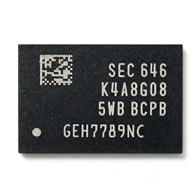
The Samsung K4A8G085WB-BCPB is an 8Gb DDR4 SDRAM memory chip organized as 1G x 8, operating at 1.2V with a data rate of 3200 Mbps (PC4-25600) in a 78-ball FBGA package. DDR4 SDRAM (Double Data Rate 4 Synchronous Dynamic Random Access Memory) is a volatile memory technology that transfers data on both rising and falling edges of the clock, doubling the effective data rate. Within the memory hierarchy it sits below the memory controller and above storage, serving as main system memory. DDR4 succeeded DDR3 by lowering the core supply from 1.5V to 1.2V (up to 40% power reduction), increasing bank count from 8 to 16 via bank groups, and raising densities to 8Gb and beyond. Key features of the K4A8G085WB-BCPB include the 3200 Mbps data rate (BC speed grade), CAS Latency 22, burst length 8, and 16 banks in 4 bank groups for improved parallelism. On-die termination (ODT) and dynamic ODT improve signal integrity, while temperature-compensated self-refresh (TCSR) reduces standby power. The device is fabricated on Samsung's advanced DRAM process (B-die generation) and supports programmable read latency (RL) and write latency (WL). It runs from a 1.2V supply (nominal) with refresh intervals of 7.8 us up to 85C operating temperature. DLL-enabled mode operation ensures precise output timing across the speed range. Typical applications include desktop and laptop DIMMs, embedded computing boards, industrial PCs, networking equipment, and test instrumentation requiring high bandwidth in a compact footprint. When designing in this component, match memory controller timing parameters (CL22 at 3200 Mbps), place decoupling capacitors close to the power balls, and follow the length-matched fly-by routing of DDR4 for CK/CA/DQS nets. This page adds distributor pricing data, drop-in alternatives within the same Samsung DDR4 x8 family, and cross-brand equivalents (SK Hynix, Micron, Nanya) not found in the manufacturer datasheet alone.

USD $13.78 재고 있음
K4A8G085WB-BCRC - 8Gb DDR4 SDRAM 1Gx8 2400Mbps | Samsung
K4A8G085WB-BCRC

K4A8G085WB-BCRC - 8Gb DDR4 SDRAM 1Gx8 2400Mbps | Samsung

The Samsung K4A8G085WB-BCRC is a high-performance 8Gb DDR4 SDRAM organized as 1G x 8, operating at 1.2V with a data rate of 2400 Mbps (PC4-19200). It is housed in a 78-ball FBGA package, designed for a wide range of computing and embedded applications requiring high bandwidth and low power consumption. DDR4 SDRAM (Double Data Rate 4 Synchronous Dynamic Random-Access Memory) is a type of volatile memory that transfers data on both edges of the clock signal, doubling the data rate compared to DDR3. It operates at a lower voltage (1.2V) than DDR3 (1.5V), reducing power consumption by approximately 25%. DDR4 is the industry standard for modern servers, desktops, laptops, and high-performance embedded systems, offering higher density and speed than its predecessors. Key features of the K4A8G085WB-BCRC include a density of 8Gb, organization of 1G x 8, and a speed grade of 2400 Mbps. It supports a temperature range of 0°C to 85°C, making it suitable for commercial applications. The device uses a 78-ball FBGA package, which provides excellent thermal and electrical performance. It also features on-die termination (ODT), programmable read/write latency, and auto-refresh and self-refresh modes for power saving. Technically, the K4A8G085WB-BCRC is built on Samsung's advanced B-die process technology, which is known for its high speed and low latency. It supports a burst length of 8 and 4, and includes a built-in temperature sensor for thermal management. The device is designed to meet JEDEC DDR4 standards, ensuring compatibility with a wide range of memory controllers. Typical applications include high-performance computing, servers, networking equipment, and industrial embedded systems. Its high density and speed make it ideal for memory-intensive tasks such as data analytics, virtualization, and real-time processing. The low operating voltage also makes it suitable for power-sensitive designs. When designing with this component, ensure proper signal integrity by following the layout guidelines in the datasheet, including controlled impedance traces and proper decoupling. The device requires a 1.2V VDD and 2.5V VPP supply, and supports a data mask for byte-wise write operations.

견적 요청 문의하기