제품 (39,000+)

KAD2708C-27Q68 - 8-Bit 275MSPS ADC LVCMOS QFN-68 | Renesas
KAD2708C-27Q68

KAD2708C-27Q68 - 8-Bit 275MSPS ADC LVCMOS QFN-68 | Renesas

The Renesas KAD2708C-27Q68 is an 8-bit, 275 MSPS, single-channel pipelined analog-to-digital converter housed in a 68-pin QFN package with an exposed thermal paddle. It is built on Intersil's proprietary FemtoCharge technology on a standard CMOS process, delivering 49.2 dBFS SNR at a 138 MHz input frequency while consuming less than 265 mW. The ADC features an over-range indicator, a selectable divide-by-2 input clock divider, and LVCMOS-compatible outputs that interface easily with FPGAs and digital ASICs. An analog-to-digital converter (ADC) is a data-conversion component that transforms a continuous-time, continuous-amplitude analog signal into discrete digital codes for downstream processing. Pipeline ADCs such as the KAD2708C are the workhorse of high-speed, moderate-resolution conversion (8-14 bits) and sit within the broader class of Nyquist-rate data converters used in instrumentation, communications, and imaging. Power management ICs, clock generators, and high-speed signal-conditioning amplifiers complete the typical signal-chain surrounding such an ADC. Key features include 49.2 dBFS SNR at 138 MHz input, 60 dBFS SFDR, less than 265 mW power dissipation at 275 MSPS, a 1.5 Vpp differential analog input range, and on-chip track-and-hold. The QFN-68 (10x10 mm) exposed-paddle package provides a low thermal resistance path, making the part suitable for thermally constrained designs without an external heatsink. Programmable full-scale range and selectable clock-divider simplify board-level clocking and gain calibration. Architecturally, the KAD2708C uses a multi-stage pipelined converter core with digital error correction, achieving 8-bit linearity without complex calibration. The FemtoCharge switched-capacitor front end samples input bandwidths well above 200 MHz, while proprietary reference-biasing schemes minimize distortion. The divide-by-2 input allows designers to feed a 550 MHz external clock and divide internally, easing clock-tree routing on dense multi-ADC boards. Typical applications include medical imaging, radar signal processing, instrumentation and oscilloscope front ends, communications receivers, and high-speed data acquisition in industrial nondestructive testing. The 275 MSPS sample rate exceeds the Nyquist requirement for many IF-band signals found in radar and software-defined radio. When designing with this ADC, ensure the analog input is AC-coupled or DC-biased within the KAD2708C common-mode range to avoid saturating the front-end switched-capacitor network. Place the analog and digital decoupling capacitors as close to the package as possible to preserve SNR and SFDR at high input frequencies. This page synthesizes distributor pricing, pin-compatible same-family alternatives, and practical layout notes not found in the manufacturer datasheet, helping engineers shorten design cycles and select drop-in replacements with confidence.

견적 요청 문의하기
KAD2708L-17Q68 - 8-bit 170MSPS ADC LVDS Output | Renesas
KAD2708L-17Q68

KAD2708L-17Q68 - 8-bit 170MSPS ADC LVDS Output | Renesas

The Renesas KAD2708L-17Q68 is a member of the pin-compatible KAD2708L family of low-power, high-performance 8-bit Analog-to-Digital Converters, specified at 170 MSPS sample rate with LVDS-compatible digital outputs, fabricated on Intersil's proprietary FemtoCharge technology node in a standard CMOS process and housed in a 68-lead RoHS-compliant QFN (10x10 mm) package with exposed thermal paddle. An analog-to-digital converter (ADC) is a mixed-signal integrated circuit that samples continuous-time analog input voltages and converts them into discrete digital codes at a defined sample rate. The KAD2708L family belongs to the pipelined ADC architecture class, a sub-category of Nyquist-rate data converters optimized for high sampling rates (>100 MSPS) with low latency and moderate resolution (8-10 bits). Pipelined ADCs sit hierarchically between SAR ADCs (lower speed, higher resolution) and flash ADCs (highest speed, lowest resolution), making them the workhorse for digitizing IF and baseband signals in communications, instrumentation, and defense systems. Key features of the KAD2708L-17Q68 include 8-bit resolution, 170 MSPS sample rate in the -17 speed grade, 1.5 Vp-p differential analog input range, 600 MHz analog input bandwidth, an on-chip voltage reference, internal track-and-hold, an over-range indicator, and a selectable divide-by-2 input clock divider. Typical dynamic performance reaches 48.8 dBFS SNR at fIN = 175 MHz, while total power consumption is held below 330 mW. Designers select this part when the system requires moderate-resolution high-speed sampling for waveform digitization, radar IF, or test equipment where LVDS signaling provides robust noise immunity over longer PCB traces and backplane interconnects. The exposed paddle aids thermal dissipation and must be soldered to a ground plane for specified performance. Typical applications include digital oscilloscopes, communications test equipment, radar/sonar IF digitizers, and high-speed data acquisition systems. When designing with this part, ensure the exposed paddle is soldered to a continuous ground plane with multiple thermal vias, the analog and digital supply domains are decoupled with 0.1 uF and 10 uF capacitors placed close to the supply pins, and LVDS traces are length-matched within the receiver skew budget.

견적 요청 문의하기
KAD2708L-21Q68 - 8-bit 210MSPS LVCMOS ADC, 68-QFN | Renesas
KAD2708L-21Q68

KAD2708L-21Q68 - 8-bit 210MSPS LVCMOS ADC, 68-QFN | Renesas

The Renesas (formerly Intersil) KAD2708L-21Q68 is a single-channel, 8-bit, 210 MSPS analog-to-digital converter built on Intersil's proprietary FemtoCharge™ technology on a standard CMOS process, offered in a 68-lead QFN (10x10 mm) package. The KAD2708L-21Q68 variant of the KAD2708L family delivers 210 MSPS sampling rate with LVCMOS digital outputs, 48.8 dBFS SNR at fIN = 175 MHz, and power consumption below 330 mW from a 1.8 V AVDD2 / 3.3 V AVDD3 supply rail. A pipelined ADC is a high-speed sampling architecture that converts an analog input through a cascade of low-resolution flash stages, each stage producing a residue passed to the next. Pipelined ADCs sit within the broader ADC hierarchy as the dominant solution for sampling rates from ~10 MSPS to ~1 GSPS where successive-approximation (SAR) converters become too slow and flash converters become impractical due to comparator count. The KAD2708L family is one of the industry's lowest-power 8-bit high-performance ADC families, designed for communications, oscilloscope, and imaging front-ends. Key features of the KAD2708L-21Q68 include 8-bit resolution, 210 MSPS maximum sampling rate, single-channel LVCMOS output, an over-range indicator for out-of-range detection, a selectable divide-by-2 input clock divider for flexible clocking, and pin compatibility across the broader KAD2708L/KAD2710C 68-QFN family offering 8- and 10-bit resolutions at 105 to 350 MSPS. The device operates from AVDD2 = 1.8 V and AVDD3 = 3.3 V supplies, providing easy interfacing to modern FPGA and ASIC LVCMOS receivers. From an architecture standpoint, FemtoCharge™ technology uses a small switched-capacitor charge-redistribution front-end combined with a pipelined core to achieve wide input bandwidth and low aperture jitter. The LVCMOS output drivers ease board-level integration with FPGAs and ASICs that do not support LVDS, removing the need for external level-translation buffers. The 68-QFN package exposes the die pad for thermal dissipation, and the part consumes under 330 mW in operation. Typical applications include digital oscilloscopes, communication test equipment, radar and lidar front-ends, IF signal digitisation in software-defined radio, medical imaging subsystems, and high-speed data-acquisition cards. The combination of low power, small footprint, and pin-compatible family scalability makes the KAD2708L-21Q68 a strong fit where multiple sampling rates or resolutions are needed across product variants. When designing with this part, ensure the analog input network is designed for the ADC's full-power input bandwidth and that the LVCMOS outputs are properly terminated at the receiver. The selectable divide-by-2 input clock divider allows use of an external clock oscillator up to 420 MHz while presenting a clean 210 MHz internal sampling clock. Decoupling must follow the datasheet reference layout, particularly the exposed pad connection to the analog ground plane. This page synthesizes distributor pricing, drop-in same-package alternatives, comparison parameters, and practical design notes not aggregated on the manufacturer datasheet, providing a single reference for sourcing, selection, and PCB-level integration decisions.

견적 요청 문의하기
KAD2708L-27Q68 - 8-Bit 275MSPS ADC LVCMOS QFN-68 | Renesas
KAD2708L-27Q68

KAD2708L-27Q68 - 8-Bit 275MSPS ADC LVCMOS QFN-68 | Renesas

The Renesas (formerly Intersil) KAD2708L-27Q68 is a low-power 8-bit, 275 MSPS single-channel analog-to-digital converter housed in a 68-lead QFN package with exposed thermal pad. It is part of the pin-compatible KAD2708L/KAD2710L family, with the -27 speed grade delivering 275 MSPS sampling while other family members reach up to 350 MSPS. Key headline parameters are 8-bit resolution, 275 MSPS maximum sample rate, LVCMOS-compatible outputs, and a 1.5 VPP differential full-scale analog input range. An ADC (analog-to-digital converter) is a data-conversion integrated circuit that translates continuous-time analog signals into discrete digital codes at a rate set by its sampling clock. High-speed pipeline ADCs such as the KAD2708L sit at the top of the data-converter taxonomy: ADC -> pipeline ADC -> high-speed ADC -> data converter IC -> mixed-signal semiconductor. They are used wherever wideband analog signals must be digitized for downstream DSP, FPGA, or ASIC processing. Differentiating specifications include 48.8 dBFS SNR at fIN = 175 MHz, 600 MHz full-power analog input bandwidth, less than 330 mW power consumption at full sample rate, an internal track-and-hold, on-chip reference, and a selectable divide-by-2 clock input. The FemtoCharge™ switched-capacitor architecture enables the low-power figure while preserving dynamic performance in the second Nyquist zone. The device uses a 1.5 VPP differential analog input, LVCMOS digital outputs, and an LVDS-style clock input (LVDS/LVCMOS compatible). It also features an over-range indicator and configurable CMOS output timing, simplifying board-level FPGA capture. RoHS-compliant 68-QFN packaging with exposed paddle keeps the die-to-ambient thermal resistance low for sustained high-speed operation. Typical applications include radar intermediate-frequency (IF) digitizers, broadband test-and-measurement equipment, communications receiver IF chains, and high-speed medical imaging front ends. The combination of 8-bit resolution, 275 MSPS sampling, and low power suits cost-sensitive yet performance-demanding designs. When designing with this part, keep analog input traces length-matched for 50 Ohm differential impedance, place the exposed paddle over a continuous ground pour, and decouple AVDD and DRVDD separately to limit digital switching noise coupling back into the analog front end. This page synthesizes distributor pricing, same-family drop-in alternatives (KAD2708L-35Q68, KAD2708L-21Q68, KAD2708L-10Q68), and practical design notes not aggregated in the manufacturer datasheet.

견적 요청 문의하기
KAD2708L-35Q68 - 8-bit, 350MSPS Single-Channel ADC | Renesas
KAD2708L-35Q68

KAD2708L-35Q68 - 8-bit, 350MSPS Single-Channel ADC | Renesas

The Renesas (formerly Intersil) KAD2708L-35Q68 is a 8-bit, 350 MSPS single-channel Analog-to-Digital Converter (ADC) with LVCMOS outputs, fabricated on Intersil's proprietary FemtoCharge technology on a standard CMOS process. It is packaged in a 68-lead QFN (10 mm × 10 mm) with an exposed thermal paddle, and it operates over -40 °C to +85 °C. This -35 speed grade is the fastest member of the KAD2708L pin-compatible family, which also includes 275/210/170/105 MSPS grades, allowing board reuse across a wide range of sampling-rate requirements. Typical dynamic performance is 48.8 dBFS SNR at fIN = 175 MHz, while total power consumption is less than 330 mW. A pipelined ADC (or pipelined analog-to-digital converter) is a multi-stage converter that cascades several low-resolution flash stages with interstage sample-and-hold and digital error correction. Pipelined ADCs are widely used in communications, instrumentation, and defense applications because they achieve sampling rates from tens to hundreds of MSPS while preserving excellent dynamic range. Within the broader taxonomy, this places the KAD2708L-35Q68 inside the data-converter family, itself a sub-domain of mixed-signal integrated circuits and ultimately the broader semiconductor category. Key features include an on-chip voltage reference, internal track-and-hold, 1.5 VP-P differential input voltage range, 600 MHz analog input bandwidth, two's-complement output format, an over-range indicator, and a selectable divide-by-2 input clock divider. The LVCMOS interface simplifies FPGA or ASIC capture without requiring an LVDS receiver, lowering BOM cost in cost-sensitive designs. Internal bandgap trimming and FemtoCharge switched-capacitor front-end design yield the low 330 mW dissipation figure, important for densely populated boards and thermally constrained enclosures. Architecture highlights include an internal track-and-hold amplifier, a 1.5 VP-P differential analog input stage, and on-chip reference. Two's-complement digital output coding is supplied through parallel LVCMOS ports with over-range flagging. The selectable divide-by-2 clock input simplifies clock-tree design by accepting a 700 MHz LVCMOS/CMOS clock and producing an internal 350 MHz sample clock, eliminating the need for an external divider. Typical applications include high-speed data acquisition, radar/EW receivers, medical imaging front-ends, communications test equipment, and set-top box / cable-modem downstream capture. Its 8-bit resolution and 350 MSPS throughput make it suitable for digitizing wide-bandwidth IF signals in software-defined-radio (SDR) receivers. Design consideration: route the analog input traces as a 100 Ω differential pair, keep AVDD2 (1.8 V) and AVDD3 (3.3 V) supplies decoupled with 0.1 µF and 10 µF ceramics close to each pin, and provide a solid thermal land pattern under the exposed paddle for heat removal. When evaluating alternatives, note that the KAD2708L family shares pinout across all speed grades, so a 27 or 17 grade can be fitted without PCB rework. This page synthesizes distributor pricing, pin-compatible drop-in alternatives drawn from the same datasheet family, and practical layout guidance - information not consolidated on the manufacturer datasheet or any single distributor listing.

견적 요청 문의하기
KAD2710C-10Q68 - 10-Bit 105MSPS Pipelined ADC | Renesas
KAD2710C-10Q68

KAD2710C-10Q68 - 10-Bit 105MSPS Pipelined ADC | Renesas

The Renesas (formerly Intersil) KAD2710C-10Q68 is a 10-bit, 105 MSPS, single-channel pipelined Analog-to-Digital Converter built on Intersil's proprietary FemtoCharge technology, packaged in a 68-pin QFN (10x10 mm) with exposed thermal paddle. The KAD2710C-10Q68 is the lowest-speed member of the KAD2710C family, offering selectable sample rates of 105/170/210/275 MSPS across the family while the -10Q68 suffix specifically denotes the 105 MSPS speed grade with LVCMOS-compatible digital outputs. A pipelined ADC is a type of analog-to-digital converter that uses cascaded low-resolution stages (typically 1.5-bit sub-ADCs and DACs with residue amplification) to digitize an analog input at high sample rates while maintaining low power consumption. Within the broader data converter hierarchy, the KAD2710C-10Q68 sits between successive-approximation (SAR) ADCs (low speed, low latency) and flash ADCs (highest speed, lowest resolution per stage), making it ideal for intermediate-frequency sampling in communications systems, portable imaging, and industrial digitizers. Key features of the KAD2710C-10Q68 include 55.6 dBFS SNR at fIN = 138 MHz, less than 265 mW power consumption at full sample rate, an over-range indicator for signal monitoring, and a user-selectable divide-by-2 input clock divider for flexible clock tree design. The CMOS process FemtoCharge architecture minimizes aperture jitter and allows the converter to maintain dynamic performance over the full industrial temperature range without active thermal management. This 10-bit ADC is designed for high dynamic performance in bandwidth-limited intermediate-frequency signal chains. The single 1:1 pipelined core with digital error correction provides spurious-free dynamic range suitable for cellular base-station receiver IF stages, digital oscilloscope front ends, and radar signal processing. The exposed paddle of the 68-QFN package provides a low thermal resistance path that supports full 105 MSPS operation across the -40 C to +85 C industrial range. Typical applications include IF sampling in wireless infrastructure, portable ultrasound beamformers, digital oscilloscope input channels, and radar return digitizers. The LVCMOS outputs interface directly with low-cost FPGAs or ASICs without requiring an external LVDS receiver, which simplifies the digital capture path for cost-sensitive designs. When designing with this ADC, ensure the analog input is bandwidth-limited to less than half the sampling rate to satisfy the Nyquist criterion. Decouple AVDD and DVDD separately with low-ESR 0.1 uF and 10 uF capacitors placed within a few millimetres of the supply pins, and provide a clean, low-jitter clock to the CLK+ / CLK- inputs for optimum SNR performance. This page synthesizes manufacturer datasheet excerpts, distributor stock and pricing, drop-in pin-compatible same-family alternatives, and practical PCB layout notes that are not collated on any single manufacturer or distributor page.

견적 요청 문의하기
KAD2710C-17Q68 - 10-Bit 170MSPS Pipelined ADC, 68-QFN | Renesas
KAD2710C-17Q68

KAD2710C-17Q68 - 10-Bit 170MSPS Pipelined ADC, 68-QFN | Renesas

The Renesas KAD2710C-17Q68 is a 10-bit, 170 MSPS, single-channel pipelined analog-to-digital converter in a 68-lead QFN (10x10 mm) exposed-pad package. It is the 170 MSPS speed grade of the KAD2710C family, which also offers 105, 210 and 275 MSPS variants, and the -17Q68 part number designates the LVCMOS-compatible output variant in the QFN-68 package. A pipelined ADC (analog-to-digital converter) is a high-speed data converter architecture that resolves an analog input through multiple cascaded low-resolution stages, each driving a residue into the next. Compared with successive-approximation or flash converters, pipelined ADCs deliver the best balance of sampling rate, resolution, power dissipation, and input bandwidth, which is why they dominate communications infrastructure, instrumentation, and imaging. The KAD2710C family is the industry's lowest-power 10-bit pipelined ADC at 275 MSPS, consuming under 265 mW with 55.6 dBFS SNR at fIN = 138 MHz, built on Renesas' proprietary FemtoCharge technology in a standard CMOS process. The KAD2710C-17Q68 integrates a selectable divide-by-2 input clock buffer, an over-range indicator for gain ranging, and an internal reference. Its LVCMOS outputs interface directly with FPGAs and ASICs at speeds up to 170 MSPS, while the exposed-paddle QFN-68 package provides low thermal resistance (theta-JA of approximately 24 C/W) suitable for industrial-temperature operation from -40C to +85C. The 1.8 V analog and 3.3 V output supply domains simplify interfacing with modern FPGA I/O without level translators. Typical applications include digital oscilloscopes, communication test equipment, IF sampling in software-defined radio, radar signal processing, medical imaging front-ends, and high-speed data acquisition cards. The 170 MSPS sampling rate easily covers intermediate-frequency bands up to 70 MHz while leaving headroom for input-bandwidth-limited anti-alias filtering. Designers should ensure the exposed paddle is soldered to a continuous ground plane and that the analog input is AC-coupled with 50 ohm-controlled impedance to realize the published ENOB and SFDR performance.

견적 요청 문의하기
KAD2710C-21Q68 - 10-Bit 210MSPS ADC | Intersil (Renesas) | QFN-68
KAD2710C-21Q68

KAD2710C-21Q68 - 10-Bit 210MSPS ADC | Intersil (Renesas) | QFN-68

The Renesas (formerly Intersil) KAD2710C-21Q68 is a 10-bit, 210 MSPS, single-channel, high-performance analog-to-digital converter (ADC) in a 68-pin QFN (10x10 mm) package with an exposed thermal pad. It belongs to the KAD2710C pin-compatible ADC family, which offers 8- and 10-bit resolutions and sample rates from 105 to 350 MSPS. The KAD2710C-21Q68 variant is the 210 MSPS speed grade with LVCMOS-compatible digital outputs. An analog-to-digital converter (ADC) is a mixed-signal integrated circuit that converts continuous analog input voltages into discrete digital codes at a specified sampling rate. High-speed ADCs like the KAD2710C sit between the analog front-end (amplifiers, filters, mixers) and the digital back-end (FPGA, ASIC, DSP) in signal acquisition systems. They are the critical bridge that determines the dynamic range, bandwidth, and fidelity of any digital receiver, oscilloscope, or radar processing chain. ADC performance is commonly characterized by SNR (signal-to-noise ratio), SFDR (spurious-free dynamic range), ENOB (effective number of bits), and aperture jitter. The KAD2710C-21Q68 leverages Intersil's proprietary FemtoCharge™ technology on a standard CMOS process to achieve 55.6 dBFS SNR at an input frequency of 138 MHz while consuming less than 265 mW. Key features include an integrated over-range indicator, a selectable divide-by-2 input clock buffer, an internal reference, and LVCMOS output drivers. The 68-pin QFN package provides an exposed paddle for low thermal resistance, allowing operation across the industrial temperature range of -40°C to +85°C. Architecture is a pipelined multi-stage ADC with on-chip sample-and-hold and internal bandgap reference, supporting single-ended analog inputs. The pipelined architecture delivers high sample rates at moderate power consumption compared to flash or successive-approximation designs. Typical applications include digital oscilloscopes, IF sampling in communications receivers, radar signal processing, medical imaging front-ends, and high-speed data acquisition cards. The wide input bandwidth supports undersampling architectures for IF digitization. When designing with this device, ensure the analog input is properly terminated and that the input clock has low jitter (< 1 ps RMS) to preserve SNR at high input frequencies. Decouple all supply pins with 0.1 µF and 10 µF capacitors placed as close to the package as possible, and tie the exposed paddle to a clean ground plane. This page synthesizes distributor pricing, drop-in same-family and cross-brand ADC alternatives, application notes, and practical PCB design guidance not collected in the manufacturer datasheet.

견적 요청 문의하기
KAD2710C-27Q68 - 10-Bit 275MSPS ADC, 68-QFN | Renesas/Intersil
KAD2710C-27Q68

KAD2710C-27Q68 - 10-Bit 275MSPS ADC, 68-QFN | Renesas/Intersil

The Renesas (formerly Intersil) KAD2710C-27Q68 is a 10-bit, 275 MSPS, high-performance pipelined analog-to-digital converter housed in a 68-pin QFN (10x10 mm) package. It uses Intersil's proprietary FemtoCharge technology on a standard CMOS process to deliver 55.6 dBFS SNR at fIN = 138 MHz while consuming less than 265 mW from a 1.8 V analog supply. The -27 speed grade is the highest sample-rate option in the KAD2710C family. A pipelined ADC (Analog-to-Digital Converter) is a high-speed data converter that processes analog input signals by splitting conversion into successive low-resolution stages, each operating on a delayed sample of the input. Pipelined ADCs sit in the data-acquisition hierarchy as follows: ADC -> data converter -> data acquisition IC -> mixed-signal semiconductor. They are the workhorse of high-speed IF sampling, communications receivers, and instrumentation. Key features of the KAD2710C-27Q68 include an over-range indicator, a selectable divide-by-2 input clock buffer, LVDS-compatible outputs for noise-immune digital signaling, and a wide analog input bandwidth that supports undersampling of IF signals. The 1.7 V to 1.9 V analog and digital supply rails and integrated reference simplify power-tree design, while the exposed paddle QFN-68 package keeps the junction-to-ambient thermal resistance low for sustained full-rate operation. FemtoCharge technology is a switched-capacitor architecture that reduces the input-referred noise and kT/C sampling error typical of CMOS ADCs, allowing the KAD2710C to combine 10-bit resolution with 275 MSPS sampling without an expensive SiGe or BiCMOS process. The 1.8 V LVDS outputs minimize EMI in dense digital fan-out paths and pair naturally with FPGA LVDS receivers. Typical applications include wireless infrastructure digitizers, IF sampling for SDR platforms, medical imaging front ends, and high-speed test & measurement digitizers. The 68-QFN footprint is shared across the KAD2710C/KAD2708L family, allowing design teams to migrate between 8-bit and 10-bit resolutions and between 105/170/210/275 MSPS speed grades without re-laying-out the PCB. When designing with the KAD2710C-27Q68, treat the exposed paddle as the primary thermal and ground return - use a continuous top-layer ground pour with at least 4 thermal vias to the inner ground plane. Provide a clean, low-noise 1.8 V AVDD and DRVDD using an LDO or ferrite-isolated switching converter; the SNR is degraded by any switching noise riding on the analog rail. This page synthesizes distributor pricing, drop-in alternatives within the KAD2710C family, and PCB layout considerations not collected in the datasheet summary - information gain beyond what a parametric search on DigiKey or Octopart provides.

견적 요청 문의하기
KAD2710L-10Q68 - 10-Bit 105MSPS ADC, LVDS Output | Renesas
KAD2710L-10Q68

KAD2710L-10Q68 - 10-Bit 105MSPS ADC, LVDS Output | Renesas

The Renesas KAD2710L-10Q68 is a 10-bit, 105 MSPS single-channel pipelined analog-to-digital converter with LVDS-compatible outputs, housed in a 68-pin QFN (10x10 mm) package. It belongs to the KAD2710L pin-compatible ADC family and integrates Intersil's proprietary FemtoCharge(TM) technology on a standard CMOS process to deliver low-power, high-dynamic-performance conversion. Headline parameters include 105 MSPS sample rate, 10-bit resolution, 55.6 dBFS SNR at fIN = 138 MHz, and 275 mW typical power consumption. An analog-to-digital converter (ADC) is a mixed-signal integrated circuit that samples a continuous-time analog input and produces a discrete-time digital code proportional to the input voltage. Pipelined ADCs are a high-speed ADC architecture that uses a cascade of low-resolution stages to achieve conversion rates from a few MSPS to several hundred MSPS, occupying a middle position in the converter hierarchy: Nyquist SAR -> pipelined ADC -> high-speed flash ADC, and they sit within the broader category of data acquisition ICs -> mixed-signal ICs -> integrated circuits. They are widely used in communications infrastructure, instrumentation, and imaging where both speed and resolution are required. Key features of the KAD2710L-10Q68 include a selectable divide-by-2 input clock divider, an over-range indicator for system-level gain control, LVDS digital outputs that simplify board-level routing and reduce EMI, and a single 1.8 V supply operation. The -10 speed grade limits the maximum sample rate to 105 MSPS, while the same pinout family extends up to 275 MSPS, enabling a single PCB to support multiple sampling-rate options. The 68-QFN exposed-paddle package provides a low thermal resistance path suitable for the device's continuous-conversion duty cycle. Internally, the KAD2710L uses a multi-stage switched-capacitor pipeline fronted by a track-and-hold, with proprietary FemtoCharge(TM) technology minimizing the size of the sampling capacitors. This reduces the input drive requirements and lowers kT/C noise contribution. An internal bandgap reference and proprietary bias network provide stable operation across the -40 C to +85 C industrial temperature range without external calibration, while a selectable LVDS or LVCMOS output mode allows the same converter to interface with either legacy CMOS or modern LVDS FPGA/ASIC receivers. Typical applications include cellular base-station IF digitizers, communications test equipment, low-cost portable oscilloscopes, and medical imaging front-ends. The wide LVDS eye-pattern tolerance makes the device well-suited to long PCB trace lengths to an FPGA, while the low power budget simplifies thermal design in dense multi-channel systems. When designing with this ADC, allocate adequate ground and power planes around the package and follow the recommended input drive network: a series resistor and shunt capacitor placed close to the analog input pin optimize SNR at high input frequencies. This page synthesizes distributor pricing, pin-compatible family alternatives (KAD2710C and KAD2708L families), and practical PCB layout notes that are not always presented together in the manufacturer datasheet.

견적 요청 문의하기
KC9S08QG8CFFE - 8-bit S08QG Microcontroller 8KB Flash | NXP
KC9S08QG8CFFE

KC9S08QG8CFFE - 8-bit S08QG Microcontroller 8KB Flash | NXP

The NXP (formerly Freescale) KC9S08QG8CFFE is an 8-bit HCS08-family microcontroller from the S08QG sub-family, featuring 8KB of on-chip Flash memory, an HCS08 CPU core, and an integrated small-package QG MCU architecture. It is supplied in a 20-pin QFN/QFP-style package (FFE suffix) aimed at space-constrained embedded designs. The device is catalogued by Rochester Electronics as an authorized aftermarket source after the original Freescale/NXP part was discontinued, and it carries the S08QG - 8-BIT SMALL PACKAGE QG M descriptor used across distributor listings. A microcontroller (MCU) is a single-chip computer that integrates a CPU core, program memory (Flash/ROM), working memory (RAM), and peripheral set into one package. Within the broader hierarchy, the KC9S08QG8CFFE is a low-pin-count 8-bit MCU -> HCS08 family -> S08QG sub-family -> 8-bit microcontroller -> embedded processor -> semiconductor. The HCS08 core uses the S08 instruction set (a superset of the legacy HC05/HCS05 family), enabling object-code reuse from earlier Freescale 5V 8-bit designs. Synonyms frequently seen on datasheets and distributor pages include HCS08 MCU, S08 microcontroller, and QG-series small-package 8-bit MCU. Key features of the KC9S08QG8CFFE include 8KB of Flash program memory, multiple low-power modes for battery-friendly operation, on-chip debug support via the Freescale/NXP background debug mode (BDM), and an integrated peripheral set that typically covers timers, ADC, GPIO, and a serial communications interface (SCI/SPI). The device operates across an industrial temperature range and is designed for cost-sensitive, low-power, low-pin-count embedded applications. The 'KC' prefix designates Rochester Electronics' authorized aftermarket re-stocking of the discontinued Freescale/NXP original part number, ensuring long-term availability for legacy designs. From a technical depth perspective, the S08QG family uses a von Neumann architecture with a 16-bit address space, enabling efficient C and assembly code generation. The Flash memory supports in-application programming (IAP) and in-circuit programming (ICP), which simplifies firmware development and field upgrades. Internal clock sources and PLL options allow flexible system-clock configuration while minimizing external component count, which is critical for the small-package target footprint. Typical applications for this part include small consumer appliances, low-cost remote controls, battery-powered sensor nodes, white-goods user-interface controllers, and replacement/aftermarket boards for industrial equipment originally built around Freescale S08QG designs. The combination of low power, small package, and integrated peripherals makes it well suited to designs where board space, BOM cost, and energy budget matter more than raw CPU throughput. When designing with the KC9S08QG8CFFE, engineers should verify the active lifecycle status with the supplier because the original Freescale/NXP part was moved to End of Life; Rochester Electronics is the primary authorized stock source. Pinout, peripheral mapping, and Flash programming voltages must be cross-checked against the original NXP MC9S08QG8 datasheet family document, which the Rochester part replicates. This page synthesizes distributor pricing snapshots, lifecycle signals, drop-in same-family alternatives, and practical sourcing notes not consolidated in the original NXP datasheet alone.

견적 요청 문의하기
KCP556SD8-32 - 32GB DDR5 5600 SODIMM 262-pin | Kingston
KCP556SD8-32

KCP556SD8-32 - 32GB DDR5 5600 SODIMM 262-pin | Kingston

The Kingston KCP556SD8-32 is a 32 GB DDR5 SO-DIMM memory module operating at 5600 MT/s (PC5-44800), housed in a 262-pin Small Outline DIMM form factor with CL46 timing at 1.1 V. It is a single-rank-per-module configuration built from 2Rx8 DRAM devices using 16 Gbit density components, and is supplied as one 32 GB module per package. A SO-DIMM (Small Outline Dual In-line Memory Module) is a compact, JEDEC-standardized memory module form factor optimized for space-constrained systems such as laptops, mini-PCs, small-form-factor desktops, and All-In-One computers. DDR5 SDRAM represents the fifth generation of double-data-rate synchronous DRAM, delivering higher per-pin bandwidth, lower operating voltage (1.1 V vs 1.2 V for DDR4), and on-die ECC support compared with its predecessors. Within the broader memory hierarchy, SO-DIMM DDR5 modules sit between soldered LPDDR and full-size DIMM DDR5 modules, offering upgradability and standardized compatibility across consumer and commercial platforms. Key features of the KCP556SD8-32 include a 5600 MT/s transfer rate (PC5-44800), 32 GB single-module capacity, Non-ECC unbuffered signaling, CL46 CAS Latency timing, 2Rx8 rank and organization, and a 1.1 V typical operating voltage compliant with JEDEC DDR5 standards. The 262-pin edge connector follows the JEDEC SODIMM standard for DDR5 modules. The KCP556SD8-32 is validated through Kingston's system-specific compatibility program for each major laptop brand, ensuring plug-and-play operation without BIOS adjustments. Its unbuffered, Non-ECC configuration makes it appropriate for mainstream consumer and commercial notebooks rather than server or workstation platforms that require ECC or registered DIMMs. Typical applications include laptop memory upgrades, mini-PC and small-form-factor desktop upgrades, All-In-One system expansion, workstation notebooks, and content-creation portable systems that benefit from higher DDR5 bandwidth for video editing and large dataset processing. When designing or upgrading with this module, confirm the target system supports DDR5 SO-DIMM at 5600 MT/s. Systems that only support lower DDR5 speeds will clock the module down to their maximum supported rate, preserving stability but reducing peak bandwidth. Mixed-module installations are supported only if both modules share identical ranks, timings, and voltage. This page synthesizes distributor pricing, validated Kingston part specifications, and practical upgrade guidance not consolidated on the manufacturer datasheet.

견적 요청 문의하기
KF560R32RBEK8-256 - 256GB DDR5-6000 CL32 RDIMM ECC Kit | Kingston
KF560R32RBEK8-256

KF560R32RBEK8-256 - 256GB DDR5-6000 CL32 RDIMM ECC Kit | Kingston

The Kingston FURY KF560R32RBEK8-256 is a 256 GB kit of eight 32 GB DDR5-6000 CL32 registered ECC memory modules (RDIMM) engineered for next-generation Intel and AMD workstation and high-end desktop platforms that require DDR5 Registered DIMMs. The kit operates at 6000 MT/s with a CAS latency of 32 (32-38-38 timings) at 1.35 V and supports both AMD EXPO v1.1 and Intel XMP 3.0 overclocking profiles. Each module is a 4G x 80-bit (32 GB) 1Rx4 ECC SDRAM device built on twenty 4G x 4-bit FBGA components per module, providing on-die ECC plus registered parity for data integrity. DDR5 RDIMM memory represents the server-class evolution of the DDR5 standard. An RDIMM (Registered DIMM) buffers the command/address/control signals through a register clock driver on the module itself, which allows the memory controller to drive more modules per channel at higher frequencies than unbuffered DIMMs. Combined with ECC (Error-Correcting Code), RDIMMs are preferred for workstations and entry-level servers running memory-intensive workloads such as CAD/CAE simulation, 3D rendering, scientific computing, AI inference and data analytics where silent bit-flips cannot be tolerated. The Kingston FURY Renegade Pro line extends this server-class reliability with overclocked XMP/EXPO profiles, closing the historical gap between gamer memory and workstation memory. The 6000 MT/s speed with CL32 produces a first-word latency of approximately 10.667 ns, which is competitive with top-tier desktop DDR5 kits while retaining the ECC and registered signaling demanded by professional workloads. The kit populates eight DIMM slots for maximum channel parallelism on modern 8-channel workstation boards. Typical applications include content-creation workstations (video editing, color grading, VFX rendering), engineering simulation (FEA, CFD, EDA timing closure), AI development and inference workstations, and high-end desktop platforms (HEDT) that pair multi-core CPUs with RDIMM-compatible motherboards such as AMD TRX50/WRX90 and Intel W790. It is also suitable for entry-level virtualization hosts and local training servers that need large memory capacity with ECC integrity. A practical design consideration: verify that the target motherboard supports 1.35 V DDR5-6000 operation on RDIMM slots; some platforms cap RDIMM speed at 4800 or 5600 MT/s, in which case the XMP/EXPO profile will fall back to a JEDEC-compatible lower speed. Because each module uses a register clock driver, do not mix these RDIMMs with unbuffered UDIMMs on the same channel - the electrical signaling differs and mixing is unsupported. This page consolidates Kingston verified datasheet specifications, distributor pricing as of 2026-10-11, drop-in alternative kits, and practical workstation-build guidance that is not present in the manufacturer datasheet alone.

견적 요청 문의하기
KF8TS2714SG - 14KB Flash 8-bit MCU SOIC-20 | ChipON
KF8TS2714SG

KF8TS2714SG - 14KB Flash 8-bit MCU SOIC-20 | ChipON

The ChipON KF8TS2714SG is a high-reliability 8-bit microcontroller based on the proprietary KungFu 8-bit (KF8) core architecture, featuring 14KB of program Flash memory, 14-bit instruction word, and 1024 bytes of SRAM, housed in a 20-pin SOIC (SOIC-20) package for industrial-grade applications. It supports 2.6V to 5.5V single-supply operation, integrates multiple timer/counter/PWM modules, an enhanced capture/compare/PWM peripheral, and 10-bit ADC channels, making it a drop-in member of the KF8TS2714 family designed for cost-sensitive embedded control. An 8-bit microcontroller (8-bit MCU) is a small computer-on-a-chip containing a CPU with an 8-bit data bus, program and data memory, I/O ports, timers, communication peripherals, and interrupt control. The 8-bit MCU sits in the broader taxonomy: microcontroller -> embedded controller -> integrated circuit -> semiconductor. The ChipON KF8 family uses the proprietary KungFu RISC-style core, a position comparable to Microchip PIC or 8051 cores, but with extended 14-bit instruction word and improved peripheral integration. 8-bit MCUs remain a dominant choice for simple, deterministic, real-time control in appliances, industrial sensors, and motor control where cost and code simplicity outweigh throughput. Key features of the KF8TS2714SG include 14KB Flash program memory (8Kx16 organization), 1024 bytes SRAM, integrated 10-bit ADC with multiple channels, enhanced PWM/capture/compare timers, and 2.6V-5.5V wide operating voltage. The part also integrates a high-precision internal oscillator, LVD (low-voltage detection) with selectable thresholds, multiple communication interfaces (UART, SPI, I2C), and on-chip in-system programmable (ISP) Flash for field updates without external programmers. The KF8TS2714 architecture combines a single-cycle KungFu core with a Harvard bus structure, enabling deterministic instruction throughput for real-time control loops. The 14-bit instruction word and 8Kx16 program Flash organization allow dense code packing and faster interrupt service routine execution. The internal 32 kHz low-speed oscillator plus a high-speed configurable oscillator (up to 16 MHz) support flexible clock trees for low-power standby and active processing, while integrated brown-out reset (BOR) and watchdog timer (WDT) harden the part against industrial electrical noise. Typical applications include small home appliances (rice cookers, induction cookers, fans, washing machine sub-modules), industrial sensor interfaces, low-end motor control, LED lighting controllers, and battery management front-ends. The wide 2.6V-5.5V supply range supports both 3.3V and 5V system rails. For high-end motor control, multi-axis drive, or high-speed communication, the designer should consider the KF32A 32-bit MCU family from the same manufacturer. When designing with this device, ensure the decoupling network is sized per the datasheet: a 1uF plus 100nF ceramic pair (often a 105 plus 102) placed as close as possible to the VDD and VSS pins, and avoid negative or transient over-voltage on VDD to prevent LATCH-UP damage. Reserve unused pins as outputs or with internal pull-ups to minimize quiescent current and improve EMI immunity. This page synthesizes distributor pricing, same-family drop-in alternatives, and practical design notes - including critical LATCH-UP mitigation guidance - that are not consolidated in the manufacturer datasheet alone.

견적 요청 문의하기
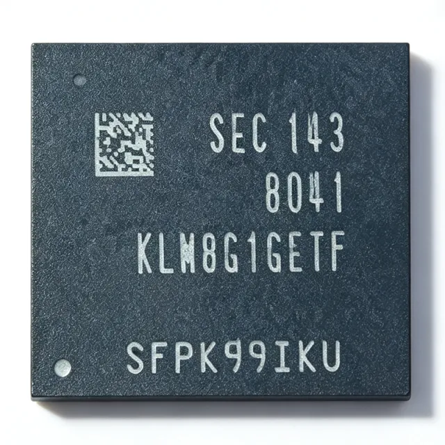
KLM8G1GETF-B041 - 8GB eMMC 5.1 Flash, 153-FBGA | Samsung
KLM8G1GETF-B041

KLM8G1GETF-B041 - 8GB eMMC 5.1 Flash, 153-FBGA | Samsung

The Samsung KLM8G1GETF-B041 is an 8 GB (64 Gbit) eMMC 5.1 embedded flash storage device with MLC NAND, a 3V VDDF (NAND) supply, 1.8V/3V dual VCCQ supply, and a 153-pin FBGA package rated from -25C to +85C. An eMMC (embedded MultiMediaCard) is an embedded flash storage solution that integrates NAND flash die and a standard MMC controller in a single BGA package. It sits within the memory hierarchy as non-volatile embedded storage, managed through the JEDEC-standard MMC protocol v5.1, which presents a simple read/write register interface to the host processor instead of raw NAND management. Key features include eMMC 5.1 specification compatibility, built-in wear leveling, bad block management, ECC error correction, a hardware reset function, and secure write protection. Because the controller handles flash management internally, host software complexity is dramatically reduced compared with raw NAND. Technically, the device exposes a x1 or x4-bit or x8-bit data bus operating under MMC protocol v5.1, with VDDF at 3V for the NAND area and VCCQ at 1.8V or 3V for the interface. Samsung positions its eMMC eSTORAGE family as offering superior power efficiency and fast speed for slim mobile designs. The integrated controller performs erase management, wear leveling, and error correction transparently. Typical applications include smartphone and tablet main storage, smart home and IoT hubs, industrial HMI and data loggers, set-top boxes, and automotive infotainment head units. The 153-FBGA footprint and industry-standard interface allow drop-in swap between compliant 8GB eMMC 5.1 parts. Design consideration: verify the exact FBGA ball-map suffix, because suffix digits such as -B041 versus -B001 can encode different ball grid arrays, making physically incompatible parts that look identical on paper. This page synthesizes distributor pricing, drop-in alternative analysis, lifecycle alerts, and practical migration notes not found in the Samsung datasheet.

USD $22.02 재고 있음
KM416V4104CS-L6 - 4Mx16 EDO DRAM 60ns 3.3V TSOP-50 | Samsung
KM416V4104CS-L6

KM416V4104CS-L6 - 4Mx16 EDO DRAM 60ns 3.3V TSOP-50 | Samsung

The Samsung KM416V4104CS-L6 is a 4M x 16-bit CMOS Dynamic RAM with Extended Data Out (EDO) architecture, organized as 4Mx16 with 4K refresh and housed in a 50-pin TSOP Type II surface-mount package. It operates from a single 3.3V power supply and offers access times of 60ns (denoted by the '-L6' speed suffix) and 50ns (for the '-L5' speed grade variant). An EDO DRAM (Extended Data Out Dynamic Random-Access Memory) is a type of dynamic RAM that extends the period during which output data remains valid by latching the column address on the rising edge of /CAS, effectively enabling a new column access to begin before the previous data has been read. EDO sits in the memory hierarchy between Fast-Page Mode DRAM (FPM) and synchronous SDRAM, and was widely used in mid-1990s PCs, graphics cards, set-top boxes, and embedded systems before SDRAM displaced it. Key features of the KM416V4104CS-L6 include a 4M x 16 organization (64 Mbit total), 4K refresh cycles at 64ms intervals, CMOS low-power design, and TSOP-II packaging optimized for SMT assembly. The L6 grade specifies a 60ns random column access and 30ns page-mode cycle time. The device also supports CAS-before-RAS (CBR) refresh and self-refresh modes, which simplify memory controller design and reduce power consumption in standby. Typical applications for the KM416V4104CS-L6 include legacy PC main memory modules (such as the KMM366F804CS1 8Mx64 DIMM built from eight KM416V4104CS devices), set-top boxes, industrial control systems, point-of-sale terminals, embedded graphics frame buffers, and telecommunications switching equipment. The 16-bit-wide organization is well suited to bus widths common in 1990s-era microcontrollers and DSPs, including Intel i386/i486 and early PowerPC-based designs. When designing with this part, ensure proper decoupling with 0.1 uF and 0.01 uF capacitors placed near the VCC pins, maintain signal integrity on the address/control lines, and respect the 64ms refresh window. Designers should also note that KM416V4104CS-L6 is a mature, obsolete part - active designs should consider SDRAM, DDR, or modern SRAM equivalents. This page synthesizes distributor pricing, drop-in alternative cross-references, and practical design considerations not collected in a single place by the original Samsung datasheet, helping engineers source and qualify second-source options for legacy and EOL systems.

견적 요청 문의하기
KM681000ALT-10L - 128Kx8 5V Low-Power CMOS SRAM | Samsung
KM681000ALT-10L

KM681000ALT-10L - 128Kx8 5V Low-Power CMOS SRAM | Samsung

The Samsung KM681000ALT-10L is a 128K x 8 bit (1 Mbit) high-speed CMOS static random-access memory (SRAM) organized as 131,072 words by 8 bits, fabricated in low-power CMOS technology and supplied in a 5V operating variant. The -10L speed suffix indicates a 100 ns address access time, suitable for cost-sensitive embedded systems where moderate access latency is acceptable. It is part of Samsung's KM681000 family of asynchronous SRAM devices designed for commercial and industrial temperature ranges. A static RAM (SRAM) is a type of volatile semiconductor memory that uses bistable latching circuitry (typically 6 transistors per cell) to store each bit, eliminating the need for periodic refresh cycles required by dynamic RAM (DRAM). SRAM occupies the role of cache, scratchpad, and buffer memory in the broader memory hierarchy: register file -> SRAM cache -> DRAM main memory -> storage. Its random-access nature and byte-level write granularity make it ideal for control logic, lookup tables, and small data buffers where speed and simplicity outweigh density-per-cost. Key features of the KM681000ALT-10L include 128K x 8 organization, 5V single-supply operation, low standby current, fully static operation requiring no clock or refresh, and TTL-compatible I/O. The device supports common asynchronous SRAM control signals (chip enable, output enable, write enable) and operates over commercial (0C to +70C) or industrial (-40C to +85C) temperature ranges depending on the device grade. The 'ALT' suffix denotes a specific package and operating-mode variant within the KM681000 family. Architecturally, the KM681000ALT-10L uses a 6T CMOS SRAM cell array, internal address decoding, and an 8-bit bidirectional data bus. The die is offered in a small-outline surface-mount package to support compact PCB layouts. The asynchronous interface simplifies integration with microcontrollers and legacy logic that do not provide dedicated SDRAM controllers. Typical applications include industrial control PLCs and HMI panels, networking equipment buffer memory, point-of-sale terminals, instrumentation data logging, automotive infotainment subsystems, and legacy embedded computing where deterministic low-latency read/write access and high endurance are required. The wide temperature tolerance and 5V supply simplify designs replacing older SRAMs in long-lifecycle products. When designing with this device, ensure the address and data lines have adequate decoupling near the device and that the chip-enable access timing (tCE) is respected in worst-case read cycles. Designers upgrading from older 5V SRAMs should confirm the pinout matches their existing footprint, as different Samsung speed grades (e.g., -8, -10, -12) share the same functional pinout but differ in access time.

견적 요청 문의하기
KMC7448THX1400ND - 1.4GHz PowerPC G4 MPU 360-FCCBGA | NXP
KMC7448THX1400ND

KMC7448THX1400ND - 1.4GHz PowerPC G4 MPU 360-FCCBGA | NXP

The NXP KMC7448THX1400ND is a PowerPC G4 microprocessor IC from the MPC74xx family delivering 1.4 GHz 32-bit processing performance in a 360-pin FCCBGA (25x25) package. The device operates from a 1.15 V core supply and is qualified for the -40C to +105C industrial temperature range, making it suitable for compute-intensive embedded platforms requiring proven PowerPC instruction-set compatibility. A microprocessor (MPU) is a single-chip CPU that integrates the central processing unit, cache, memory management unit and on-chip peripherals onto a single die; the PowerPC G4 architecture builds on this base with AltiVec/VMX SIMD extensions and superscalar out-of-order execution. The MPC74xx family sits within NXP/Freescale's high-performance PowerPC microprocessor hierarchy, above the MPC7xx line and aligned with infrastructure, networking and aerospace applications that benefit from mature PowerPC software ecosystems. Key features of the KMC7448THX1400ND include: 1.4 GHz core clock, 32-bit PowerPC architecture with AltiVec-compatible SIMD unit, 1.15 V core VDD, on-chip L1/L2 caches, integrated MMU and the standard PowerPC bus interface. The 360-FCCBGA package exposes the full PowerPC address/data bus plus JTAG, system management and interrupt pins, allowing direct attachment to platform ASICs and DDR memory bridges without external glue logic. Typical applications include industrial control and automation systems, aerospace and defense embedded computing platforms, networking and telecommunications infrastructure, and military-grade single-board computers. The wide industrial temperature window and long-life-cycle PowerPC toolchain support position this part for programs requiring 10+ years of supply continuity rather than the latest-edge consumer silicon. When designing with this part, ensure the 360-ball FCCBGA land pattern is routed with the controlled-impedance, matched-length layers specified in the NXP hardware design guide, and provide low-inductance decoupling within 100 mils of each VDD/VSS pair. Designers should also verify the host firmware supports PowerPC little-/big-endian boot and the platform's boot ROM vector configuration. This page synthesizes distributor pricing, real-time stock signals and drop-in alternatives from the same MPC74xx family, plus practical thermal and signal-integrity notes not found in the standalone datasheet.

견적 요청 문의하기
KMPC8313CVRAGDB - PowerQUICC II Pro 400MHz MPU, 516-TEPBGA | NXP
KMPC8313CVRAGDB

KMPC8313CVRAGDB - PowerQUICC II Pro 400MHz MPU, 516-TEPBGA | NXP

The NXP KMPC8313CVRAGDB is a PowerQUICC II Pro microprocessor built on the PowerPC e300c3 core, operating at up to 400 MHz, and housed in a 516-ball TEPBGA package measuring 27x27 mm. The device integrates a 32-bit single-core CPU with a high-performance system bus, dedicated security engine, DDR1/DDR2 memory controller, dual 10/100/1000 Mbps Ethernet MACs (without encryption), USB 2.0, and four DMA channels, making it suitable for cost-sensitive networking and industrial control applications. A microprocessor (MPU) is an integrated circuit that contains the central processing unit of a computer system, executing instructions fetched from memory and orchestrating peripherals through on-chip controllers. Within the broader semiconductor taxonomy, MPUs sit alongside microcontrollers (MCUs), DSPs, and FPGAs as programmable logic devices, and the PowerQUICC II Pro family specifically targets communications infrastructure where integrated Ethernet and DMA offload reduce bill-of-materials cost. Key differentiating features of the KMPC8313CVRAGDB include the non-encryption variant of the MPC8313E (the 'A' designator denotes absence of the security engine), integrated PHY interfaces, hardware packet handling acceleration, and 16-bit DDR2 memory support up to 266 MHz. The 400 MHz core combined with dual Gigabit Ethernet MACs delivers wire-speed forwarding for entry-level routers, switches, and network appliances. The device uses a 32-bit PowerPC e300c3 superscalar core with separate 16 KB instruction and data caches, dual integer units, and a hardware MMU supporting Linux, VxWorks, and other embedded operating systems. The integrated system bus and DMA controller offload data movement from the CPU, leaving more headroom for protocol processing in networking workloads. Typical applications include SOHO routers, residential gateways, industrial Ethernet switches, networked printers, and embedded Linux appliances. Designers choose this part when they need mature PowerPC software support, integrated Gigabit Ethernet, and a long-life-cycle component for industrial designs. When designing with the KMPC8313CVRAGDB, ensure the PCB has a thermal dissipation path through the exposed pad and that the 1.0 mm pitch BGA is assembled by an experienced contract manufacturer. Programmable clocking and configurable SerDes modes require careful reference-clock jitter analysis to meet Ethernet PHY compliance. This page synthesizes distributor stock data, parametric drop-in alternatives, and practical design notes that complement but do not replace the official NXP MPC8313 hardware specifications reference manual for the part.

견적 요청 문의하기
KMPC8315ECVRAGDA - 400MHz e300c3 MPU | NXP | Networking
KMPC8315ECVRAGDA

KMPC8315ECVRAGDA - 400MHz e300c3 MPU | NXP | Networking

The NXP KMPC8315ECVRAGDA is a PowerQUICC II Pro family microprocessor built on the PowerPC e300c3 core running at 400 MHz, packaged in a 620-ball BGA (HBGA, 29x29 mm) with exposed pad. It integrates a 32-bit single core, hardware security (SEC 3.3), DDR/DDR2 memory controllers, and Gigabit Ethernet MACs, targeting embedded networking and secure communications applications. The part ships in tray packaging, is lead-free, and is RoHS3 compliant. A microprocessor (MPU) is an integrated circuit that contains the central processing unit of a computer or embedded system. The PowerQUICC II Pro architecture (MPC83xx) extends the classic PowerQUICC communications-oriented MPU line with integrated security, DDR memory controllers, and enhanced Ethernet support. The 'K' prefix in this MPN indicates a specific NXP/Freescale K-code designation typically tied to a particular speed grade, security revision, or customer-specific configuration; the underlying silicon remains e300c3-based. Key features include a 400 MHz e300c3 core, hardware SEC 3.3 security engine, integrated DDR/DDR2 memory controller with ECC support, multiple 10/100/1000 Ethernet MACs, PCI Express and PCI interfaces, USB 2.0 (host/device), local bus controller, and a wide range of serial peripherals. The device is rated for industrial temperature operation and is targeted at secure networking equipment such as routers, switches, VPN gateways, and industrial control platforms. From an architecture perspective, the e300c3 core uses a 7-stage pipeline with hardware multiply/divide and is binary-compatible with PowerPC Book E instruction set. Combined with the integrated SEC 3.3 engine, the part can accelerate AES, DES/3DES, SHA-1/256, and public-key operations without burdening the core, enabling line-rate encryption on multi-gigabit links. Typical applications include secure routers, VPN/IPsec gateways, industrial Ethernet switches, wireless base-station controllers, and printing/imaging controllers. The integrated security accelerator and DDR2 controller make it particularly suited for networking appliances that demand deterministic throughput and hardware-rooted trust. When designing with the KMPC8315ECVRAGDA, allocate adequate PCB area for the 29x29 mm BGA, follow NXP's thermal/Power design guidelines, and use a multi-layer PCB with continuous power and ground planes under the exposed pad for heat dissipation and signal integrity. JTAG debug access is recommended for bring-up. This page synthesizes distributor stock and pricing, drop-in pin-compatible alternatives, and practical design notes not found in the standalone manufacturer datasheet, giving engineers a single reference for selecting, sourcing, and replacing the KMPC8315ECVRAGDA in legacy and new designs.

견적 요청 문의하기
KMPC8321CVRADDC - PowerPC e300c2 MPU 266MHz 516-PBGA | NXP
KMPC8321CVRADDC

KMPC8321CVRADDC - PowerPC e300c2 MPU 266MHz 516-PBGA | NXP

The NXP KMPC8321CVRADDC is a PowerPC e300c2 based microprocessor (MPU) from the MPC83xx family, integrating one 32-bit core running at 266 MHz in a 516-pin plastic BGA (27 mm x 27 mm) package. The device combines the e300c2 core with the MPC8321E PowerQUICC-style communications engine architecture, including a 32-bit PCI interface, 10/100 Mbps Ethernet MAC, DDR/DDR2 memory controller, and a flexible peripheral set for embedded networking. What is a PowerQUICC MPU? A PowerQUICC (pronounced 'powerquick') microprocessor is a class of Power-Architecture communications processors derived from NXP/Freescale's MPC8xx family, designed around integrated communications peripherals such as Ethernet MACs, PCI, and HDLC channels. In the system hierarchy, the KMPC8321 sits under 'microprocessor -> communications processor -> embedded MPU -> semiconductor IC' and is intended to consolidate a CPU plus communications I/O onto a single die for networking appliances. Key features of the KMPC8321CVRADDC include the PowerPC e300c2 core with MMU and dual-issue capability, a 32-bit PCI 2.3 controller, dual 10/100 Ethernet MACs (one of which is MII/RMII-capable), USB 2.0 (Full-Speed) interface, DDR1/DDR2 SDRAM controller, local bus interface (8/16/32-bit with NAND flash support), four DMA channels, two I2C controllers, two UARTs, and serial peripheral interfaces. The integrated security engine accelerates DES, 3DES, AES, and SHA/MD5 hashing. Architecturally the device uses a 266 MHz core feeding a 32-bit peripheral bus and the integrated peripherals are clocked from independent peripheral clocks synchronized via internal PLLs. The on-chip caches (16 KB instruction / 16 KB data) and the integrated DDR memory controller allow zero-wait-state external memory access in typical embedded configurations, while the BGA package exposes both high-speed peripheral balls and memory/PCI bus balls. Typical applications include small-form-factor routers and gateways, networked attached storage (NAS) controllers, industrial Ethernet bridges, multi-channel VoIP/IP-PBX cards, line cards for access equipment, and printer/scanner MFP controllers where PCI plus Ethernet plus DDR are needed on one chip. When designing with the KMPC8321CVRADDC, follow NXP's hardware design guide for the 516-PBGA - the package requires a multi-layer (typically 6+ layer) PCB with controlled-impedance routing for DDR/PCI, matched-length Ethernet pairs, and extensive thermal vias under the die. Plan power sequencing carefully because the DDR interface requires VTT termination that is referenced to VDDQ. This page synthesizes distributor inventory, drop-in alternatives, and practical design notes not consolidated in the manufacturer datasheet.

견적 요청 문의하기
KMPC8321ECVRAFDC - PowerPC e300c2 MPU, 333MHz, 516-PBGA | NXP
KMPC8321ECVRAFDC

KMPC8321ECVRAFDC - PowerPC e300c2 MPU, 333MHz, 516-PBGA | NXP

The NXP (formerly Freescale) KMPC8321ECVRAFDC is a PowerPC e300c2 microprocessor IC in the MPC83xx PowerQUICC II Pro family, delivering a 32-bit single-core architecture at 333 MHz, housed in a 516-ball Plastic BGA (PBGA) package measuring 27x27 mm. The device integrates a hardware encryption accelerator (the "ENC" suffix designation) and is designed for power-sensitive communications infrastructure where deterministic performance and security offload are required. An MPU (Microprocessor Unit) is a programmable integrated circuit that fetches, decodes, and executes instructions from external memory; embedded MPUs such as this one integrate CPU core, MMU/FPU units, caches, memory controllers, and a rich set of system peripherals onto a single die. The KMPC8321E belongs to a broader taxonomy of PowerPC-based communications processors (e300c2 -> PowerQUICC II Pro -> PowerQUICC family -> Freescale/NXP communications processors -> embedded microprocessors). The "8321" designation identifies it as a low-cost member of the PowerQUICC II Pro line, sitting below the higher-integration MPC8323E and MPC8349E. Key features of the KMPC8321ECVRAFDC include a 333 MHz e300c2 core, hardware encryption acceleration for IPsec/SSL/TLS workloads, dual 10/100/1000 Ethernet MACs with integrated PHYs (via the QUICC Engine UCC), a DDR memory controller, local bus controller (LBC), PCI interface, and a wide range of serial interfaces including UARTs, I2C, and SPI. The part operates from 1.8V/2.5V/3.3V supply rails and is fabricated in a 90 nm CMOS process. Architecturally, the e300c2 core implements the PowerPC ISA with a 16 KB instruction cache and 16 KB data cache, a separate MMU supporting 32-bit virtual addressing, and a dedicated hardware encryption engine capable of offloading DES, 3DES, AES, SHA-1, SHA-256, MD5, and public-key algorithms from the core. The integrated QUICC Engine subsystem provides flexible protocol termination for Ethernet, ATM, HDLC, and UART channels. Typical applications include industrial routers and gateways, network-attached storage (NAS) controllers, secure VPN appliances, DSL/CMTS access equipment, VoIP media gateways, and factory-automation controllers requiring deterministic networking. The hardware encryption accelerator makes it especially attractive for IPsec offload in mid-range VPN concentrators. When designing with this device, ensure that the four-layer (or better) PCB stack-up provides continuous ground references under the 27x27 mm BGA footprint to maintain SI integrity on the DDR memory bus, and validate thermal headroom using the official NXP thermal model - the 516-BGA dissipates appreciable power under full Ethernet and encryption load.

견적 요청 문의하기
KMPC8321EVRADDC - PowerPC e300c2 MPU 266MHz 516-BGA | NXP
KMPC8321EVRADDC

KMPC8321EVRADDC - PowerPC e300c2 MPU 266MHz 516-BGA | NXP

The NXP KMPC8321EVRADDC is a PowerPC e300c2 microprocessor from the MPC8321 PowerQUICC II Pro family, integrating a single 32-bit core running at 266 MHz with hardware encryption acceleration, housed in a 516-pin PBGA package (27x27 mm). A microprocessor (MPU) is a single-chip CPU that integrates the central processing unit, cache, memory management, and peripheral interfaces into one device, sitting at the top of the embedded compute hierarchy (CPU core -> MPU -> SoC -> embedded system). The MPC8321E adds a security engine (SEC 2.0) for DES/3DES/AES/SHA acceleration and is intended for cost-sensitive networking and industrial applications that require cryptography without a dedicated crypto coprocessor. Key features include an e300c2 core with 16 KB L1 instruction cache and 8 KB L1 data cache, a 32-bit DDR/DDR2 memory controller, dual 10/100/1000 Mbps Enhanced Three-Speed Ethernet controllers (eTSECs), a PCI interface, a USB 2.0 (full/low speed) interface, and a peripheral set including DUART, I2C, SPI, and local bus. The integrated security engine accelerates IPSec, SSL/TLS, and SRTP throughput. The MPC8321E is built on a 0.13umCMOS process and operates from a 1.2 V core / 1.8 V / 2.5 V / 3.3 V I/O supply set. The 516-PBGA package provides adequate thermal dissipation for typical 1.5 W to 3 W networking workloads when mounted on a 4-layer PCB with a thermal via array under the exposed die pad. Typical applications include small-office/home-office (SOHO) routers, VPN gateways, industrial Ethernet switches, secure POS terminals, and embedded firewall appliances. The combination of gigabit Ethernet, hardware crypto, and DDR2 support makes it well-suited to wired edge-of-network security devices. When designing with this device, follow the MPC8321E hardware specifications for DDR2 trace length matching (within 50 mils for byte lanes), place 100 nF + 10 uF decoupling on each power rail, and ensure the 66 MHz system clock source meets the jitter requirement stated in the MPC8321E hardware specifications document. Boot configuration is read from reset configuration pins sampled on HRESET negation. This page synthesizes distributor pricing, drop-in alternatives, and practical hardware design notes beyond what the manufacturer datasheet alone provides, including power-on-package thermal guidance and boot-mode strap configuration for production programming.

견적 요청 문의하기
KMPC8321EVRAFDC - PowerPC e300c2 MPU, 333MHz, 516-PBGA | NXP
KMPC8321EVRAFDC

KMPC8321EVRAFDC - PowerPC e300c2 MPU, 333MHz, 516-PBGA | NXP

The NXP KMPC8321EVRAFDC is a PowerPC e300c2 microprocessor from the MPC83xx PowerQUICC II Pro family, integrating a single 32-bit core running at 333 MHz in a 516-pin PBGA package (27 x 27 mm). It combines the e300c2 CPU core with communications-oriented peripherals tailored for networking, telecom, and embedded control applications, and is supplied at a 1 V core voltage. The device belongs to the MPC8321E sub-family which integrates encryption acceleration alongside the QUICC Engine communications controller. An MPU (Microprocessor Unit) is an integrated circuit that contains a central processing unit and tightly-coupled system peripherals, forming the main computational element of an embedded system. PowerQUICC II Pro processors sit in the taxonomy: MPU -> communications processor -> PowerQUICC family -> Power Architecture ecosystem. The PowerPC architecture originated as a RISC design optimized for performance-per-watt, and the e300c2 core used here descends from the Power Architecture embedded lineage commonly used in routers, switches, and industrial control. Key features of the KMPC8321EVRAFDC include the QUICC Engine for hardware-accelerated protocol termination, integrated security engine (typical of the 'E' encryption designation), DDR memory controller, dual 10/100/1000 Ethernet MACs, PCI interface, and a broad set of serial interfaces (UART, I2C, SPI). The 333 MHz core frequency is supported by an integrated memory management unit and L1 cache hierarchy, providing deterministic performance for protocol stacks. Architecturally, the KMPC8321EVRAFDC pairs a 32-bit PowerPC scalar core with a system-on-chip peripheral set on a single die, enabling customers to replace multi-chip designs with a single PBGA device. The 516-PBGA package offers high pin count for parallel external memory and bus interfaces while still being reflow-solderable on standard SMT lines. Typical applications include SOHO/SMB routers, DSL/cable modem gateways, wireless access points, industrial Ethernet bridges, and embedded control with cryptographic requirements. Designers choose this part when they need integrated MACs and a hardware protocol engine rather than an external PHY stack. When laying out the PCB, allocate a continuous copper pour under the exposed die-pad area for thermal dissipation and ground return, and follow NXP layout guidelines for DDR trace length matching. Power-rail decoupling requires a 1 uF + 0.1 uF combination placed within 5 mm of every VDD pin. This page synthesizes distributor stock levels, parameter data, and design notes not found in the manufacturer datasheet alone.

견적 요청 문의하기