제품 (39,000+)

K4S561633FZN75 - 256Mb Mobile SDRAM 4x16Mx16 133MHz FBGA | Samsung
K4S561633FZN75

K4S561633FZN75 - 256Mb Mobile SDRAM 4x16Mx16 133MHz FBGA | Samsung

The Samsung K4S561633F-ZN75 is a 268,435,456-bit synchronous Mobile SDRAM organized as 4 banks x 4,196,304 words x 16 bits, fabricated with Samsung's high-performance CMOS technology and housed in a 54-ball FBGA (54BOC) package. It operates at a 133 MHz clock frequency with a 3.0 V supply, supports LVCMOS-compatible inputs, and is offered in a Pb-free (lead-free) variant under the '-ZN75' ordering code suffix, indicating commercial temperature grade and 133 MHz speed bin. What is Mobile SDRAM? A Mobile SDRAM (Synchronous Dynamic Random-Access Memory) is a low-power variant of standard SDRAM optimized for portable and battery-powered applications. It adds features such as partial-array self-refresh (PASR), temperature-compensated self-refresh (TCSR), and a deep power-down mode that dramatically reduce standby current compared with conventional SDRAM. Within the broader memory taxonomy, Mobile SDRAM sits below LPDDR/DDR but above asynchronous SRAM in performance-per-watt, and is fabricated in the same CMOS process nodes used for commodity DRAM. The 54BOC FBGA package gives a compact 8 mm x 10 mm footprint suitable for handheld product designs. Key features of the K4S561633FZN75 include a fully synchronous operation referenced to a positive-edge clock, programmable CAS latency of 2 or 3, programmable burst length of 1, 2, 4, 8 or full page, and auto-precharge. The 4-bank architecture enables interleaved operations that hide precharge latency, while the LVCMOS interface simplifies connection to mobile ASICs, baseband processors, and application processors from the 2003-2008 generation. The device supports both Auto-Refresh and Self-Refresh modes and includes a power-down mode for additional energy savings. The K4S561633FZN75 is implemented using Samsung's high-performance CMOS process and a twin-cell storage architecture, delivering high data rates at moderate power consumption. Synchronous design allows precise cycle control with the system clock and I/O transactions are possible on every clock cycle, which simplifies controller logic compared with asynchronous DRAMs. Typical applications include mobile phone image buffers, portable media player working memory, PDA / handheld computing buffers, digital camera burst-frame storage, and GPS navigator working memory. The wide operating voltage and low-power modes also make it suitable for industrial handheld terminals and early-generation smart-phone designs. When designing with this part, ensure that the controller drives CK, CKE, CS, RAS, CAS, WE, BA0/BA1, A0-A12, DQ0-DQ15, DQM, and the ZN75-spec power pins according to the datasheet's AC timing table. Decoupling must use 100 nF plus 10 uF per rail within 5 mm of the BGA balls to maintain signal integrity at 133 MHz. This page consolidates distributor pricing, JEDEC-standard Mobile SDRAM cross-references, and design notes specific to 54BOC FBGA layouts, offering information not typically compiled on a single manufacturer datasheet page.

견적 요청 문의하기
K4S641632H-UC75 - 64Mb H-die SDRAM 1M x 16 x 4 Banks | Samsung
K4S641632H-UC75

K4S641632H-UC75 - 64Mb H-die SDRAM 1M x 16 x 4 Banks | Samsung

The Samsung K4S641632H-UC75 is a 64Mb H-die synchronous DRAM (SDRAM) organized as 1M x 16 bits x 4 banks, fabricated with Samsung's high-performance CMOS technology. Housed in a 54-pin TSOP-II Pb-free (RoHS compliant) package, it operates at 133 MHz clock frequency with LVCMOS-compatible inputs and outputs. The device uses a 3.3 V supply, multiplexed address bus, and supports four-bank operation with MRS/EMRS cycles for CAS latency, burst length, and burst type programming. What is SDRAM? Synchronous DRAM is a dynamic random-access memory that synchronizes data transfers with the rising edge of a system clock, enabling higher throughput than asynchronous DRAM. Within the memory hierarchy, SDRAM sits above SRAM and below cache as the main system memory for embedded systems, networking equipment, and consumer electronics. SDRAM evolved into subsequent generations including DDR, DDR2, DDR3, DDR4, and DDR5 SDRAM; the K4S641632H is a first-generation SDR (Single Data Rate) SDRAM. It uses a four-bank architecture to improve throughput by allowing one bank to precharge while another is being accessed. Key features of the K4S641632H-UC75 include a maximum operating current of 135 mA, commercial operating temperature range of 0C to +70C, full-page burst capability, and sequential/interleave burst modes. The 1M x 16 organization is well-suited for 16-bit data buses in legacy embedded designs, while the four-bank architecture supports concurrent activation of up to four rows for higher bandwidth. LVCMOS interface simplifies connection to standard logic-level controllers without level shifters. In terms of architecture, the K4S641632H-UC75 uses a pipelined multi-bank internal structure that supports auto-refresh and self-refresh modes for data retention. The address bus is multiplexed into row and column addresses via RAS#, CAS#, and WE# control lines, reducing pin count and enabling high-density integration in the 54-pin TSOP-II form factor. Typical applications include networking routers, set-top boxes, industrial control equipment, embedded computing platforms, legacy computer main memory, and graphics frame buffers. The 16-bit-wide data bus is a natural fit for embedded processors and DSPs that expect half-word memory accesses. When designing with this device, ensure proper decoupling with 0.1 uF and 0.01 uF capacitors placed close to VDD/VSS pins, follow the standard SDRAM initialization sequence (PRECHARGE -> NOP -> MRS), and respect tRCD/tRP/tRFC timing parameters per the datasheet. This page synthesizes distributor pricing, drop-in alternatives, and practical design notes not found in the manufacturer datasheet alone.

견적 요청 문의하기
K4S641632K-UC75 - 64Mb SDRAM 4Mx16 3.3V 54-TSOP II | Samsung
K4S641632K-UC75

K4S641632K-UC75 - 64Mb SDRAM 4Mx16 3.3V 54-TSOP II | Samsung

The Samsung K4S641632K-UC75 is a 67,108,864-bit synchronous high-data-rate Dynamic RAM organized as 4 banks x 1,048,576 words by 16 bits (4Mx16), fabricated on Samsung's high-performance CMOS process. The device operates from a single 3.3V supply, supports a clock frequency up to 133 MHz (the -UC75 speed grade), and is housed in a 54-pin TSOP-II surface-mount outline. An SDRAM (Synchronous Dynamic Random-Access Memory) is a volatile memory class that synchronizes data transfers to a system clock, enabling burst-oriented read/write cycles. SDRAM sits within the broader hierarchy of memory ICs -> DRAM -> volatile memory -> semiconductor, and is the predecessor to subsequent generations such as DDR, DDR2 and DDR3. The K4S641632K-UC75 is a member of the legacy SDR (Single Data Rate) SDRAM family that dominated main memory from the late 1990s through the early 2000s and remains in use today for legacy industrial, networking and embedded designs. Key features of the K4S641632K-UC75 include a 4-bank architecture with 4096 refresh cycles, programmable CAS Latency (CL=2 or CL=3), a 16-bit data bus, and a 12-bit row address / 8-bit column address multiplexed interface. Auto-refresh and self-refresh modes are supported, along with power-down and clock-suspend functions for reduced quiescent current. The 54-pin TSOP-II package measures approximately 10.16 mm x 22.22 mm with a 0.8 mm pitch and is JEDEC-standard, allowing direct substitution with pin-compatible SDRAMs from Samsung (K-die family), Micron, ISSI and Alliance Memory. The device is rated for commercial temperature range (0°C to +70°C). Typical applications include embedded systems using legacy CPUs (e.g., PowerPC, ARM7/ARM9, MIPS, SH-3), networking line cards, industrial control mainboards, set-top box memory, and printer/copier controller boards that still require 3.3V SDR SDRAM. Many industrial designs retain SDR SDRAM today because of long lifecycle, easy sourcing, and full JEDEC pinout compatibility across vendors. When designing with the K4S641632K-UC75, observe JEDEC SDRAM timing parameters (tRCD, tRP, tRFC, tMRD). A 0.1 uF decoupling capacitor must be placed close to each VDD/VSS pair, and the clock, CKE, and chip-enable signals must be cleanly routed to avoid glitches that can corrupt state. Banks must be properly precharged before issuing new commands. This page synthesizes distributor pricing, drop-in JEDEC alternatives from the same Samsung K-die family, and practical PCB-layout guidance not consolidated in any single manufacturer datasheet, providing a single source for engineers evaluating or replacing the K4S641632K-UC75.

견적 요청 문의하기
K6F1616U6A-EF55T - 16Mbit Async SRAM 55ns 48-TFBGA | Samsung
K6F1616U6A-EF55T

K6F1616U6A-EF55T - 16Mbit Async SRAM 55ns 48-TFBGA | Samsung

The Samsung Semiconductor K6F1616U6A-EF55T is a 16Mbit asynchronous static RAM (SRAM) organized as 1M x16 bits, operating from a single 2.7V to 3.3V supply with a 55ns access time, housed in a 48-ball TFBGA (7.5 x 9.5 mm) package with Tape and Reel delivery. An asynchronous SRAM is a type of volatile semiconductor memory that stores each bit in a bistable latch circuit and does not require a clock signal or periodic refresh, unlike DRAM. Within the memory IC hierarchy, static RAM sits alongside DRAM and non-volatile memory as a parallel-interface memory class, favored where deterministic, low-latency read and write cycles matter more than raw density. Because there is no refresh circuitry, controller design is simplified to standard address, data, and chip-enable strobes. Key features of the K6F1616U6A family include super-low-power full-CMOS construction, a wide 2.7V to 3.3V operating range suited to battery-powered systems, a parallel 16-bit wide data bus, and a compact 48-TFBGA footprint that conserves board area versus legacy TSOP SRAM packages. The 55ns speed grade supports zero-wait-state access from mid-range microcontrollers and DSPs. Technically, the device uses a six-transistor full-CMOS memory cell, which yields near-zero static current in standby when deselected and eliminates refresh overhead entirely. Data is retained as long as supply voltage remains in range, and access is controlled via chip enable, output enable, and write enable signals in a conventional asynchronous SRAM timing scheme. Typical applications include battery-powered portable instrumentation, industrial control panels requiring code or data scratchpad memory, network equipment line-card buffers, and legacy embedded designs replacing older SRAM generations such as the K6X0808/K6X1008 families. Design consideration: use 55ns access timing conservatively - add address-valid setup margin in controller timing loops, and keep the TFBGA land pattern per the datasheet ball map since ball-grid escape routing constrains trace length matching. This page synthesizes distributor availability data, drop-in alternative analysis, and practical design notes not found in the manufacturer datasheet, with pricing freshness as of 2026-09-01.

견적 요청 문의하기
K6F2016U4D-FF70T00 - 2Mbit Async SRAM 70ns 48-FBGA | Samsung
K6F2016U4D-FF70T00

K6F2016U4D-FF70T00 - 2Mbit Async SRAM 70ns 48-FBGA | Samsung

The Samsung K6F2016U4D-FF70T00 is a 2Mbit asynchronous full CMOS static RAM (SRAM) organized as 128K x 16 bits, operating from a 2.7V to 3.3V supply with a 70ns access time (tAA), packaged in a 48-ball FBGA (6x7 mm) chip-scale package. An asynchronous SRAM is a type of random-access memory that does not require a clock signal for read or write operations; data is accessed directly by applying an address on the address bus and activating the chip enable (CE), output enable (OE), and write enable (WE) control pins. Within the memory IC hierarchy, it belongs to the solid-state SRAM class, sitting above DRAM in speed determinism and below synchronous SRAM in density, and is widely used as a power-management-level companion memory for microprocessors and DSPs. Key features of the K6F2016U4D family include super-low-power full CMOS process technology, a wide 2.7V to 3.3V operating voltage range, industrial temperature support, and a compact 48-ball chip-scale package for flexible system design. The 16-bit organization allows word-wide data paths that simplify interfacing to 16-bit processors without external bus-width glue logic. Technically, the device is fabricated on Samsung's advanced full CMOS process, which minimizes standby and operating current. Revision history of the family datasheet notes parameter adjustments such as tWP set to 50ns for 70ns-grade product, indicating active datasheet maintenance. Speed grades of 55ns and 70ns are offered under the FF55 and FF70 suffixes. Typical applications include battery-powered portable instruments, industrial control systems, network equipment buffering, and as code/data scratch memory for FPGAs and microcontrollers that require deterministic, zero-wait-state access. Designers should verify that the 70ns access time meets the system bus timing margin, and should properly terminate unused balls per datasheet guidance. Because the part is offered in a BGA package, X-ray inspection capability is recommended for incoming quality control and rework planning. This page synthesizes distributor availability data, datasheet-derived specifications, drop-in alternative analysis, and design guidance not found in the manufacturer datasheet alone.

견적 요청 문의하기
K6F4016U6E-EF55 - 256Kx16 4Mb Low-Power SRAM 55ns | Samsung
K6F4016U6E-EF55

K6F4016U6E-EF55 - 256Kx16 4Mb Low-Power SRAM 55ns | Samsung

The Samsung K6F4016U6E-EF55 is a 256K x 16-bit (4-Mbit) ultra-low-power, low-voltage, full-CMOS static RAM organized as 4,194,304 bits with a 16-bit data I/O interface, available in a 48-ball Chip Scale Package (CSP/BGA) and access times of 55 ns and 70 ns. It operates from a single 2.7 V to 3.3 V supply, supports an industrial temperature range, and is fabricated on Samsung's advanced full-CMOS process technology for low active and standby current consumption. A Static RAM (SRAM) is a type of volatile semiconductor memory that stores each bit in a pair of cross-coupled inverters (a flip-flop) rather than a capacitor, giving it infinite read/write endurance and zero refresh requirement. The K6F4016U6E-EF55 belongs to the asynchronous SRAM category, where read/write operations are controlled by the chip enable (/CE), write enable (/WE), and output enable (/OE) signals without an internal clock. SRAM sits in the memory hierarchy between DRAM (higher density but needs refresh) and register files (faster but lower density), and is preferred in systems where deterministic access time, low power, and high reliability outweigh density cost. Key features include a wide 2.7 V to 3.3 V Vcc operating range, low standby current typical of full-CMOS 6T cell design, three-state common I/O, fully static operation requiring no clock or refresh, and CMOS- and TTL-compatible I/O levels. Byte-wise control via upper-byte (/UB) and lower-byte (/LB) signals enables 8-bit and 16-bit access on the same device, while the 48-CSP package offers a small footprint suited to space-constrained handheld and embedded boards. Typical applications include handheld and battery-operated terminals, industrial controllers and PLCs, metering and instrumentation data buffers, networking line cards, automotive infotainment buffers, and other embedded designs where 4 Mbit of non-volatile-friendly scratch memory is required. Designers choose the trio: 55 ns access makes the device compatible with most low-to-mid-speed microcontrollers without wait generation, and the wide 2.7 V to 3.3 V range allows direct connection to a single Li-ion or 3.3 V regulated rail. When designing with this device, observe the derating for output loading (lumped vs distributed capacitive loads) and follow the recommended decoupling scheme. Place a 0.1 uF ceramic bypass capacitor as close as possible to the Vcc ball, and add a bulk 1 uF to 10 uF capacitor if multiple SRAMs share the supply rail. The chip-scale package also requires IPC-7351-compliant land pattern with NSMD pads for reliable assembly. This page synthesizes distributor pricing, drop-in alternates, and practical design considerations that are not present in the bare Samsung datasheet, including a side-by-side same-family comparison and cross-brand SRAM substitutes.

견적 요청 문의하기
K6T0808C1D-DB55 - 32Kx8 Low Power CMOS SRAM | Samsung
K6T0808C1D-DB55

K6T0808C1D-DB55 - 32Kx8 Low Power CMOS SRAM | Samsung

The Samsung K6T0808C1D-DB55 is a 32K x 8 bit (256 Kbit) Low Power CMOS Static RAM fabricated on Samsung's advanced CMOS process technology, housed in a 28-pin TSOP1F (Type I, forward) surface-mount package with a 70 ns access time grade and an industrial operating temperature range from -40 C to +85 C. A Static RAM (SRAM) is a type of volatile semiconductor memory that retains stored data as long as power is applied, without requiring periodic refresh cycles. SRAM sits in the broader memory hierarchy above DRAM because it offers faster access and simpler control logic, but at higher cost per bit. The 32K x 8 organization yields 32,768 addressable bytes accessed through 15 address lines and 8 bidirectional data lines, which is the classic 28-pin asynchronous SRAM pinout used for nearly three decades in routers, printers, industrial controllers, and legacy embedded systems. Key features include a 70 ns maximum access time (TA = 70 ns grade), low standby current of typically a few microamperes (data-retention mode), single 5 V power supply operation, fully static operation requiring no clock or refresh, TTL-compatible I/O levels, and three-state output drivers that allow direct bus connection. The -DB55 ordering suffix encodes the package style (TSOP1F), the 70 ns speed grade, and the -40 C to +85 C industrial temperature range. The K6T0808C1D family is fabricated with Samsung's high-density CMOS cell design and incorporates on-chip bias generation for stable read/write margins across the full temperature range. The architecture supports common SRAM control signals including Chip Enable (CE), Output Enable (OE), and Write Enable (WE), with byte-wide data access through eight bidirectional DQ pins, providing compatibility with 8-bit microcontrollers, DSPs, and legacy CPU buses. Typical applications include router and switch packet buffers, industrial PLC working memory, printer image data buffers, barcode scanner local memory, instrumentation data loggers, legacy 8-bit and 16-bit microcontroller expansion memory, and battery-backed configuration parameter storage. The wide industrial temperature window also makes it suitable for outdoor telecom equipment and automotive infotainment subsystems. When designing with this device, decouple VCC with a 0.1 uF ceramic capacitor placed within 5 mm of the supply pin and add a 10 uF bulk tantalum or ceramic capacitor on the same rail. Tie unused input pins such as CE, OE, or WE to a defined logic level to avoid spurious read/write cycles from floating CMOS inputs. This page synthesizes distributor pricing, drop-in alternatives, and practical design notes not found in the manufacturer datasheet alone.

견적 요청 문의하기
K6T0808C1D-DB70 - 256Kbit (32Kx8) CMOS SRAM 70ns DIP-28 | Samsung
K6T0808C1D-DB70

K6T0808C1D-DB70 - 256Kbit (32Kx8) CMOS SRAM 70ns DIP-28 | Samsung

The Samsung Semiconductor K6T0808C1D-DB70 is a 256Kbit (32K x 8) low-power CMOS static RAM organized as 32,768 words by 8 bits, with a 70 ns access time, housed in a 28-pin through-hole DIP (DIP-28, 'DB' package code) for commercial-grade (0C to +70C) operation. The K6T0808C1D family consists of asynchronous, byte-wide static RAM cells fabricated on Samsung's advanced CMOS process technology. A static RAM (SRAM) is a type of volatile semiconductor memory that retains data bits as long as power is supplied, without refresh cycles, and uses a bistable latch (cross-coupled inverters) per cell. SRAM occupies the latency tier between faster register files and slower dynamic RAM (DRAM), making it the standard choice for cache memories, look-up tables, FIFOs, and embedded scratch-pad memory in microcontrollers and ASICs. The K6T0808C1D sits within the broader memory taxonomy: SRAM -> volatile memory -> semiconductor memory -> integrated circuit. Key features of the K6T0808C1D-DB70 include a single 4.5 V to 5.5 V power supply, typical operating current of 60 mA, and a standby current of 15 uA at full data retention. The device offers a TTL-compatible parallel interface with three-state outputs, an active-low chip enable (CE1) and active-high chip enable (CE2) for memory expansion, an active-low output enable (OE) for bus arbitration, and an active-low write enable (WE) for read/write control. The DB package denotes the 600-mil wide DIP-28 form factor with through-hole leads, which simplifies prototype bring-up and is often used as a one-for-one retrofit for legacy 32Kx8 SRAM sockets. The K6T0808C1D architecture uses a 6-transistor (6T) full CMOS memory cell, which delivers low standby current, fast access, and high noise immunity relative to older NMOS designs. The -DB70 speed code indicates a 70 ns address access time (tAA) and supports 55 ns and 70 ns grades across the family. The 'C' suffix in the family name signifies the commercial 0C to +70C temperature range, while the 'D' indicates DIP packaging. Typical applications include legacy industrial controller scratch-pad memory, instrument data buffers, programmable logic controller (PLC) bit/byte storage, point-of-sale terminal transaction buffers, telecom line-card buffer memory, and retrofit of older 32Kx8 SRAM sockets in vintage computer or test equipment boards. The DIP-28 package also makes the K6T0808C1D-DB70 popular for educational, hobbyist, and breadboard-based designs. When designing with this SRAM, observe bus contention rules: never assert WE and OE simultaneously while the output drivers are enabled. Add 0.1 uF decoupling close to each VCC pin and a bulk 10 uF capacitor on the supply rail to suppress switching transients on read/write cycles. This page synthesizes distributor availability, drop-in pin-compatible alternatives, and practical design considerations that go beyond the manufacturer datasheet.

견적 요청 문의하기
K6T1008C2E-GB70 - 128Kx8 SRAM, 70ns, 5V CMOS | Samsung
K6T1008C2E-GB70

K6T1008C2E-GB70 - 128Kx8 SRAM, 70ns, 5V CMOS | Samsung

The Samsung K6T1008C2E-GB70 is a 128K x 8-bit Low Power CMOS Asynchronous Static RAM (SRAM) organized as 1 Mbit of memory with a 70 ns access time, packaged in a 32-pin Small Outline Package (SOP-32). It operates from a single 4.5 V to 5.5 V supply, with 50 mA typical operating current and CMOS-compatible standby current well under 1 mA. The device is fabricated on Samsung's low-power CMOS process that uses six-transistor (6T) memory cells with full CMOS periphery, eliminating the need for external refresh. An SRAM (Static Random-Access Memory) is a type of volatile semiconductor memory that stores each bit in a bistable latch, retaining data as long as power is applied without any refresh cycles. SRAMs are positioned in the memory hierarchy between high-density DRAM (which requires refresh) and fast register files (which are too small for general storage). Within the broader taxonomy, SRAM is a member of the volatile memory IC family, which in turn belongs to memory and storage semiconductors. The K6T1008C2E is part of Samsung's legacy K6T family of asynchronous SRAMs, which has been widely second-sourced and is considered an industry-standard pinout. Key features of the K6T1008C2E-GB70 include fully static operation requiring no clock or refresh, three-state common I/O, TTL-compatible inputs and outputs, and a single Chip Enable (CE) pin plus Output Enable (OE) for bus control. The 70 ns access time (tAA) makes it suitable for moderate-speed microcontroller and embedded processor bus interfaces. The SOP-32 surface-mount package provides a low-profile footprint compatible with standard 32-SOIC land patterns, simplifying PCB layout. The device is offered in commercial (C) and industrial (I) temperature grades, with the -GB suffix denoting SOP-32 package, lead-free, and 70 ns speed bin. Typical applications include industrial controllers, firmware boot memory, embedded data logging, computing modules, and replacement sourcing for obsolete systems. The wide 5 V supply range and TTL compatibility make it ideal for legacy 5 V microcontrollers and 8/16-bit processor buses where modern synchronous SRAMs are not required. The asynchronous interface simplifies the memory controller design, eliminating the need for clock-aligned control logic. When designing with this part, verify the tAA timing budget against the host processor's memory cycle time. At 70 ns access time, the part is best suited for host buses running at 14 MHz or lower. For higher performance buses, consider a 55 ns variant or move to a synchronous SRAM. Decoupling with a 0.1 µF ceramic capacitor placed within 5 mm of the VCC pin is recommended for stable operation.

견적 요청 문의하기
K6X1008C2D-BF55 - 128Kx8 Low Power CMOS SRAM | Samsung
K6X1008C2D-BF55

K6X1008C2D-BF55 - 128Kx8 Low Power CMOS SRAM | Samsung

The Samsung K6X1008C2D-BF55 is a 128K x 8 bit (1 Mbit) low-power CMOS asynchronous Static RAM housed in a 32-pin SOP-525 surface-mount form factor. It operates from a single 5 V supply and offers a 55 ns access time, targeting battery-backed and industrial embedded systems where non-volatile storage is unavailable or undesirable. The device uses six-transistor (6T) CMOS memory cells with a fully static interface that requires no clock or refresh. A Static RAM (SRAM) is a type of random-access memory in which each bit is stored in a latch made of cross-coupled inverters, allowing data to be retained as long as power is applied without the periodic refresh cycles demanded by DRAM. In the broader taxonomy, SRAM sits under volatile memory, which itself belongs to the memory IC hierarchy under integrated circuits. The K6X1008C2D-BF55 uses this architecture to deliver fast, deterministic access times suited to control-plane rather than bulk-storage workloads. Key features include a 55 ns access time, low operating current of approximately 30 mA, low standby current, and full CMOS input/output compatibility with TTL-level thresholds. The wide 32-pin SOP footprint supports easy hand-soldering and inspection for low-volume industrial assemblies and legacy retrofits. The part supports standard asynchronous SRAM control signals including /CE (Chip Enable), /OE (Output Enable), and /WE (Write Enable), enabling a glue-less interface to most microcontrollers and microprocessors without external glue logic. The device architecture relies on a conventional six-transistor memory cell array organized as 131,072 bytes, addressable through 17 address lines and an 8-bit bidirectional data bus. A single 5 V rail powers both the array and the I/O, and internal address latches keep the array stable after the falling edge of /CE, simplifying read-modify-write operations. This asynchronous design avoids the timing-sensitive clock trees found in synchronous SRAMs, allowing direct 8-bit microcontroller attachment without bus-turnaround sequence management. Typical applications include industrial controllers, embedded firmware boot buffers, data loggers, point-of-sale terminals, and legacy computing modules. The K6X1008C2D-BF55 also fits well in PLCs, instrumentation data buffers, and replacement-sourcing scenarios where Samsung's mature K6X1008C2D family is the incumbent part. When designing with this device, ensure /CE, /OE, and /WE timing follows the asynchronous SRAM protocol specified in the manufacturer datasheet to avoid bus collisions during read-modify-write cycles. Decoupling the 5 V supply close to the VCC pins with a 0.1 uF ceramic capacitor is strongly recommended. This page synthesizes distributor pricing, drop-in alternatives from the K6X1008C2D family, and practical design notes not found in the original Samsung datasheet, supporting engineers sourcing a 5 V parallel SRAM today.

견적 요청 문의하기
K6X1008C2D-BF70 - 128Kx8 70ns Low Power CMOS SRAM | Samsung
K6X1008C2D-BF70

K6X1008C2D-BF70 - 128Kx8 70ns Low Power CMOS SRAM | Samsung

The Samsung K6X1008C2D-BF70 is a 128Kx8-bit (1 Mbit) asynchronous low-power CMOS Static RAM organized as 131,072 words by 8 bits, providing 70 ns access time in a 32-pin SOP (PDSO32) surface-mount package. It operates from a single 5 V supply and supports full CMOS interfacing with standard TTL-compatible I/O levels. An SRAM (Static Random Access Memory) is a type of volatile semiconductor memory that stores each data bit in a bistable flip-flop cell made of cross-coupled CMOS inverters. Unlike DRAM, SRAM does not require periodic refresh, which simplifies system design and yields deterministic, very low-latency read/write cycles. SRAM is hierarchically positioned as volatile memory, sibling to DRAM and flip-flop based register files, and is typically used for caches, look-up tables, FIFOs, and boot/parameter storage in embedded systems. Key features of the K6X1008C2D-BF70 include 70 ns access time, fully static operation (no clock or refresh required), TTL-compatible I/O, low standby current, and three-state outputs for bus-sharing. The BF70 suffix denotes the 70 ns speed grade in the 32-SOP-525 commercial package with lead-free finish. Operating current (ICC) and CMOS standby current (ICC2) are characterized per the Samsung datasheet revision history. The device uses a six-transistor CMOS memory cell array with conventional address-decoded word-line drivers and sense amplifiers. The asynchronous interface provides a Chip Enable (CE), Write Enable (WE), and Output Enable (OE) control set, allowing the part to drop into industry-standard 128Kx8 SRAM sockets with no firmware changes. Typical applications include data storage in industrial controllers, firmware/parameter boot storage in embedded modules, data logging buffers, computing subsystems, replacement sourcing for legacy 128Kx8 SRAM, and telecommunications equipment. The 32-SOP footprint is convenient for board-level upgrades and last-time-buys. When designing with this part, derate access time budget for temperature and supply variation; place a 0.1 uF decoupling capacitor close to VCC and consider a bulk 1 uF to support read/write peaks. Confirm pinout against the BF70 variant SOP outline (32-SOP-525) rather than the TSOP1 reverse option, because the SOP and TSOP1 pin assignments are not identical. This page synthesizes distributor pricing, drop-in alternatives, and practical design notes not found in a single manufacturer datasheet view.

견적 요청 문의하기
K6X1008C2D-GF70 - 1Mbit 70ns 32-SOP Low Power SRAM | Samsung
K6X1008C2D-GF70

K6X1008C2D-GF70 - 1Mbit 70ns 32-SOP Low Power SRAM | Samsung

The Samsung K6X1008C2D-GF70 is a 128K x 8 bit (1 Mbit) low-power CMOS static RAM (LPSRAM) with 70 ns access time, housed in a 32-pin SOP (PDSO32) plastic surface-mount package. It operates from a single 4.5 V to 5.5 V supply, drawing 35 mA active and supporting a low data-retention voltage for battery-backup operation. The "GF" suffix denotes the 32-SOP commercial-grade package, while "70" indicates 70 ns access time. According to the manufacturer datasheet, the K6X1008C2D family is fabricated using Samsung's advanced full CMOS process, delivering CMOS-compatible inputs/outputs, three-state outputs, and TTL-compatible interface levels. A static RAM (SRAM) is a type of volatile memory that stores each bit in a six-transistor (6T) latch cell, retaining data as long as power is applied without refresh cycles. SRAM occupies the top tier of memory speed in the storage hierarchy (register -> cache -> SRAM -> DRAM -> NAND flash), making it the preferred choice when deterministic, low-latency read/write access is required. The "low-power CMOS" designation places the K6X1008C2D family in the sub-category of asynchronous SRAMs optimized for battery-backed and standby-sensitive applications, sitting between high-speed cache SRAM and DRAM in both cost and density. Key features of the K6X1008C2D-GF70 include 70 ns access time, low data-retention current at 2 V for backup, full CMOS six-transistor memory cell, three-state bidirectional I/O, and a Chip Enable (CE) pin for power gating. The device supports both commercial and industrial operating temperature ranges, and a wide range of package options including 32-SOP, 32-TSOP, and 28-DIP. The simple, asynchronous interface requires no clock or refresh controller, allowing direct connection to a microcontroller bus or address/data latch with minimal glue logic. Typical applications for the K6X1008C2D-GF70 include embedded firmware buffering, industrial controller parameter storage, point-of-sale terminals, portable data loggers, and battery-backed configuration memory. The 32-SOP footprint is the most common of the family and is widely used in industrial and consumer designs where moderate density and low standby power are required. When designing with this part, ensure VCC decoupling of 0.1 uF ceramic close to the supply pin, and observe the derating for I/O loading above 50 pF. For battery-backup designs, hold CE HIGH during VCC ramp-down to enter standby and minimize retention current to a few microamps. Where higher speed (55 ns) or different pinouts are required, consult the K6X1008C2D family ordering matrix. This page synthesizes distributor pricing, drop-in alternative MPNs, and practical design notes that are not consolidated in any single vendor catalog, helping engineers quickly evaluate the K6X1008C2D-GF70 for new designs and legacy replacements.

견적 요청 문의하기
K6X1008C2D-TF55 - 1Mbit 128Kx8 SRAM 55ns 5V | Samsung
K6X1008C2D-TF55

K6X1008C2D-TF55 - 1Mbit 128Kx8 SRAM 55ns 5V | Samsung

The Samsung Semiconductor K6X1008C2D-TF55 is a 1 Mbit asynchronous SRAM organized as 128K x 8 bits, fabricated in Samsung's low-power full CMOS process, with a 55 ns access time, 4.5 V to 5.5 V supply range, and a 32-pin TSOP REVERSE surface-mount package. An asynchronous static random access memory (SRAM) is a type of volatile semiconductor memory that stores each bit in a bistable latch circuit made of cross-coupled inverters. Unlike DRAM, SRAM requires no refresh cycles, and unlike synchronous memories such as SDRAM, it needs no clock: data is accessed whenever address and control signals (CE, OE, WE) are asserted. In the memory hierarchy, SRAM sits at the top for speed and simplicity, making it a staple in embedded systems, industrial controllers, and legacy 5 V buses. Key features of the K6X1008C2D include the 55 ns address access time (tAA), a low operating current of 35 mA, and full CMOS technology delivering very low standby power. The byte-wide 128K x 8 organization maps directly onto 8-bit and 16-bit microprocessor external buses with simple glue logic. The device is built on Samsung's advanced CMOS process, which keeps static power consumption minimal while maintaining fast, uniform access times across the full 4.5 V to 5.5 V industrial supply band. The REVERSE TSOP pinout (32-TSOP REVERSE) places pins in mirrored order versus standard TSOP, so footprint orientation must be checked during layout. Typical applications include industrial PLC memory expansion, legacy networking equipment, telecom line cards, test instrumentation, and replacement/upgrades in service parts for 5 V embedded designs. A key design consideration is supply tolerance: the part requires a regulated 5 V rail within 4.5 V to 5.5 V, so it cannot be dropped into 3.3 V systems without level shifting. This page synthesizes distributor pricing, drop-in alternatives, and practical design notes not found in the manufacturer datasheet.

견적 요청 문의하기
K7A163631B-QI20 - 512Kx36 Sync Pipelined Burst SRAM | Samsung
K7A163631B-QI20

K7A163631B-QI20 - 512Kx36 Sync Pipelined Burst SRAM | Samsung

The Samsung Semiconductor K7A163631B-QI20 is a 512K x 36-bit Synchronous Pipelined Burst SRAM organized as 18,874,368 bits (18 Mb) of high-performance CMOS static RAM. Housed in a 100-pin TQFP package, the device targets Level-2 cache applications in Pentium, PowerPC, and similar high-performance processor-based systems, and delivers synchronous pipelined burst operation with on-chip register-based data alignment. A Synchronous SRAM (Static Random Access Memory) is a type of volatile memory that latches control, address, and data inputs on the rising edge of a system clock. Within the memory taxonomy it sits above DRAM in speed hierarchy but below cache-SRAM in integration; pipelined-burst variants add internal staging registers that allow a new address to be captured every clock cycle while a previous read is completing, dramatically improving throughput at high clock rates compared with standard async or flow-through SRAM. Key specifications for the K7A163631B-QI20 include the 512K x 36 organization (36-bit-wide data bus suited to parity/ECC-protected cache lines), single +3.3 V power supply, low-power CMOS process technology, common I/O data bus architecture, and registered (registered-clock / registered-enable) control inputs that reduce system-clock loading in cache arrays. Burst-mode read and write cycles, byte-write enable controls (typically via BYTE WRITEs x4 with low-byte and high-byte enables), and an output-enable / chip-enable control set are standard on this generation of Samsung B-die synchronous SRAM. Architecturally, the K7A163631B implements an internal 2-stage pipeline: an address register followed by a data-output register, so the first access latency is one extra cycle but subsequent burst beats return every clock. The device supports linear burst order, write-per-bit byte masking, and on-chip clock-domain registers that simplify interface to 66-150 MHz host buses. Power-saving features include CMOS-rail input levels, low standby current, and a chip-enable-controlled power-down mode. Typical applications include Level-2 cache for Pentium II/III class processors, embedded CPU main memory in networking line cards, RAID controller write buffers, networking router/switch control-plane memory, industrial PC cache subsystems, and instrumentation DSP scratchpad memory. The wide x36 bus makes it especially attractive where parity or ECC bits are stored alongside each 32-bit word. A key design consideration is the trade-off between pipelined SRAM (higher sustained throughput, one-cycle additional first-access latency) versus flow-through SRAM (no pipeline, lower latency, lower bandwidth). Choose K7A163631B when the host CPU/cache controller can absorb the one-cycle latency penalty in exchange for higher MHz operation. This page synthesizes distributor pricing, drop-in same-package alternatives, and practical design considerations not found in the Samsung datasheet alone, helping engineers evaluate the part for new designs and legacy second-source supply.

견적 요청 문의하기
K9F1208U0B-JIB0 - 64Mx8 512Mb NAND SLC, TSOP-I-48 | Samsung
K9F1208U0B-JIB0

K9F1208U0B-JIB0 - 64Mx8 512Mb NAND SLC, TSOP-I-48 | Samsung

The Samsung K9F1208U0B-JIB0 is a 64M x 8 bit (512 Mbit total, with an additional 16 Mbit spare area) NAND Flash memory in a 48-pin TSOP-I package (JIB0 suffix), operating from a single 2.7 V to 3.6 V Vcc rail. It uses single-level cell (SLC) NAND technology and delivers a typical 528-byte page read/program architecture with 32-byte spare regions per page, organized as 16-byte × 32 KiB blocks. Sequential page-read access time is on the order of 60 ns and the device supports the legacy 8-bit asynchronous NAND interface (CE, RE, WE, ALE, CLE, WP, R/B) for connection to virtually any microcontroller, ASIC, or dedicated flash controller. What is a NAND Flash Memory IC? A NAND Flash memory is a non-volatile storage device that retains data without power and uses a serialized cell array (NAND string) to deliver higher density and lower cost-per-bit than NOR Flash. Within the memory IC hierarchy, NAND sits under non-volatile memory → flash memory → solid-state storage. NAND parts are typically used for bulk data storage (firmware images, file systems, multimedia buffers) rather than execute-in-place code, and they require an external controller or software layer to perform bad-block management, wear-leveling, and ECC. SLC variants like the K9F1208U0B-JIB0 trade density for higher endurance (~100 k erase cycles per block) and faster write/erase timing than MLC/TLC counterparts, making them ideal for industrial boot, logging, and embedded OS workloads. Key features of the K9F1208U0B-JIB0 include: 528-byte main + 16-byte spare page, 32 KiB (16 KiB × 2) block erase granularity, 10 ms typical block erase time, 200 µs typical page program time, on-chip page buffer for cache-style read/program operations, hardware WP# pin for write-protect during power transitions, and a Ready/Busy# open-drain output for polling-free controller handshaking. Power-down in-flight protection is provided via the WP# pin and an internal data-protection state machine. The TSOP-I-48 package is 18.4 mm × 12.0 mm × 1.0 mm, pin-compatible with the industry-standard TSOP-I NAND footprint. Architecture details: the K9F1208U0B-JIB0 family uses a Samsung NAND cell with a charge-trap floating gate. The controller interface uses command-driven register loading via CLE/ALE signals, with 4-cycle addressing for the legacy 528-byte page (1 cycle column, 3 cycles row). An on-chip page register acts as both data source for read and data sink for program. The device supports copy-back programming for efficient block management without external buffer memory. Typical applications include industrial controllers, embedded Linux/Windows CE boot media, data loggers, set-top box firmware storage, printer consumables, MP3/multimedia recorders, and replacement sourcing for legacy 3.3 V NAND designs. The wide 2.7–3.6 V supply range allows direct connection to a 3.3 V system rail with no level translation. Design tip: pair the K9F1208U0B-JIB0 with a 1 kΩ pull-up on R/B# and a 10 kΩ pull-up on WP# to Vcc; route CE to a dedicated GPIO so partial-array power-down is possible; and always reserve 8 bytes per 528-byte page for hardware ECC (Hamming or BCH). This page synthesizes distributor pricing, drop-in alternatives, and practical design notes not found in the manufacturer datasheet alone.

견적 요청 문의하기
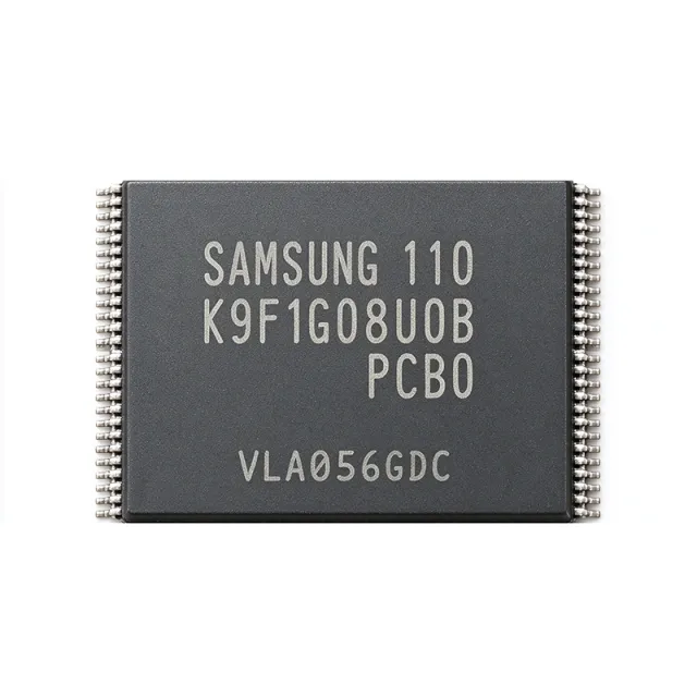
K9F1G08U0B-PCB0 - 1Gbit SLC NAND Flash 3.3V 48-TSOP | Samsung
K9F1G08U0B-PCB0

K9F1G08U0B-PCB0 - 1Gbit SLC NAND Flash 3.3V 48-TSOP | Samsung

The Samsung K9F1G08U0B-PCB0 is a 1 Gbit (128M x 8 bit) single-level-cell (SLC) NAND Flash memory with 32 Mbit spare area, housed in a 48-pin TSOP-I (Type I) surface-mount package and operating from a single 3.3 V supply. It uses an 8-bit parallel I/O bus for address, data and command transfer, eliminating the need for a separate address latch and reducing pin count versus legacy NOR/x16 solutions. The NAND cell array delivers the most cost-effective non-volatile storage density per die area, making this part a mainstay for embedded boot, firmware and data-logging subsystems. A NAND Flash memory is a non-volatile storage IC that arranges memory cells in a NAND (NOT-AND) string topology, where cells are connected in series between bit-line and source-line. Compared with NOR Flash, NAND Flash offers higher density, lower cost per bit, and faster sequential write/erase, at the expense of random read access and byte-level programmability. NAND hierarchy: SLC (1 bit/cell, highest endurance/reliability) -> MLC -> TLC -> QLC. K9F1G08U0B belongs to the SLC tier, the most robust and longest-endurance variant, well suited for industrial, automotive and mission-critical embedded use. Key features of the K9F1G08U0B-PCB0 include 1 Gbit user density plus 32 Mbit spare for ECC and bad-block management, page size 2 Kbyte + 64 byte spare, block size 128 Kbyte + 4 Kbyte spare, typical page program time 200-300 us and block erase time approximately 2 ms. The interface supports CE#, RE#, WE#, ALE, CLE and WP# control lines plus an 8-bit multiplexed I/O bus, compatible with the ONFI 1.0 / legacy Samsung command set. Endurance is specified at 100 K program/erase cycles per block with 10-year data retention. Architecturally, the device integrates a charge-pump-based high-voltage generator, a temperature-compensated sense amplifier array, an internal data register for page buffering, and an ECC-friendly spare area layout. The TSOP-I package exposes all 48 signals with a 0.5 mm pitch, enabling standard SMT reflow and standard 48-TSOP NAND socket compatibility for prototype programming. Typical applications include solid-state data storage in embedded Linux/Windows CE devices, industrial controllers and HMI panels, set-top box firmware storage, networking equipment boot and logs, point-of-sale terminals, eMMC alternative designs, and legacy embedded systems that require raw NAND access via a microcontroller FSMC/NAND controller. A key design consideration when using the K9F1G08U0B-PCB0 is mandatory ECC - the part does not embed on-die ECC for older Samsung K9F families, so the host controller (typically a SoC or FPGA) must run Hamming, BCH or LDPC ECC over each 2 Kbyte page to guarantee data integrity. Initial bad-block marking per Samsung datasheet must also be respected at first power-up. This page synthesizes distributor pricing, drop-in alternatives in the same TSOP-I 48 footprint, and practical design notes not found in the manufacturer datasheet.

USD $2.70 재고 있음
K9F2808UOC-PCB0 - 16M x 8 NAND Flash, 48-TSOP I | Samsung
K9F2808UOC-PCB0

K9F2808UOC-PCB0 - 16M x 8 NAND Flash, 48-TSOP I | Samsung

The Samsung Semiconductor K9F2808UOC-PCB0 is a 16M x 8-bit NAND Flash memory device organized as 16,777,216 bytes (128 Mbit) per chip, supplied in a 48-pin TSOP Type I (or 63-ball TBGA / 48-WSOP1) package option set and operating from a single 2.7 V to 3.6 V rail with a typical access speed of 50 ns. The -PCB0 suffix designates a specific Samsung ordering/lead-finish code within the K9F2808U0C family and shares the same die revision as the parent part, making it pin-compatible across the TSOP-I, WSOP1, and TBGA package options listed in the Samsung datasheet. The part uses the standard 8-bit I/O NAND command set with CLE (Command Latch Enable), CE#, WE#, RE#, and ALE (Address Latch Enable) control lines, plus an R/B# (ready/busy, open-drain) status pin, and supports page sizes of 528 bytes (main 512 + spare 16) typical for SLC NAND of this generation. Program and erase operations are page and block-based respectively, and the internal controller performs automatic block erase, page program, and read with on-chip error management per the ONFI-style command set used by Samsung's 2nd-generation 16Mx8/32Mx8 devices. A NAND Flash memory is a non-volatile storage technology that retains data after power removal using floating-gate transistor cells arranged in a NAND (NOT-AND) string topology, as opposed to the NOR topology used in code-storage flash. NAND Flash belongs to the broader hierarchy: NAND Flash -> Flash Memory -> Non-Volatile Memory -> Semiconductor Memory -> Integrated Circuit. It is the dominant storage technology for high-density applications (USB drives, eMMC, SSDs, memory cards) because of its small cell size (typically ~0.25 um^2 for 50 nm-class SLC), high endurance to program/erase cycles (SLC ~100k cycles per block), and low cost per bit compared to NOR Flash. The K9F2808U0C series was an early-generation small-density NAND Flash primarily used as a boot medium or parameter store in embedded systems. Key features include: 2.7 V to 3.6 V single-supply operation (compatible with 3.3 V system rails), 50 ns read access time, 528-byte page size (512 + 16 spare), 16K-byte block size (16 pages per block, 32 KiB / 16 pages + spare), hardware data protection during power transitions, and an open-drain R/B# output for hardware polling of internal operation status. The device supports standard NAND command set (00h/01h/10h/30h/60h/D0h/50h) for read/program/erase operations. From a technical depth standpoint, the K9F2808U0C family uses Samsung's 2nd-generation NAND process node with single-level cell (SLC) storage; each memory cell stores one bit using a floating-gate transistor. The 528-byte page with 16-byte spare area is the legacy small-page (SLC) NAND layout (sometimes referred to as x8 small-page NAND), and the on-die charge pump generates the high voltages required for program (VPP ~20 V internally) and erase operations from the single 3.3 V VCC supply, eliminating the need for an external high-voltage pump on the system side. The device supports sequential row-address (page) and column-address (byte within page) cycles via the I/O bus while CLE and ALE are toggled. Typical applications include set-top box firmware storage, MP3 player media storage, digital camera image buffer, USB flash drive controllers (as the memory element), embedded Linux boot/rootfs medium in early-generation ARM/MIPS designs, and industrial data logging with wear-leveling FTL in the host controller. The 128 Mbit capacity is well-suited for code-shadowing from a slower boot ROM to faster execute-in-place (XIP) RAM, or for storing calibration tables, audio samples, and small file systems (FAT, JFFS2) where a few megabytes of non-volatile storage are required without the cost of a full SD card. When designing with this part, place 0.1 uF VCC decoupling within 5 mm of the VCC pin and route the R/B# pull-up (typically 10 kohm to VCC) away from switching noise sources; small-page SLC NAND typically requires bit-flip management via EDC/ECC (1-bit Hamming per 528 bytes was typical, though modern controllers use BCH or LDPC). The 528-byte page size may require careful alignment when interfacing with controllers expecting 512-byte sectors. This page synthesizes distributor stock levels from Octopart, the Samsung datasheet specifications (operating voltage, page architecture, command set), and drop-in package-equivalent alternatives not found in a single source. Engineers evaluating legacy Samsung 16Mx8 NAND should cross-check the -PCB0 suffix against the revision history in the Samsung datasheet to confirm package/lead-finish code.

견적 요청 문의하기
K9F4G08U0B-PCB0 - 4Gbit NAND Flash, 3.3V TSOP-48 | Samsung
K9F4G08U0B-PCB0

K9F4G08U0B-PCB0 - 4Gbit NAND Flash, 3.3V TSOP-48 | Samsung

The Samsung K9F4G08U0B-PCB0 is a 4 Gbit (512 M x 8 bit) NAND-type flash memory IC organized as (512M + 16M) x 8 bit memory cell array with a (2K + 64) x 8 bit data register, housed in a 48-pin TSOP1 (12 mm x 20 mm) lead-free plastic thin small-outline package. It operates on a 2.7 V to 3.6 V single supply (VCC) and supports the standard x8 NAND interface with an 8-bit multiplexed I/O bus. The device is part of the K9F4G08U0B family of asynchronous, page-mode SLC NAND flash ICs intended for high-density non-volatile storage in embedded systems. A NAND flash memory is a non-volatile storage technology that retains data when power is removed and uses a NAND-connected cell array to deliver high density at low cost per bit. NAND devices expose a serial command/address/data protocol and erase in blocks, making them well suited to bulk data storage (firmware, media, logs) rather than byte-level random access. The K9F4G08U0B-PCB0 sits in the hierarchy as SLC NAND -> parallel NAND -> flash memory -> non-volatile memory -> semiconductor memory. Compared with NOR flash, NAND offers higher density and lower cost per bit at the expense of slower random read and more complex software (FTL / wear-leveling). Key features of the K9F4G08U0B-PCB0 include a 2 Kbyte (+64 byte spare) page size for read/program, automatic program and erase with on-chip page buffer, a 128 Kbyte (+4 Kbyte spare) block architecture, and standard TSOP-48 mechanical compatibility with previous-generation K9F2G08 / K9K8G08 devices. The package suffix -PCB0 indicates the 3.3 V commercial-grade lead-free TSOP1 (48-TSOP1-1220F), as opposed to the -PIB0 industrial-temperature variant or the -I / -SI 52-ball ULGA / VFBGA variants. The IC is command-set compatible with the ONFI 1.0 / legacy Samsung NAND interface family. Architecturally, the device uses a NAND string of 32 cells per bitline with page-mode read, and includes an on-chip charge pump to generate the high voltages required for program and erase. The spare 64-byte area per page is used for ECC, bad-block marking, and wear-leveling metadata; external controllers therefore typically pair this NAND with an ECC engine capable of at least 1-bit per 512-byte sector (4-bit or stronger is recommended for reliability). Typical applications include boot and bulk storage in set-top boxes, printers, industrial gateways, networking equipment, automotive infotainment, and embedded Linux / WinCE / RTOS data-logging designs. The 512 MB (x8) density is sufficient for storing firmware images, file systems (UBIFS, JFFS2, YAFFS), and large media buffers. When using this part, designers must implement software or hardware ECC, bad-block management, and block wear-leveling above the NAND; the bare IC does not include a controller. Decoupling on VCC and VCCQ with 100 nF + 1 µF capacitors placed close to the package pins is recommended. This page synthesizes distributor pricing, drop-in TSOP-48 alternatives, and practical design notes not aggregated on a single manufacturer page, including a same-package compatibility map for the K9F4G08 / K9K8G08 / K9F2G08 families.

견적 요청 문의하기
K9K1216U0CJIB0000 - 64M x 8 / 32M x 16 NAND Flash | Samsung
K9K1216U0CJIB0000

K9K1216U0CJIB0000 - 64M x 8 / 32M x 16 NAND Flash | Samsung

The Samsung K9K1216U0CJIB0000 is a 64M x 8 bit / 32M x 16 bit NAND Flash Memory originally produced by Samsung Semiconductor and re-marketed / distributed under the Siemens branding suffix "CJIB0000". Based on the K9K1216Q0C base die, it is a member of Samsung's second-generation NAND flash family originally introduced in the early 2000s for mass-storage applications. The part carries a TSOP-I (Type 1) package form factor typical of the K9K1216 family. A NAND flash memory is a non-volatile storage technology that retains data without power by storing charge on floating-gate MOSFET cells arranged in a NAND (Not-AND) series string topology. Within the memory hierarchy, NAND flash sits below DRAM in speed but offers far higher density at lower cost per bit, making it the dominant technology for bulk data storage in consumer and industrial electronics. The K9K1216 belongs to the wider product taxonomy: NAND flash -> non-volatile memory -> memory IC -> semiconductor. The "CJIB" suffix in this MPN typically denotes a specific temperature grade, screening option, or distributor marking rather than a fundamental die variant. Key distinguishing characteristics include the 528-byte / 16-byte spare-area page architecture standard for large-block NAND of this generation, an 8-bit or 16-bit multiplexed I/O bus, on-chip command/address/data latching, automatic program and erase algorithms executed by an internal state machine, and hardware data protection during power transitions. The part operates from a single 3.3V supply typical of the K9K1216Q0C generation and supports standard NAND command sets for read (00h/30h), program (80h/10h), and block erase (60h/D0h). Typical applications include early-generation USB flash drives, MP3 players, set-top box storage, digital camera image buffers, industrial data loggers, and embedded Linux/MCU boot-and-filesystem media. The wide 16-bit data bus option enables higher throughput where the host controller can support it, while the 8-bit mode preserves compatibility with low-pin-count microcontrollers. Designers should consult the base K9K1216Q0C datasheet for full electrical characteristics, timing diagrams, and bad-block management protocol. The "0000" suffix in the CJIB0000 marking commonly indicates a tape-and-reel packaging code. For new designs, modern JEDEC eMMC or raw NAND from current Samsung lines (K9F, K9G, K9L families) are recommended, as the K9K1216 generation is no longer in active production.

견적 요청 문의하기
K9NUGY8R6B-BCQ0 - Samsung NAND Flash Memory | Samsung Electronics
K9NUGY8R6B-BCQ0

K9NUGY8R6B-BCQ0 - Samsung NAND Flash Memory | Samsung Electronics

The Samsung K9NUGY8R6B-BCQ0 is a NAND flash memory device from Samsung Electronics, part of the K9NUGY family of high-density non-volatile storage ICs used in solid-state storage, embedded systems, and consumer electronics. The device stores data in NAND flash memory cells and interfaces with a host controller through a standard asynchronous NAND interface, supporting page-based read, program, and block-erase operations under control of an external memory controller. NAND flash memory is a type of non-volatile storage technology that retains data without power. Within the memory hierarchy, it sits below DRAM in speed but offers far higher density and lower cost per bit, making it the dominant technology for SSDs, eMMC storage, USB drives, memory cards, and embedded flash. Samsung is one of the world's largest NAND flash manufacturers, and the K9 family of raw NAND devices has been an industry reference for decades. Key characteristics of this device class include high storage density per package, page-oriented program and erase operations, and a command/address/data multiplexed I/O interface. Error-correcting code (ECC) handling is performed by the host controller, as raw NAND devices do not manage ECC internally. Program and erase endurance, data retention, and block organization parameters should be confirmed from the official Samsung datasheet before design-in. Typical applications include solid-state drives, embedded storage modules, set-top boxes, digital televisions, network-attached storage, industrial data loggers, and removable media. In these systems the NAND device works alongside a flash controller that manages wear leveling, bad-block management, and ECC to deliver reliable long-term storage. Design considerations include power-supply decoupling on the VCC rail, careful PCB layout of the multiplexed address/data bus for signal integrity, and respect for tWB/tRR timing parameters during program operations. Ensure the host controller ECC strength matches the datasheet requirement for the device's NAND cell technology, as newer NAND generations require stronger correction capability. This page synthesizes cross-reference candidates, application guidance, and structured sourcing data in one place, adding value beyond the raw manufacturer datasheet listing.

견적 요청 문의하기
K9PRGY8S7M - Samsung NAND Flash Memory IC | Samsung Electronics
K9PRGY8S7M

K9PRGY8S7M - Samsung NAND Flash Memory IC | Samsung Electronics

The Samsung Electronics K9PRGY8S7M is a NAND flash memory integrated circuit belonging to Samsung's K9-series non-volatile memory lineup, supplied in a ball grid array (BGA) surface-mount package. Based on distributor listings (IC2IC, OMO Electronic, Alibaba), this device is cataloged as a Samsung NAND FLASH component and is actively traded on the open electronics market. NAND flash is a type of non-volatile storage technology that retains data without power. Within the memory hierarchy, NAND flash sits below DRAM in speed but offers far higher density and lower cost per bit, making it the backbone of SSDs, eMMC modules, USB drives, memory cards, and embedded storage. NAND cells are arranged in series, which reduces die area and enables the multi-gigabit capacities required by modern consumer, industrial, and automotive systems. Samsung is one of the world's leading NAND producers, with its 3D V-NAND technology stacking cells vertically to increase density further. Key characteristics of the K9-series include page-based program and block-based erase operations, asynchronous or toggled-mode interfaces, and internal ECC support on newer generations. Exact density, organization, page size, block size, and interface speed for this specific ordering code are not published in the retrieved web data and must be confirmed from the official Samsung datasheet. Typical applications for this class of device include embedded storage in set-top boxes, smart TVs, industrial controllers, networking equipment, and solid-state drive assemblies where a raw NAND device is managed by a host controller or firmware layer such as FTL (Flash Translation Layer). Design teams should confirm the exact package outline, ball map, supply voltage, and timing parameters against the Samsung datasheet before layout, since K9-series ordering codes encode density, configuration, and speed grade variations. Note that one distributor listing (OMO Electronic) attributes the MPN to BURNDY, which appears to be an indexing error given the K9 prefix and multiple corroborating NAND FLASH listings for Samsung. This page synthesizes open-market sourcing data, lifecycle status, and alternative-part guidance not consolidated on any single distributor page.

견적 요청 문의하기
K9T1G08U0M-PIB0 - 1Gbit SLC NAND Flash, TSOP-I | Samsung
K9T1G08U0M-PIB0

K9T1G08U0M-PIB0 - 1Gbit SLC NAND Flash, TSOP-I | Samsung

The Samsung K9T1G08U0M-PIB0 is a 1 Gbit (128M x 8) single-level cell (SLC) NAND Flash memory organized as 128 megabytes by 8 bits, supplied in a 48-pin TSOP Type I package with a 2.7V-3.6V single power supply. It belongs to Samsung's K9T family of asynchronous SLC NAND devices, offering high-density non-volatile storage with 8-bit I/O bus interface and standard NAND command set compatibility. What is SLC NAND Flash? SLC (Single-Level Cell) NAND Flash stores one bit per memory cell, providing higher endurance, faster write performance, and longer data retention than MLC or TLC counterparts. NAND Flash sits in the non-volatile memory hierarchy between NOR Flash (byte-level random access) and mass storage like eMMC/SSD controllers. It is widely used as a raw storage medium paired with an external controller for error correction (ECC), bad block management, and wear leveling. SLC variants typically deliver 100,000 P/E cycles versus 1,000-3,000 for MLC, making them preferred for industrial, automotive, and embedded systems requiring long-term reliability. Key specifications of the K9T1G08U0M-PIB0 include a 1 Gbit density, x8 organization, page size of 2 Kbytes, block size of 128 Kbytes, and an on-chip page register for read/program operations. The device features an asynchronous interface with typical read access times, hardware data protection, and supports CE#-low read operations. Operating from 2.7V to 3.6V VCC, the PIB0 suffix indicates Pb-free (lead-free) compliance, and the package designation maps to TSOP Type I (48-pin, 12 mm x 20 mm body). The K9T1G08U0M-PIB0 uses a NAND string architecture with floating-gate SLC cells, an integrated page buffer, and an internal command/address state machine. The control logic accepts standard NAND command codes (00h/30h for read, 80h/10h for program, 60h/D0h for erase). The 8-bit multiplexed I/O bus carries both address, command and data, with dedicated control signals including CE#, RE#, WE#, ALE, CLE, WP#, and R/B# (Ready/Busy). Typical applications include embedded Linux boot storage, industrial data loggers, set-top box firmware, networking equipment (routers, switches), point-of-sale terminals, and automotive infotainment. The 1 Gbit density is well suited for storing bootloaders, OS images, logs, configuration, and small media files in cost-sensitive designs that need non-volatile memory without the overhead of managed flash controllers. When designing with this device, the host controller must implement hardware or software ECC (typically 1-bit per 528 bytes for legacy NAND, or 4-bit/8-bit for higher reliability). Bad block management is mandatory - factory-marked bad blocks must be skipped during initial mapping. Adequate VCC decoupling and a stable R/B# poll sequence are critical; consult the Samsung K9T1G08U0M datasheet for command timing diagrams. This page synthesizes distributor pricing, drop-in alternatives, and practical design notes not found in the manufacturer datasheet alone.

견적 요청 문의하기

KAD2708C-10Q68 - 8-Bit 105MSPS LVCMOS ADC | Renesas
KAD2708C-10Q68

KAD2708C-10Q68 - 8-Bit 105MSPS LVCMOS ADC | Renesas

The Renesas KAD2708C-10Q68 is an 8-bit, 105 MSPS single-channel analog-to-digital converter (ADC) with LVCMOS-compatible digital outputs, housed in a 68-pin QFN package with an exposed thermal paddle. It is the lowest-speed member of the pin-compatible KAD2708C/KAD2710C family built on Intersil's proprietary FemtoCharge technology on a standard CMOS process, delivering 49.2 dBFS SNR at fIN = 138 MHz while consuming less than 265 mW from a single 1.8 V supply. An analog-to-digital converter (ADC) is a mixed-signal integrated circuit that samples a continuous-time analog waveform and converts each sample into a discrete digital code. Within the broader IC hierarchy, an ADC belongs to data converters, which sit inside the signal chain alongside digital-to-analog converters (DACs), amplifiers, and sensors. High-speed 8-bit ADCs like the KAD2708C family are used to digitize wideband intermediate-frequency (IF) or baseband signals in communications, imaging, and instrumentation systems where sample rates from 100 MSPS to several hundred MSPS are required. Key features include a 105 MSPS maximum conversion rate, LVCMOS output levels that interface directly to ASICs and FPGAs, an over-range indicator for automatic gain control (AGC) loops, and a selectable divide-by-2 input clock divider that simplifies board-level clock generation. The 1.8 V single-supply operation reduces regulator count and power dissipation in portable and dense designs. The 68-lead QFN with exposed paddle provides a low thermal-resistance path, enabling sustained operation across the -40 °C to +85 °C industrial temperature range. Technically, FemtoCharge technology uses a switched-capacitor pipeline architecture that achieves sub-picofarad input capacitance and very low aperture jitter, which is critical for preserving SNR when digitizing high-frequency IF signals. The on-chip input buffer and track-and-hold front end relax external driver requirements, while the internal voltage reference eliminates the need for an external reference IC in most applications. Typical applications include digital oscilloscopes, radar and lidar receivers, ultrasound imaging front ends, communication IF digitizers, and general-purpose high-speed data acquisition. The wide input bandwidth and low power make the part well suited for portable test equipment and embedded signal analyzers where board area and battery life matter. When designing with this device, place the input coupling network as close as possible to the analog input pins and route LVCMOS outputs with matched impedance to avoid skew across the 8-bit bus. The exposed paddle must be soldered to a properly sized ground plane for both electrical grounding and thermal dissipation. This page synthesizes distributor pricing, drop-in same-family alternatives, and practical PCB layout notes not aggregated on any single manufacturer or distributor page.

견적 요청 문의하기
KAD2708C-17Q68 - 8-bit 170MSPS ADC, 68-QFN | Renesas
KAD2708C-17Q68

KAD2708C-17Q68 - 8-bit 170MSPS ADC, 68-QFN | Renesas

The Renesas (formerly Intersil) KAD2708C-17Q68 is a low-power, 8-bit, 170 MSPS high-performance analog-to-digital converter built on Intersil's proprietary FemtoCharge technology on a standard CMOS process, housed in a 68-pin RoHS-compliant QFN package (10x10 mm) with exposed thermal paddle. It offers high dynamic performance with 49.2 dBFS SNR at fIN = 138 MHz while consuming less than 265 mW, includes an over-range indicator, and a selectable divide-by-2 input clock buffer. An ADC (Analog-to-Digital Converter) is a data converter that samples continuous analog input signals and produces discrete digital codes at a fixed sample rate, forming the bridge between the analog front-end (amplifiers, mixers, filters) and the digital signal processing block (FPGA, ASIC, DSP). The KAD2708C belongs to the pipelined ADC sub-family, which is optimized for high-sample-rate, low-to-medium-resolution applications in communications, instrumentation, radar, and digital oscilloscope front ends, sitting in the broader data-converter IC taxonomy under mixed-signal semiconductor devices. Key features of the KAD2708C-17Q68 include its 170 MSPS maximum conversion rate (one variant in the 105/170/210/275/350 MSPS family), 8-bit resolution, LVCMOS-compatible digital outputs, an internal reference and sample-and-hold, and a single 1.8 V supply requirement. The FemtoCharge architecture minimizes analog input capacitance and enables low-noise, low-power operation without sacrificing linearity. The pipelined multi-stage architecture uses a switched-capacitor front-end with gain stages and a final flash for high throughput. The selectable divide-by-2 clock input eases interface with common system clock frequencies, while the over-range indicator simplifies gain control in AGC loops. Together these features deliver a usable 49.2 dBFS SNR and ENOB performance suitable for demanding IF-sampling and signal-analysis applications. Typical applications for the KAD2708C-17Q68 include IF sampling in software-defined radio (SDR) and digital receivers, digital oscilloscope and test instrument front-ends, radar return signal digitization, medical imaging and ultrasound receiver signal paths, and high-speed data acquisition systems for industrial and aerospace instrumentation. The 1.8 V supply and small 68-QFN footprint also suit portable or space-constrained designs. When designing with this device, provide a clean low-noise 1.8 V analog supply (AVDD) and a separate 1.8 V driver supply (OVDD) for the LVCMOS outputs to limit digital switching noise coupling back into the analog front end. The exposed paddle must be soldered to a properly sized ground plane for thermal and electrical performance - a 4-layer PCB with continuous ground beneath the paddle is recommended for full 170 MSPS operation. This page synthesizes distributor pricing, pin-compatible KAD2708C family members, and practical design notes not found in the manufacturer datasheet alone, including an explicit comparison with the broader 68-QFN pin-compatible KAD2710C 10-bit family.

견적 요청 문의하기