인터페이스 IC
하위 카테고리
제품 (1568)

BCM8156FBIFB - 11.35 Gbps Ethernet Transceiver IC | Broadcom
The Broadcom BCM8156FBIFB is a high-speed Ethernet transceiver IC designed by Broadcom Limited (formerly Avago Technologies) for demanding backplane and line-card applications requiring high bandwidth and low latency. The device delivers multi-rate serial data transmission up to 11.35 Gbps, supports Ethernet protocol operation, and is housed in a surface-mount package suitable for dense PCB layouts found in networking switches, routers, and high-speed serial interconnect links. A transceiver (Tx/Rx) is an interface IC that converts parallel digital data into a serial differential signal for transmission over copper backplanes, cables, or optical modules, and performs the reverse conversion on the receive side. Transceivers sit within the broader category hierarchy of interface ICs -> wired communication ICs -> Ethernet transceivers -> serial transceivers -> semiconductor devices. They are foundational building blocks in the PHY (physical layer) of the OSI model, where they implement PCS, PMA and PMD sublayers per IEEE 802.3 standards, working with MAC controllers and clock-and-data recovery circuits. Key features include multi-rate operation up to 11.35 Gbps, integrated serializer/deserializer (SerDes) functionality, adaptive equalization for lossy channels, and low-latency data path design. The BCM8156 family targets backplane and chip-to-chip interconnect applications where signal integrity at multi-gigabit rates is critical. The BCM8156FBIFB integrates high-speed analog front ends with digital logic to handle pre-emphasis, receive equalization, and clock data recovery on each lane. Its adaptive equalization engine compensates for frequency-dependent loss in FR-4 backplanes and improves eye opening at the receiver. Typical applications include 10G/40G Ethernet switches, optical transport network (OTN) equipment, high-speed router line cards, data center fabric interconnects, and backplane serializer/deserializer links. When designing with this device, ensure proper PCB layout for high-speed serial channels, including controlled-impedance differential routing (typically 100 ohm differential), continuous reference planes, and AC-coupling capacitors on each lane. The FBIFB designator indicates a specific package/reel variant.
BCM84851B1KFSBG - 10GBASE-T PHY Transceiver | Broadcom
The Broadcom BCM84851B1KFSBG is a single-port 10GBASE-T PHY transceiver built on a 28 nm CMOS process, designed for high-density Ethernet networking equipment. It integrates a complete physical-layer transceiver for 10GBASE-T (IEEE 802.3an), 1000BASE-T, and 100BASE-TX over Category 6A/7 twisted-pair copper cabling, and connects to a host MAC through 10G SGMII+, USXGMII, or XFI interfaces. The device is offered in a compact HLQFN surface-mount package suitable for switch, router, and server line-card layouts. A 10GBASE-T PHY (Physical Layer transceiver) is a mixed-signal IC that sits between a host MAC (Media Access Controller) and the RJ45/MDI connector, performing analog front-end, adaptive DSP-based echo/next/cross-talk cancellation, PAM-16 modulation, and forward-error correction. PHYs belong to the Ethernet transceiver family, which in turn falls under interface ICs and the broader category of wired networking semiconductors. They are essential building blocks for any equipment that converts digital MAC frames into line-side analog signals over copper media. Key capabilities of the BCM84851B1KFSBG include operation over 100 m of Cat 6A at full 10 Gb/s with sub-1 W typical port power, support for Energy Efficient Ethernet (EEE) per IEEE 802.3az with sub-100 mW idle power, and integrated 1588v2 / 802.1AS precision time-stamping with hardware time-stamping at the PHY. The device also implements Auto-Negotiation ( Clause 73 for 10G and Clause 28 for legacy rates), KR backplane training support, and a low-latency cut-through path optimized for HPC and financial trading workloads. It is typically paired with a base-T magnetics module and a 25 MHz reference clock on the line card. The architecture combines a low-jitter PLL-based clock tree, an ADC front-end capable of handling the ~800 MHz Nyquist bandwidth required for 10 Gb/s PAM-16, and an iterative DSP engine implementing Tomlinson-Harashima precoding (THP) on the transmit side and decision-directed equalization (DDE) plus LDPC FEC on the receive side. Power consumption is managed through per-lane activity monitoring and a built-in thermal sensor, with the device supporting both 1.0 V and 1.8 V supply rails. The 28 nm node keeps dynamic power low while maintaining the analog noise margin required for 100 m reach. Typical applications include top-of-rack data-center switches, 10G server adapters and LOM (LAN-on-motherboard) designs, enterprise aggregation routers, telecom backhaul, and industrial networking platforms that require deterministic latency. Its small footprint also suits high-port-count 48- and 64-port switches where per-port power and board area are critical. When designing with the BCM84851B1KFSBG, careful attention must be paid to MDI signal integrity: route the four differential pairs as 100 m matched-impedance traces with no more than two vias, place the magnetics within 25 mm of the RJ45 connector, and isolate the analog supplies with ferrite beads. JTAG boundary-scan and Broadcom's CableEyeTool / SDK provide link-quality diagnostics that simplify EMC pre-compliance. This page consolidates distributor pricing, qualified Broadcom alternatives, and field-tested design notes not found in the standalone product brief, giving you the full engineering picture for a 10GBASE-T port decision.
BCM84894B0IFSBG - Quad-Port Multi-Rate Ethernet PHY | Broadcom
The Broadcom BCM84894B0IFSBG is a quad-port, multi-rate Ethernet PHY transceiver supporting 10GBASE-KR/CR, 25GBASE-KR/CR, and 100GBASE-KR4/CR4 operation in a compact FBGA package. It integrates four independent SerDes lanes with auto-negotiation across the 10G/25G/100G Ethernet family, enabling flexible backplane and direct-attach copper (DAC) topologies for hyperscale data center switching fabrics. The device is part of Broadcom's BCM8489x series of high-density physical-layer devices targeting top-of-rack (ToR), leaf, and spine switch line cards. An Ethernet PHY (physical layer transceiver) is the analog/digital interface between the MAC layer of a switch or NIC and the copper or optical cable medium. Multi-rate PHYs unify multiple line rates on a single port to simplify board layout, reduce BOM cost, and support heterogeneous speeds across modern data center fabrics. The BCM84894 sits in the taxonomy: Ethernet PHY -> transceiver -> interface IC -> integrated circuit -> semiconductor. Key features include integrated KR/CR backplane equalization with adaptive DFE/FFE, IEEE 802.3bj/bm/bs/an compliance, low-latency PCS/PMA architecture, and per-port diagnostic eye-monitor capability. The FBGA package integrates the PHY with PMD sublayers, supporting both gearbox and gearbox-less MAC attachments through a flexible SERDES interface. Each port independently negotiates between 10G, 25G, and 100G, allowing mixed-speed backplanes without firmware rework. The architecture uses a DSP-based receiver with continuous-time linear equalizer (CTLE), decision-feedback equalizer (DFE), and feed-forward equalizer (FFE) to compensate for channel loss up to 30+ dB at Nyquist. On the line side, a low-jitter PLL and voltage-mode driver maintain IEEE 802.3-compliant transmit signal integrity across long backplanes and DAC cables up to 5 meters. Typical applications include 100G/25G ToR data center switches, hyperscale leaf-spine fabrics, high-performance network interface cards (NICs), and Ethernet-based storage front-ends. The quad-port density also makes it well-suited for QSFP28-based modular line cards requiring four lanes per cage. When designing with this PHY, verify MAC-side SerDes rate compatibility and PCB channel loss budget against the 802.3bj KR/CR specification. Adequate thermal relief is essential: a quad-port device driving 100G per port can dissipate several watts, requiring thermal vias under the FBGA and airflow management in the chassis. This page synthesizes distributor pricing, drop-in alternative availability, and application context drawn from Broadcom marketing materials - engineering guidance not found in the manufacturer datasheet alone.

BCM84898B0KFSBG - Octal 10G/5G/2.5G/1G PHY | Broadcom | Networking
The Broadcom BCM84898B0KFSBG is an octal-port 10GBASE-T/5GBASE-T/2.5GBASE-T/1000BASE-T/100BASE-TX Ethernet PHY transceiver housed in a 19 mm x 19 mm BGA package. Designed for high-density data-center top-of-rack (ToR) switches, it integrates eight independent physical-layer transceivers on a single die, each capable of auto-negotiating between 10G, 5G, 2.5G, 1G, and 100M Ethernet over CAT6A cabling. In modern data-center and enterprise networking, an Ethernet PHY (Physical Layer transceiver) is the analog front-end that converts between the digital MAC domain's parallel data and the serial differential signaling transmitted over copper twisted-pair cable. The PHY handles line coding, echo cancellation, cross-talk suppression, and link training, enabling the MAC to operate against a transparent physical link. NBASE-T PHYs such as the BCM84898 family were developed to extend the useful life of installed Cat5e/Cat6A structured cabling by supporting 2.5G and 5G rates over the same copper plant used for 1G. The BCM84898B0KFSBG features EEE (Energy-Efficient Ethernet) support per IEEE 802.3az, KR-style backplane interoperability, and integrated MACsec-ready interfaces. Its DSP-based architecture supports full-duplex operation on all eight ports simultaneously, with per-port independent auto-negotiation and link training. The 19x19 BGA package is a thermally-enhanced flip-chip BGA designed for high-density switch ASIC co-design with heat-sink attach and a controlled-impedance BGA ball pattern. Production complexity is managed by Broadcom's reference platform design with synchronized controller ASICs. This device is primarily used by Tier-1 OEMs in 1U8Gblade-switch designs, top-of-rack 48-port 10G switches, and high-density enterprise access-layer switches. It is also found in hyperscale data center fabric switches and 25G/50G hybrid ToR designs where multi-speed PHY ports are required to bridge legacy 1G servers with newer 10G/25G endpoints. When designing with this part, ensure adequate PCB breakout routing for the BGA's high-density ball array, provide a low-noise multi-rail power architecture (typically 0.9V/1.0V/1.8V/2.5V), and pair it with a compatible switch ASIC that exposes the standard QSGMII/USGMII/XFI host interface. Thermal management via heat-sink attach is mandatory under full 8-port 10G load conditions.

BCM8727MCIFBG - Dual 10GbE SFI-to-XAUI PHY | Broadcom
The Broadcom BCM8727MCIFBG is a dual-channel 10-Gigabit Ethernet SFI-to-XAUI PHY transceiver housed in a 324-pin BGA package, supporting 10.31 Gbps per channel for high-density networking line cards. According to Broadcom product documentation, the device performs serialization, clock-data recovery (CDR), and physical-layer adaptation between the Serdes Framer Interface (SFI) and the XAUI (10-Gigabit Attachment Unit Interface), enabling 10GBASE-R optical module connectivity to MAC-side ASICs and switches. A SFI-to-XAUI PHY is a specialized physical-layer transceiver IC that bridges a high-speed serial optical interface (SFI, typically routed to an XFP or SFP+ optical module) and the XAUI 4-lane 3.125 Gbps parallel interface used by 10GbE MACs. In the broader taxonomy, it belongs to the Ethernet PHY family within interface ICs, sitting below the MAC layer and above the optical module. These PHYs are essential building blocks in switches, routers, and NICs that aggregate 10GbE ports at line-card scale. Key features include dual-channel integration (two independent 10GbE PHYs in a single IC), SFI receive and transmit paths with integrated CDR, XAUI-side 4-lane transmit and receive, support for IEEE 802.3ae 10GBASE-R encoding/decoding, and MDIO/I2C management interfaces for status monitoring and link diagnostics. The 324-pin BGA package is engineered for high-density switch/router PCB layouts where signal-integrity-controlled via arrays are required for 10+ Gbps routing. Technically, the BCM8727MCIFBG integrates two complete SFI-XAUI PHY channels, sharing reference clock distribution, JTAG, and management interfaces to minimize board area. Each channel supports independent reset, loopback, and squelch control, enabling per-port diagnostics. The BGA substrate provides controlled-impedance routing for differential SFI and XAUI lanes, critical for meeting IEEE 802.3ae jitter and eye-mask requirements at 10.3125 Gbps. Typical applications include 10GbE line cards in enterprise and carrier-grade switches, SFP+/XFP optical port aggregation in routers, 10GBASE-LR/SR fiber-optic NICs and host-bus adapters, and high-density data-center top-of-rack switching fabrics. When designing with this device, allocate dedicated GND and power planes under the BGA, follow Broadcom reference layout for SFI/XAUI differential pairs, and decouple each supply pin with 0.1uF ceramic plus bulk polymer capacitors to meet IEEE 802.3ae jitter tolerance. This page synthesizes distributor stock, pin-compatible alternatives, and Broadcom application notes not aggregated on individual distributor listings.

BCM88360A0IFSBLG - Traffic Manager PktProc | Broadcom
The Broadcom BCM88360A0IFSBLG is a high-performance telecom interface IC classified as a Traffic Manager Packet Processor, designed for networking and switching equipment operating over industrial temperature ranges. Housed in a large 388-ball BGA package supplied in tray packaging, this device belongs to Broadcom's StrataDNX/BCM88360 family of carrier-grade packet processors commonly deployed in high-port-density Ethernet switches, MPLS routers, and carrier aggregation platforms. A telecom interface IC is a specialized integrated circuit that performs physical-interface, framing, and traffic-management functions within telecommunications equipment. In the hierarchy of networking semiconductors, this category sits below full network processors and above PHY transceivers, acting as the co-processor responsible for traffic shaping, queue management, and packet classification. Broadcom's BCM88360 family targets deep-buffer aggregation and switching at 10G, 40G, and 100G line rates, requiring the high-BGA-count package for the wide parallel datapath and multiple SerDes lanes. Key features include industrial temperature grade operation, a 388-ball BGA surface-mount form factor, and integration with Broadcom's HiGig/FastPath switch architectures. The IC supports wire-speed packet processing for buffer management, congestion management, hierarchical QoS, and traffic policing commonly required in carrier Ethernet and data-center aggregation switches. The package's 388 balls provide the dense I/O necessary for multiple external memory interfaces, fabric ports, and control/status buses. Typical applications include enterprise and carrier Ethernet aggregation switches, MPLS and IP edge routers, data-center top-of-rack or spine switches, and packet transport platforms requiring deep buffering. The BCM88360A0IFSBLG is qualified for industrial-grade thermal operation, making it suitable for outdoor cabinet deployments and uncontrolled-airflow environments. When designing with this device, follow Broadcom reference design guidelines for PCB layout, including controlled-impedance SerDes traces, solid power and ground planes, and thermal vias under the BGA. Design verification requires use of Broadcom's SDK and reference firmware to validate the switch-fabric and packet-processing pipelines.
BSP75-E6433 - Smart Low-Side Power Switch | Infineon
The Infineon BSP75-E6433 is a logic-level smart low-side power switch intended for 12 V, 24 V, and 42 V direct-current applications. The verified source identifies the device as a μC-compatible peripheral driver and buffer/inverter. Its verified operating-class description covers low-side DC power switching, while its logic-level input permits control from a microcontroller. The exact package designation, pin count, current ratings, on-resistance, and thermal limits were not supplied in the verified data and therefore require confirmation from the manufacturer datasheet before design release. A smart low-side power switch is an intelligent semiconductor interface between a low-voltage controller and a higher-current load placed on the ground return side of a circuit. Its power transistor handles the load current, while integrated control, diagnostic, input-protection, or thermal functions reduce the amount of external circuitry required. Within the broader hierarchy, this device is a peripheral driver or buffer/inverter, a discrete interface function, and a power-management building block rather than a general-purpose logic gate. The BSP75-E6433 is particularly relevant for microcontroller-controlled relays, solenoids, lamps, motors, and other inductive loads connected to DC supplies. Its μC-compatible interface helps connect a digital controller to a power stage, while the cited 12 V, 24 V, and 42 V DC application range supports common industrial, automotive-style, and electromechanical environments. Load current must remain within the manufacturer’s limits because the verified results do not provide a numeric current rating. The available family documentation describes the BSP75 as a smart low-side power switch with logic-level input, input protection, ESD protection, and thermal shutdown with restart. However, because the supplied evidence does not explicitly map every family feature to the exact BSP75-E6433 ordering code, engineers should verify the exact feature list, pin functions, limits, and test conditions in the applicable Infineon datasheet. This distinction prevents assumptions about production behavior, especially for short-circuit diagnostics, overload response, and package thermal performance. Typical uses include distributed power distribution, solenoids, relay coils, indicator lamps, and small DC motor systems. In each circuit, the controller drives the input while the switch conducts current from the load toward ground. Inductive loads usually require a flyback path, but the required diode arrangement, current rating, and switching limits must be selected from verified device and application data rather than inferred solely from the product description. Before layout, confirm the exact package and pinout, then check load-current capability, voltage rating, on-resistance, thermal limits, input thresholds, and shutdown behavior. The verified search results identify datasheet and pinout resources but do not provide the underlying electrical tables. A component-level review should therefore use the official BSP75-E6433 documentation and confirm the supplier’s traceability and lot information. This page consolidates the verified distributor availability, pricing references, family functionality, sourcing links, and engineering gaps for BSP75-E6433. It also distinguishes documented facts from missing production specifications, helping designers move from a promising 12 V, 24 V, or 42 V DC peripheral-driver candidate to a controlled schematic and PCB release.

CD4051BE - 8:1 Analog Multiplexer, 240 Ohm, 16-PDIP | Texas Instruments
The Texas Instruments CD4051BE is a CMOS single 8-channel analog multiplexer or demultiplexer with logic-level conversion, housed in a 16-pin PDIP (N) package. The device features a typical on-state resistance of 125 Ohm at VDD-VEE = 15V, supports signal input ranges over 15 Vp-p at VDD-VEE = 18V, and operates across a wide supply range from 3 V to 20 V single supply or ±10V dual supply. A CMOS analog multiplexer is an analog switch that selects one of N analog input channels and routes it to a single common output line, under control of digital select inputs. Multiplexers belong to the broader category of analog switches and multiplexers, which in turn sit within interface ICs and signal-conditioning components. The CD405xB family from Texas Instruments (originally designed by RCA) provides low-leakage, low-crosstalk switching for precision analog and audio signal paths, with logic-level translation between 3 V digital control and ±10 V analog rails. Key features of the CD4051BE include matched switch characteristics with RON = 5 Ohm typical delta between channels at VDD-VEE = 15V, channel OFF leakage of ±100 pA typical at VDD-VEE = 18V, and very low quiescent power dissipation under all digital control input conditions. The device also offers low ON resistance of 125 Ohm typical, high OFF resistance, and logic-level translation enabling digital control from 3V CMOS logic while switching ±10V analog signals. The 16-pin PDIP through-hole package provides easy insertion into legacy breadboards and through-hole PCB designs. The CD4051BE uses a CMOS architecture with break-before-make switching action, preventing momentary shorting between adjacent channels during channel transitions. The three binary select inputs (A, B, C) along with an active-low inhibit input provide 8 -to-1 multiplexing, while the bidirectional common pin (COM) allows the same device to operate as a 1-to-8 demultiplexer by reversing the role of input and output. This architecture is well suited to low-frequency precision analog signal routing where switch capacitance and leakage, not bandwidth, dominate the error budget. Typical applications include analog signal routing in data acquisition systems, audio signal multiplexing in mixing consoles, sensor signal multiplexing in industrial instrumentation, automatic test equipment channel selection, and telecommunications line selection. The wide supply range allows direct interfacing to both 5V legacy analog systems and modern 3.3V digital controllers without level shifters. When designing with this device, ensure that VEE is connected to ground or negative supply for unipolar operation, and provide adequate decoupling close to VDD and VEE pins. The inhibit pin (INH) should be tied to ground when not used, and select inputs (A, B, C) should not float - tie them to VDD or VSS through a defined logic level to prevent shoot-through current. This page synthesizes distributor pricing, drop-in alternatives in the same 16-PDIP footprint, application-specific guidance for audio and sensor multiplexing, and design considerations not found in the manufacturer datasheet alone.
CD4052B - 20V 4:1 2-Channel Analog Multiplexer | TI
The Texas Instruments CD4052B is a 20 V, 4:1, 2-channel CMOS analog multiplexer and demultiplexer with logic-level conversion, supplied in the package identified by the selected ordering option. Its three control inputs select one of four common terminals, while an inhibit input can disable the selected analog path. The device supports both analog and digital signal routing and is positioned for systems that require multiple signals to share a limited number of input or output pins. An analog multiplexer is a switching IC that connects one of several analog terminals to a common terminal according to binary control logic. In the broader hierarchy, the CD4052B belongs to the CMOS analog-switch and multiplexer class, which sits within interface ICs and broader semiconductor signal-routing systems. Logic-level conversion allows the control inputs to operate from a separate supply domain from the analog signal path, subject to the manufacturer’s absolute-maximum and operating limits. The verified manufacturer description identifies the CD4052B as a 20 V, 4:1, 2-channel multiplexer with logic-level conversion. The verified distributor listing for CD4052BPWR identifies a 2-circuit, 4:1, 240 ohm, 16-TSSOP variant. The selected CD4052B MPN does not itself specify a package suffix, so package-specific physical details, pin names, pinout, and orderable packaging must be confirmed against the applicable TI datasheet ordering table. The CD4052B is useful for sensor selection, measurement-signal routing, audio or communications channel selection, and control systems where analog signals must be routed under digital control. Because it is a CMOS analog switch, designers should account for signal amplitude, leakage, on-resistance variation, control timing, supply levels, and the maximum analog voltage when selecting external circuitry. The inhibit input provides a way to isolate a selected path during reset or system states. The primary design trade-off is that the broad 20 V-capable signal range comes with analog-switch behavior rather than the performance of a modern low-voltage, low-resistance mux. Engineers should verify the exact datasheet limits, package drawing, truth table, and control-input levels before layout or replacement work. The manufacturer product page and datasheet should be treated as authoritative for all unreported values. This page combines the verified TI product description, distributor package information, cross-reference results, and practical routing guidance. It does not invent electrical values, pricing, pin assignments, compliance claims, or package dimensions that were not supplied in the verified data.

CD4067BE - 20V 16:1 Analog Multiplexer | Texas Instruments
The Texas Instruments CD4067BE is a 20 V, 16:1, single-channel CMOS analog multiplexer with internal address decoding, packaged in a 24-pin PDIP. The verified distributor listing identifies one switch circuit, 16 channels, 240 ohm maximum on-state resistance, and a 3 V to 18 V supply range. It routes one common analog terminal to any of 16 channel terminals selected by four binary address inputs. A strobe input can inhibit the selected connection. This makes the device useful for sensor selection, data acquisition, instrumentation, test systems, and control systems where multiple analog signals must share a limited number of converter or processing inputs. An analog multiplexer is a digitally controlled routing component that connects one common signal to one selected member of a larger signal group. A 16:1 multiplexer provides sixteen input choices through four binary select lines, reducing wiring and conserving converter inputs. CMOS implementations are useful where low static power, wide supply-voltage operation, and bidirectional signal paths are desired. The CD4067BE can also be used as a demultiplexer by exchanging the signal-flow orientation described in the manufacturer documentation, although its primary function is analog multiplexing. The key verified features are 16:1 channel selection, four-level digital addressing, a 240 ohm maximum on resistance, a 20 V maximum supply rating, and operation from 3 V to 18 V according to the available technical sources. The selected channel is controlled by A, B, C, and D address inputs, while the inhibit/strobe function provides channel disabling. Because the on resistance contributes to signal loss and thermal behavior, the source impedance and downstream input impedance should be evaluated together in precision measurement circuits. The internal address decoder reduces the external control logic required to select one of 16 channels. The device is therefore suitable for systems in which a microcontroller or other digital controller must scan resistive, capacitive, voltage, or current-derived analog inputs. Its 24-pin PDIP package is intended for through-hole PCB assembly, while the CD4067B family provides the functional platform and the manufacturer product page supplies the authoritative family information. Typical uses include multiplexed sensor interfaces, automated test equipment, industrial control panels, data-acquisition systems, and analog signal routing between shared measurement circuitry and multiple external sources. When using the CD4067BE, verify signal amplitudes against the supply rails, account for on-resistance error, provide adequate input and output drive paths, and keep sensitive routing away from high-impedance nodes. The verify data does not provide complete timing, leakage, temperature, or absolute-maximum tables, so those values should be confirmed in the manufacturer datasheet before production release.

CD4067BM - 20V 16:1 CMOS Analog Multiplexer | Texas Instruments
The Texas Instruments CD4067BM is a 20 V, single-channel, 16:1 CMOS analog multiplexer or demultiplexer with a 24-pin SOIC package. It provides 240 ohms on-resistance at the distributor-listed operating point, low off leakage current, internal address decoding, and digital selection of one common terminal to any of 16 channel terminals. The device is suited to analog signal routing where a controller must select among multiple sensors, measurement inputs, or signal lines. An analog multiplexer is a switching component that connects one common signal path to one selected member of a larger channel group. A demultiplexer uses the same internal switch network in the opposite signal direction, routing a common input to a selected output. The CD4067B belongs to the CMOS analog-switch family within logic and interface integrated circuits. Its internal address decoder converts four binary select inputs into one of 16 channel states, simplifying control from a microcontroller or digital logic system. Key verified characteristics include a 20 V maximum supply-oriented device rating, 16:1 multiplexing, one analog circuit, and 240 ohms on-resistance as listed by DigiKey. The manufacturer describes low on impedance, low off leakage current, and relatively constant on-resistance over the selected signal range. The four address inputs and inhibit control provide deterministic channel selection, while the common and channel terminals carry the analog signal. Exact voltage, leakage, timing, and temperature limits beyond the supplied verified data are not asserted here. Because the CD4067BM is a CMOS analog switching device, its performance depends on supply voltage, control-signal levels, signal amplitude, leakage, channel resistance, and the impedance presented by the selected source or destination. The common terminal and channel terminals should be treated as analog nodes rather than ordinary digital outputs. Designers should account for off leakage and on-resistance when measuring high-impedance sources, and should ensure that control states remain valid during power transitions. Typical uses include sensor selection, instrumentation signal routing, test-equipment channel selection, data-acquisition systems, and industrial control interfaces. For a sensor front end, the four select lines can choose one of 16 inputs while the inhibit function provides an effective disconnected state. The same topology can be used in reverse when a source must be routed to one of multiple outputs. The analog bandwidth and switching-time limits should be checked against the signal path requirements. A practical design consideration is to keep the selected channel traces short and place suitable bypassing close to the supply pins. The mux should be selected according to source impedance and measurement accuracy: high-impedance sensors may be more sensitive to leakage, while low-impedance drive paths emphasize on-resistance and switching behavior. This page combines verified manufacturer and distributor information, structured application guidance, and source-linked design cautions rather than extrapolating unprovided electrical limits.
CD4097BE - 20V Dual 8:1 Analog Multiplexer | Texas Instruments
The Texas Instruments CD4097BE is a 20 V dual 8:1 analog multiplexer with internal address decoding, supplied in a 24-pin PDIP package. Each device section provides one multiplexed analog path, and the two sections allow two independent eight-channel selections when their address and enable inputs are driven separately. The verified distributor listing identifies a nominal 240 ohm on-resistance and describes the part as a two-circuit analog switch IC. An analog multiplexer is a semiconductor routing device that selects one of several analog inputs and connects it to a common terminal. In multiplex mode, the selected common terminal receives the active channel; in demultiplex mode, the selected channel terminal receives the common signal. The CD4097B family is digitally controlled while carrying analog signals, placing it between CMOS control logic and external analog front ends. Internal address decoding reduces the control logic required from three address inputs plus an enable input to a binary selection interface. Key verified features include a 20 V maximum supply rating, two 8:1 circuits, eight selection states per circuit, and approximately 240 ohm on-resistance. The manufacturer describes the family as having low on-resistance, low off-leakage, and relatively constant on-resistance across the applied signal range. These characteristics make the mux suitable for routing sensor outputs, measurement inputs, or low-frequency control signals where a compact, reliable selection network is required. The CD4097BE belongs to the CD4000 CMOS logic family and operates from digital address and enable signals. Its 24-pin PDIP package is intended for through-hole PCB assembly rather than high-density surface-mount designs. Because the supplied excerpts do not include complete timing, logic-level, leakage-current, temperature, or absolute-maximum tables, designers should consult the TI CD4097B datasheet before finalizing edge cases. Typical uses include multiplexed sensor acquisition, programmable gain or filter selection, data acquisition systems, instrumentation, and embedded measurement boards. The multiplexer should be placed where the selected signal bandwidth, source impedance, injected noise, and settling time are compatible with the CD4097B. Digital ground and analog return paths should be arranged carefully so control switching transients do not distort the selected measurement. The principal design trade-off is that a multiplexed architecture reduces the number of external analog connections but concentrates signal-routing behavior in one device. Verify the selected channel’s resistance, leakage, charge injection, and settling behavior against the measurement bandwidth. If the analog source has high impedance, use a suitable buffer after the mux or account for the mux impedance in the complete signal path. This product page combines the verified manufacturer and distributor identifiers, package information, and functional context with explicit data gaps for unprovided electrical limits. It is intended to support initial design selection, while the manufacturer datasheet remains the authoritative source for production design decisions and qualification requirements.
CD4097BM - 8:1 CMOS Analog Multiplexer | Texas Instruments
The Texas Instruments CD4097BM is a 20 V, 8:1, single-channel CMOS analog multiplexer with internal address decoding, packaged in a 24-SOIC. Its 240 ohm on resistance, low off leakage, and digital select inputs suit it for routing one analog source among eight channels or distributing one source to eight destinations. A CMOS analog multiplexer is an analog switch controlled by digital logic that connects one common terminal to one selected input or output terminal. The CD4097B family belongs to the CD4000B CMOS logic series and can operate as either a multiplexer or demultiplexer, depending on how the common and channel terminals are connected. Verified device features include low on impedance, low off leakage current, internal binary address decoding, and relatively constant on resistance over the applied signal range. The manufacturer describes the CD4097B as a 20 V, 8:1 differential, one-channel analog multiplexer. The M suffix identifies the listed 24-SOIC ordering variant. The device uses three address inputs to select one of eight channels. In multiplex mode, the selected channel terminal connects to the common terminal; in demultiplex mode, the common terminal becomes the source and the selected channel terminal receives the signal. This arrangement allows a microcontroller or counter to address sensors, measurement inputs, or outputs without a large bank of discrete switches. Typical uses include sensor selection, instrumentation, test and measurement routing, data acquisition, and industrial control. Because the switch path is bidirectional, engineers should verify voltage, current, leakage, and timing limits for the complete signal path. The manufacturer documentation also provides the authoritative pin configuration and electrical limits. For new layouts, place the CD4097BM close to the source and destination circuitry, route the common and selected-channel traces as impedance-sensitive analog nets, and provide adequate bypassing around the supply pins. This page combines verified manufacturer and distributor information with practical routing guidance and sourcing context.

CD4543BF - BCD Seven-Segment LCD/LED Driver | Harris
The Harris CD4543BF is a CMOS BCD-to-seven-segment latch, decoder, and display driver with a 16-CERDIP package. According to the Texas Instruments CD4543B datasheet, it accepts BCD data for displays with segments a through g and decimal point a, and it is designed primarily for liquid-crystal displays while also supporting LED, incandescent, gas-discharge, and fluorescent displays. The device latches decoded display data, reducing input-bus activity during multiplexed operation. A BCD-to-seven-segment decoder is a display-driver subcategory that translates binary-coded decimal information into the seven drive lines used by a numeric display. In the broader electronics hierarchy, the CD4543BF belongs to interface ICs, display drivers, CMOS logic, and digital semiconductors. It sits between a controller or counter and a physical display, allowing a system to present digits without using a microcontroller to generate every segment waveform. The verified manufacturer information identifies CD4543B as functionally similar to the CD4056B when pin 7 is connected to VSS. The family also provides latch, decoder, blanking, and display-driver functions, but detailed timing, voltage, current, and temperature limits were not included in the supplied search extracts. The 16-lead package and CDIP form factor make the CD4543BF suitable for through-hole industrial, educational, instrumentation, and legacy-control designs where a conventional ceramic dual-in-line package is preferred over a surface-mount package. Typical uses include seven-segment LCD modules, multiplexed LED displays, digital counters, panel meters, timers, and embedded industrial panels. When driving LCD segments, the display's drive polarity and common-plane arrangement must match the device specifications. When driving LEDs, segment current, duty cycle, and the number of simultaneously lit digits must be checked against the display and supply limits. A decoder is not a regulated power supply or a high-current constant-current LED driver. The principal design consideration is interface timing. The latch allows the input BCD value to be held while segment outputs are decoded, but the display system must still generate valid strobe and multiplexing signals. Confirm pin assignments, supply voltage range, output drive capability, propagation timing, and electrical limits from the manufacturer datasheet before replacing an existing CD4056B or designing new PCB artwork. This page synthesizes the verified manufacturer classification, distributor availability, package information, family relationship, and application context for CD4543BF. It deliberately distinguishes documented information from parameters that require confirmation from the full datasheet, helping engineers avoid treating a distributor category label as a complete electrical specification.

CH340C - USB to UART Bridge IC, SOP-16 | WCH (Qinheng Micro)
The WCH (Nanjing Qinheng Microelectronics) CH340C is a USB-to-UART bridge controller IC that provides a full-speed USB 2.0 device interface on the USB side and a standard asynchronous serial (UART) interface on the device side, simulating a traditional serial port so that legacy RS-232 applications can be migrated to USB without firmware changes. The 'C' variant integrates the 12 MHz clock generation on-chip, so unlike the CH340G it requires no external crystal or oscillator, simplifying PCB layout and reducing BOM cost for hobbyist and consumer designs. It is offered in a 16-pin SOP-16 package and supports both 3.3 V and 5 V supply operation, making it compatible with 5 V-tolerant microcontroller UARTs and modern 3.3 V MCUs from the same board. Built-in features include full MODEM control signals (RTS, DTR, DCD, RI, DSR, CTS), automatic handshake and flow control, and a hardware full-speed USB 2.0 transceiver. The CH340C is widely deployed as the USB-to-serial converter on Arduino Uno/Nano clones, ESP8266/ESP32 programmer boards, and low-cost serial debug adapters where it replaces more expensive FTDI or Silicon Labs bridges. A USB-to-UART bridge (also called a USB-to-serial converter) is a type of interface IC that bridges a USB host (computer) to a UART peripheral (microcontroller, GPS module, legacy serial device). The hierarchy is: USB bridge > USB-to-UART bridge > serial interface IC > interface controller > integrated circuit. The bridge enumerates as a Virtual COM Port (VCP) on the host OS, so existing PC software treats the USB cable as a legacy COM port without code changes. Key features include on-chip 12 MHz oscillator (no crystal required), 3.3 V and 5 V operating modes selectable via the V3 pin, USB 2.0 full-speed (12 Mbps) compliance, integrated USB termination and pull-up resistors, and built-in power-on reset. Maximum baud rate is 2 Mbps per the WCH datasheet, covering most MCU debug and firmware-flashing workloads. The CH340C uses a CMOS process with an internal SIE (Serial Interface Engine), endpoint FIFO buffer, and UART block. Suspend current is rated at approximately 50 uA per the WCH data, and active supply current is typically 7 mA during full-speed USB traffic - well within bus-powered budgets. Typical applications include Arduino clone boards, ESP-01/NodeMCU programmers, USB-to-TTL debug cables, and industrial serial port expansion where the host PC has dropped native RS-232 ports. The 5 V tolerance also lets the bridge interface legacy 5 V MCUs directly. When designing with the CH340C, route the USB D+/D- pair as a 90-ohm differential pair with a common-mode choke, place the V3-decoupling capacitor close to the pin, and confirm host-OS driver availability - native Windows 10/11 and Linux/macOS support exists, but some legacy Windows installations require the WCH-supplied INF driver. This page synthesizes distributor pricing, verified pin-compatible drop-in variants (CH340B, CH340N, CH340E) in the same SOP footprint family, and practical PCB/design notes not collected in a single spot in the WCH datasheet.
CH340G - USB to UART Bridge IC, SOP-16, 2 Mbps | WCH
The WCH (Nanjing Qinheng Microelectronics) CH340G is a USB-to-UART bridge controller that converts between USB 2.0 full-speed signals and asynchronous serial UART, housed in a 16-pin SOP-16 (SOIC-16) package. It supports 5V and 3.3V supply operation, baud rates from 50 bps to 2 Mbps, and integrates an optional RS-232 assistant mode that inserts an internal inverter on the RXD pin when the R232 pin is driven high. An external 12 MHz crystal is required for the CH340G variant; the CH340C variant in the same family replaces the crystal with an internal oscillator. A USB-to-UART bridge (also called a USB-serial converter) is an interface controller that translates USB packets into asynchronous UART frames and vice versa, allowing microcontrollers that lack native USB (such as the ATmega328P, ESP8266, or older PIC parts) to communicate with a host PC through a standard COM port. USB-UART bridges sit one layer below the USB protocol stack and above the bare UART peripheral, transforming what would otherwise require a complex HID/CDC firmware stack into a transparent virtual COM port. CH340 fits into the broader taxonomy of interface ICs -> bus converters -> USB bridges. Key features of the CH340G include full USB 2.0 full-speed device compatibility, hardware flow control on CTS/RTS, automatic transmitter/receiver buffer management, modem signals (RI, DCD, DTR, DSR), and 5V-tolerant IO when VCC is 5V. The device enumerates as a CDC-class device on Windows/macOS (driver required on Windows) and as a CDC-ACM device on Linux/Android without additional drivers. The SOP-16 footprint is the most widely used package for hobbyist Arduino Nano and NodeMCU/ESP-12E boards. The CH340G uses an external 12 MHz fundamental-mode crystal feeding an internal PLL to derive the 48 MHz USB clock and the configurable UART baud-rate generator. Internal UART FIFOs buffer transmit and receive traffic, and the chip supports common baud rates from 50 bps up to 2 Mbps as well as non-standard rates generated through a divisor setting. The R232 assistant pin enables RS-232 polarity translation in software, eliminating the need for an external MAX232 in many point-to-point designs. Typical applications include Arduino Nano and Arduino Nano-compatible clones, ESP8266/ESP-12E serial programmer boards (NodeMCU, Wemos D1), industrial USB-to-RS232 adapters, USB-to-RS485 converter dongles, and as a low-cost debug serial bridge on custom MCU boards. It is also used in label printers, GPS receivers, and barcode scanners that need USB connectivity for legacy UART peripherals. When designing with the CH340G, ensure the 12 MHz crystal is placed within 5 mm of the XTI and XTO pins with a guard ground to avoid radiated emissions that can fail USB compliance. Decouple VCC with a 100 nF ceramic cap adjacent to pin 16 and a 4.7 uF bulk cap on the 3.3 V rail. The V3 pin should be left floating when using a 5 V supply or tied to a 3.3 V LDO when using a 3.3 V supply. This page synthesizes distributor pricing from LCSC, drop-in pin-compatible alternatives from the CH340 family, and practical design notes not consolidated in the manufacturer datasheet.

CH340N - USB 2.0 to UART Bridge IC, SOP-8 | WCH (Qinheng)
The WCH (Nanjing Qinheng Microelectronics) CH340N is a full-speed USB 2.0 to UART bridge IC housed in an 8-pin SOP-8 package, designed to convert between USB and standard serial (UART) interfaces. It supports 3.3 V and 5 V logic levels, operates over a -20 °C to +70 °C commercial temperature range, and provides serial baud rates up to 2 Mbps. The IC integrates the USB transceiver, oscillator, and UART logic, requiring only minimal external components to add a USB COM port to an embedded design. What is a USB-to-UART bridge? A USB-to-UART bridge IC is a class of interface controller that translates between the USB protocol used by a host PC and the asynchronous serial (UART) interface used by microcontrollers, GPS receivers, and legacy peripherals. These parts sit in the hierarchy: USB-to-UART bridge -> UART controller -> serial interface IC -> interface controller -> integrated circuit. The CH340 family from WCH is one of the most widely deployed low-cost bridges, found on virtually every Arduino-clone board and in countless debug-probe designs. Key features of the CH340N include hardware full-speed USB 2.0 device compliance, automatic USB enumeration without external firmware, support for common baud rates from 50 bps up to 2 Mbps, and built-in MODEM control signals. Its small SOP-8 footprint makes it ideal for space-constrained modules where the larger CH340G (SOP-16) does not fit. The chip needs only an external 12 MHz crystal and a few decoupling parts to provide a complete USB-to-serial solution on a board under 10 mm × 10 mm. Technically, the CH340N uses an internal 3.3 V LDO regulator that can also supply up to ~50 mA to external circuitry from the USB bus, simplifying designs that power a low-current MCU directly from the 5 V USB rail. The UART pins (TXD, RXD, RTS, CTS) are 5 V tolerant when VCC is 5 V, and operate at 3.3 V levels when VCC is 3.3 V. Driver support is included in mainstream Windows, macOS, and Linux kernels, although older Windows builds may need a vendor INF driver. Typical applications include Arduino-clone boards and hobbyist serial debuggers, industrial sensor data loggers, USB-to-RS232 adapter dongles (with an external level translator), USB programming interfaces for low-cost MCUs, point-of-sale terminals, and GPS module debug consoles. The wide 3.3 V / 5 V compatibility lets one design serve both 3.3 V MCUs (e.g., ESP32, RP2040) and 5 V boards (e.g., Arduino Uno) with no level shifting. When designing with the CH340N, place the 12 MHz crystal and load capacitors within 5 mm of the XI/XO pins, route D+/D- as a 90 Ω differential pair, and add a 1 µF bulk capacitor on VCC. For 5 V systems, tie V3 to VCC through a 4.7 kΩ resistor to enable the internal 3.3 V regulator; for 3.3 V systems, leave V3 floating. This page synthesizes distributor pricing, drop-in WCH-family alternatives, and practical design notes not found in the standalone WCH datasheet alone.
CI521 - Modbus TCP Interface Module | ABB | Industrial I/O
The ABB CI521 is a Modbus TCP interface module for the AC500 and S500 distributed I/O platforms, providing a communication bridge between an automation system and field devices. The verified ABB product information identifies CI521-MODTCP as a S500 interface module with a Modbus TCP server, 4 analog inputs, 2 analog outputs, 8 digital inputs, and 8 digital outputs. It is associated with the AC500/S500 system rather than being a standalone semiconductor component, so its package, pinout, electrical ratings, and pricing require additional manufacturer data before a PCB-level replacement can be considered. What is a Modbus TCP interface module? A Modbus TCP interface module is an industrial communication and I/O device that maps serial Modbus-style register data onto Ethernet-based automation equipment. In an AC500/S500 installation, it can distribute process measurements and control commands across a controller, remote I/O, sensors, actuators, and supervisory software. The verified CI521 description lists both analog and digital channels, with digital outputs rated at 24 VDC and 0.5 A, while the analog input and output signal types are identified as voltage, current, and RTD. The CI521-MODTCP configuration provides four analog inputs supporting U, I, and RTD, two analog outputs supporting U and I, eight 24 VDC digital inputs, and eight 24 VDC digital outputs. The product page also states that the system can be extended by up to 10 I/O modules. These are system-level capabilities rather than individual IC specifications, so replacement decisions must account for terminal-unit compatibility, network configuration, channel counts, signal conditioning, controller firmware, and the exact ABB product variant. Because CI521 is an industrial module, the relevant design concerns are network integration, terminal wiring, grounding, channel isolation, environmental limits, and controller configuration rather than semiconductor package pinout. The available search data does not provide verified dimensions, operating temperature, power consumption, Ethernet connector details, isolation ratings, or lifecycle status for the exact CI521 designation. The most reliable approach is to use the ABB CI521-MODTCP documentation and the original system configuration when selecting a replacement. Typical deployments include factory process-control cabinets, remote I/O stations, temperature and pressure monitoring, analog signal acquisition, digital actuator control, and Modbus TCP supervisory communication. A drop-in replacement must be validated against the AC500/S500 platform, terminal-unit arrangement, Modbus register map, channel ratings, and mechanical installation. Generic cross-reference results do not establish those conditions. This page distinguishes the verified CI521-MODTCP identity from unrelated search results for other CI521 references. It also records the provided source URLs, highlights missing technical fields instead of estimating them, and emphasizes that no pin-compatible alternatives were verified. For procurement, contact ABB or an authorized industrial distributor with the complete ordering code, firmware context, and cabinet configuration.

COM20022I3V-HT - 10Mbps 3.3V ARCNET Controller, 48-TQFP | Microchip
The Microchip Technology COM20022I3V-HT is a 3.3V, 10 Mbps ARCNET (ANSI 878.1) embedded network controller with 2Kx8 on-chip dual-port RAM, housed in a 48-pin TQFP (7x7 mm) package. It supports differential media interfaces (RS-485/Backplane variants), consumes 65 mA typical supply current from a 4.5 V to 5.5 V rail, and is rated for the extended industrial temperature range. An ARCNET (ANSI 878.1) controller is a deterministic, token-passing local-area-network protocol controller originally standardized by the ARCNET Trade Association and now widely deployed in industrial, factory, building-automation and transportation networks. Within the hierarchy: ARCNET controller -> network controller -> communication IC -> interface IC -> semiconductor. ARCNET sits alongside protocols such as Ethernet, CAN, and Profibus but is uniquely characterized by its deterministic token-passing media access which guarantees bounded latency - a property valued in real-time control systems where Ethernet's CSMA/CD unpredictability is unacceptable. Key features of the COM20022I3V-HT include automatic detection of multiplexed versus non-multiplexed microcontrollers/microprocessors, an 8-page message support with command chaining for packet queuing, minimal microcontroller and media-interface logic overhead, and flexible media interfaces (differential, RS-485, Backplane, fiber). The integrated 2Kx8 dual-port RAM allows zero-wait-state command chaining without external SRAM, simplifying board layout. The device is built on a mature CMOS process and integrates the entire ARCNET physical (PULSE/1) and data-link layer (token passing) in silicon. Designers connect it to a microcontroller via parallel bus (8-bit multiplexed or non-multiplexed) and to the physical media via a single external transceiver (e.g., a differential line driver). The HT suffix indicates high-temperature (-40C to +85C) operation. Typical applications include industrial/factory automation (PLC backbones, machine networking), building automation (HVAC, lighting control networks), transportation (rail signaling, traffic control), embedded control networks, and any deterministic real-time LAN requiring deterministic latency rather than Ethernet's best-effort behaviour. The 48-TQFP package is footprint-compatible with the broader COM20022I family. When designing with this part, place the external differential transceiver close to the COM20022I3V-HT to minimize stub length, use a 4.7 uF tantalum plus 0.1 uF ceramic bypass on VCC, and observe the recommended reset timing from the manufacturer datasheet. The HT (high-temperature) suffix makes this variant especially suited to outdoor cabinets and industrial enclosures without active cooling. This page synthesizes distributor pricing, same-package alternatives and design notes not found in the manufacturer datasheet.

CP2101 - USB to UART Bridge, QFN-28, 5x5mm | Silicon Labs
The Silicon Labs CP2101 is a single-chip USB-to-UART bridge controller integrating a USB 2.0 full-speed function controller, USB transceiver, oscillator, EEPROM, and asynchronous serial data bus (UART) with full modem control signals in a compact 5 x 5 mm MLP/QFN-28 package. A USB to UART bridge is a type of interface controller IC that allows legacy RS-232/UART peripherals and microcontrollers to communicate with a host PC over USB by transparently translating between the USB protocol and the traditional asynchronous serial data bus format. The CP2101 sits in the broader interface IC category and eliminates the need for external USB controllers, level shifters, or crystal oscillators, drastically reducing BOM count and PCB footprint when adding USB connectivity to embedded designs. Key features include a USB 2.0 full-speed (12 Mbps) compliant transceiver, an integrated 5-to-3 V voltage regulator enabling USB bus-powered or self-powered configurations, an on-chip programmable EEPROM for vendor ID, product ID, serial number, and other descriptor customization, and full modem control signals (RTS, CTS, DTR, DSR, DCD, RI). The device uses a standard COM port driver on Windows, macOS, and Linux, eliminating custom driver development. The CP2101 is implemented in standard CMOS mixed-signal technology and supports data rates from 300 bps up to 921.6 kbps. The 5-to-3 V internal regulator provides up to 100 mA to external circuitry, simplifying bus-powered designs. An internal RC oscillator and an integrated one-time-programmable (OTP) EEPROM replace external components and reduce manufacturing costs. Typical applications include adding USB connectivity to RS-232 legacy equipment, USB-to-UART cables and dongles, microcontroller-to-USB bridges, industrial control adapters, point-of-sale terminals, and embedded development boards. The integrated regulator and EEPROM make it ideal for compact, low-power designs requiring a single BOM-friendly solution. When designing with the CP2101, engineers should follow the recommended decoupling capacitor placement on VBUS and VDD pins and ensure proper grounding of the analog and digital grounds. Note that the CP2101 is a mature product; Silicon Labs recommends CP2102N for all new designs - this is critical for long-term product lifecycle planning. This page synthesizes distributor pricing, drop-in alternatives (CP2102C-A01-GQFN28, CP2102N-A02-GQFN28), and practical design notes not found in the manufacturer datasheet alone.
CP2101-GM USB 2.0 to UART Bridge | Silicon Labs
The Silicon Labs CP2101-GM is a USB-to-UART bridge controller integrating a USB 2.0 full-speed controller, USB transceiver, oscillator, EEPROM, and asynchronous serial interface in a compact 28-QFN package measuring 5 mm by 5 mm. It connects a USB host to legacy UART equipment while adding a compact USB interface and minimizing the external component count required for an RS-232-style design. A USB-to-UART bridge, also called a USB serial interface adapter, converts between USB traffic and asynchronous serial data. It belongs to the interface-controller hierarchy and provides a bridge between a host computer and embedded equipment, industrial controllers, test systems, and legacy serial peripherals. The CP2101 family also includes full modem-control signals, allowing the integrated bridge to serve as a complete USB-to-serial interface rather than only a basic data adapter. Verified distributor information identifies the CP2101-GM as a Silicon Labs USB bridge with a USB 2.0 UART interface in a 28-QFN package. The listed package is 5 mm by 5 mm, and the integrated USB 2.0 full-speed function controller operates without additional external USB components according to the manufacturer-linked Mouser datasheet source. The device is therefore suited to compact boards where a discrete USB transceiver and separate serial interface would increase component count and PCB area. The CP2101 family is intended for updating RS-232 designs to USB with minimal components and PCB space. Typical engineering uses include programming and configuration ports, industrial equipment, instrumentation, data acquisition, and embedded control systems. The integrated oscillator and EEPROM are particularly useful when minimizing external support circuitry is a priority, while the asynchronous UART supports host-to-device serial communication through a standard bridge architecture. The verified data confirms that the CP2101 is a mature product and is not recommended for new designs; the manufacturer-linked documentation identifies the CP2102 as a pin- and software-compatible alternative recommended for new designs. Existing CP2101-GM designs should therefore be evaluated for lifecycle, driver, and supply-chain considerations before committing to long-term production. A replacement must also be checked for exact footprint, electrical limits, firmware, and host-driver behavior rather than relying only on the USB-to-UART function label. For layout, place the device and its supporting components close to the USB connector and keep high-speed USB traces short and continuous. USB differential routing, grounding, decoupling, and connector placement can materially affect signal integrity even though the CP2101 integrates the USB transceiver. The page consolidates verified distributor listings, official-linked documentation, alternative guidance, and design considerations into one procurement-oriented component record.
CP2101-GMR - USB 2.0 to UART Bridge | Silicon Labs
The Silicon Labs CP2101-GMR is a highly integrated USB-to-UART bridge controller with a USB 2.0 interface, 28-QFN 5 x 5 mm package, and integrated USB transceiver. It provides a compact bridge for updating RS-232 designs to USB while requiring minimal external components and PCB space. The device supports a 3 V to 3.6 V supply range and is supplied in tape-and-reel packaging for surface-mount manufacturing. A USB-to-UART bridge is an interface IC that translates USB host traffic into a conventional UART serial stream, allowing legacy serial equipment, embedded controllers, and service ports to communicate through a USB connector. The CP2101 belongs to the USB interface-controller and interface-IC hierarchy, where USB signaling, UART conversion, clocking, and device identification are consolidated into one controller. Its integrated USB transceiver removes the need for external USB transceiver resistors, while its integrated clock eliminates the need for an external crystal in supported configurations. The CP2101-GMR provides 28 QFN pins and includes an integrated 512-byte EEPROM according to the verified distributor and technical search data. The device is identified as a USB-to-UART controller for USB applications and is available in a lead-free, RoHS-compatible package designation. The search data identifies the CP2101 as a mature product that is not recommended for new designs, while the CP2102 is described as a pin- and software-compatible alternative recommended for new designs. Typical uses include USB-to-RS-232 adapters, embedded development systems, industrial equipment, instrumentation, and legacy serial-port upgrades. Designers should evaluate the CP2102 family for new products when appropriate because the verified CP2101 data sheet material identifies CP2101 as mature and points engineers to CP2102 for new designs. Existing CP2101-GMR boards can use the device when its supply, package, driver, and interface requirements remain unchanged. Layout should preserve the exposed-pad thermal and electrical requirements of the 28-QFN package, route USB differential pairs with controlled impedance, and follow the manufacturer’s recommended decoupling and grounding arrangement. For a replacement decision, verify the exact package, pinout, USB power configuration, UART voltage levels, and host-driver behavior rather than relying only on the USB-to-UART function.
CP2101R - USB 2.0 to UART Bridge, 28-VFQFN | Silicon Labs
The Silicon Labs CP2101R is a highly integrated USB-to-UART bridge controller with a 3 V to 3.6 V supply range, USB 2.0 interface, and asynchronous UART capability, supplied in a 28-VFQFN exposed-pad package measuring 5 mm by 5 mm. It provides a compact bridge between a USB host and legacy serial equipment while minimizing the external circuitry and board space needed for a conventional USB-to-RS-232 design. A USB-to-UART bridge is an interface IC that translates USB transactions into a serial data stream and converts the host connection into UART-compatible signaling. In the system hierarchy, the CP2101R belongs to interface ICs and bridge controllers within the broader semiconductor category. It is useful when an embedded product, test fixture, instrument, or accessory must use a USB connector while presenting a serial interface to downstream circuitry. The verified product information identifies USB 2.0 operation, a 3 V to 3.6 V supply range, UART interfacing, and a 28-MLP or 28-VFQFN exposed-pad package. The exposed-pad construction supports heat spreading where internal dissipation or nearby power circuitry requires it, although the supplied data does not provide a thermal resistance value. CP2101-family documentation also describes full-speed USB operation, an integrated USB transceiver, oscillator, EEPROM, and UART functionality; device-specific limits and pin details should therefore be checked against the manufacturer datasheet before layout release. Typical uses include programming and service interfaces for embedded systems, USB-connected control equipment, legacy serial adapters, industrial test fixtures, and developer boards. The UART bridge allows a USB host to communicate with a downstream controller without exposing the legacy serial connector externally. Firmware and driver support must be confirmed for the target operating system, and USB descriptor configuration should be reviewed if the design changes the default device identity. A key design consideration is the exposed-pad footprint. The PCB should follow the manufacturer’s land pattern, preserve solderability during reflow, and provide adequate thermal and signal-return copper. Do not assume that every similarly named CP2101 orderable part is pin-compatible; the package suffix, exposed pad, electrical limits, and USB/UART behavior must be compared explicitly. This page combines the verified CP2101R supply, interface, package, and sourcing references with engineering guidance for USB-to-UART integration. It also records the evidence boundary: detailed electrical limits, pricing tiers, pin names, and lifecycle status were not supplied in the retrieved data and are not guessed here.
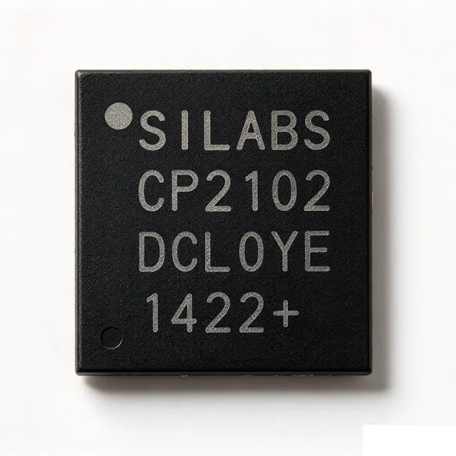
CP2102-GM - USB-to-UART Bridge, QFN-28 | Silicon Laboratories
The Silicon Laboratories CP2102-GM is a highly integrated USB-to-UART Bridge Controller that provides a compact solution for migrating RS-232 designs to USB using a minimum of components and PCB area, packaged in a 5x5 mm 28-pin QFN (QFN-28) with exposed thermal pad. The device integrates a USB 2.0 full-speed function controller, USB transceiver, on-chip oscillator, internal EEPROM, and an asynchronous serial data bus (UART) with full modem control signals, eliminating the need for external USB components. A USB-to-UART bridge controller is a type of bridge IC that sits between a USB host and a legacy UART peripheral, translating USB protocol packets into asynchronous serial bytes and vice versa. In the broader taxonomy, the CP2102-GM belongs to interface ICs (USB bridge controllers), which are a sub-category of communication interface semiconductors that enable protocol translation between modern serial buses and legacy parallel/asynchronous interfaces used in microcontrollers, sensors, and embedded modems. Key features include a 3.0 V to 3.6 V single supply operation, integrated 3.3 V LDO voltage regulator, support for data rates from 300 baud up to 921.6 kbaud, and full modem control signals (RTS, CTS, DTR, DSR, DCD, RI). The internal 1024-byte EEPROM stores customizable product ID, vendor ID, serial number, and GPIO configuration, while royalty-free virtual COM port (VCP) drivers are provided for Windows, macOS, and Linux hosts. The device's architecture combines a USB 2.0 full-speed PHY, an 8051-compatible microcontroller core running the on-chip firmware, and a hardware UART block, with all clock generation handled internally. This integration removes the need for an external crystal, oscillator, or USB termination resistors, dramatically simplifying USB-enabling of legacy microcontroller designs where BOM count is critical. Typical applications include microcontroller-to-USB connectivity on evaluation boards and development kits, industrial point-of-sale terminals, USB dongles for legacy serial equipment, GPS module interfaces, and embedded debug/programming ports. The compact QFN-28 package suits space-constrained PCB layouts where a through-hole DB-9 connector would be impractical. When designing with the CP2102-GM, follow the bus-powered vs self-powered connection diagrams in the Silicon Labs datasheet, since the USB VBUS pin must be routed through a voltage divider when the device is self-powered. Suspend current can be as low as 100 uA, allowing the design to meet USB suspend-current requirements without additional power switching. This page synthesizes distributor pricing, drop-in pin-compatible alternatives, and practical design notes that go beyond what is found in the manufacturer datasheet alone.