메모리 IC
제품 (11)

H5ANAG8NAMR-UHC - 16Gb DDR4-2400 SDRAM 2Gx8 | SK Hynix
The SK Hynix H5ANAG8NAMR-UHC is a 16Gb (2G x 8) DDR4 SDRAM DRAM component operating at DDR4-2400 data rates on a 1.2V supply, housed in a 78-ball FBGA package. It is a Memory IC used for data storage, firmware boot, embedded logging, industrial controllers, computing modules, and replacement sourcing. DDR4 SDRAM (Double Data Rate 4 Synchronous Dynamic Random Access Memory) is the fourth generation of the JEDEC-defined DDR memory family. Within the memory hierarchy, a DRAM component such as this part sits at the main-memory level of a computing system, below CPU caches and above storage. Unlike NAND flash, DRAM is volatile and requires periodic refresh, but delivers far lower random-access latency and high bandwidth, making it the standard main-memory technology from embedded controllers to servers. Key features of the H5ANAG8NAMR-UHC include a 16Gbit density organized as 2G words of 8 bits, a 2400 MT/s interface, and the reduced 1.2V core supply that distinguishes DDR4 from the 1.5V DDR3 generation. DDR4 devices also bring bank-group architecture, which interleaves four internal bank groups to raise effective data rates, plus lower operating currents per transferred bit than previous generations. Technically, this part belongs to SK Hynix DDR4 DRAM component family (the AG8N denotes 16Gb x8 organization within the A-generation die family). Speed grade and voltage class are encoded in the -UHC suffix, which corresponds to DDR4-2400 operation at 1.2V. The 78-ball FBGA (Fine-Pitch Ball Grid Array) lead-free package is the JEDEC-standard footprint shared across most 16Gb x8 DDR4 components, which simplifies second-source qualification. Interface signals include differential clocking (CK/CK#), DQS strobes for data capture, and on-die termination (ODT) to preserve signal integrity at multi-gigabit rates. Typical applications include DRAM modules and DIMMs, industrial controllers and computing modules requiring main memory, networking and communication equipment, and embedded systems performing firmware boot and data logging in volatile memory. The x8 organization suits designs that need many independent chips or ECC-enabled subsystems (8D72 configurations). A key design consideration: DDR4-2400 operation requires careful address/command bus fly-by routing, per-byte DQS trace-length matching, and correct ODT/ZQ calibration in the memory controller configuration. This page synthesizes distributor availability, drop-in alternatives, and practical DDR4 design notes not found in the manufacturer datasheet, giving engineers and buyers a single citable reference.

HMCG84AGBRA191N - 32GB DDR5-5600 ECC RDIMM | SK Hynix
The SK Hynix HMCG84AGBRA191N is a 32GB DDR5-5600 ECC registered DIMM (RDIMM) operating at 1.1V with CL46 latency, 1Rx4 single-rank organization, and a 288-pin DIMM form factor with PC5-44800 bandwidth classification. An RDIMM (Registered DIMM) is a server-class memory module that buffers address and command signals through a registering clock driver (RCD) before they reach the DRAM devices. This buffering reduces electrical loading on the memory controller, allowing servers to populate more DIMM slots per channel than with unbuffered UDIMMs. RDIMMs sit within the memory hierarchy as a type of DDR5 SDRAM module, belonging to the broader category of volatile main-memory components used in computing systems. Key features include DDR5-5600 MT/s data rate for high memory bandwidth, on-die ECC and side-band ECC support for data integrity in servers, a low 1.1V operating voltage that reduces power draw and thermal load compared to DDR4 RDIMMs, and single-rank 1Rx4 organization that maximizes population flexibility on dual-processor server boards. The 288-pin form factor is the standard DDR5 server module connector. Architecturally, DDR5 splits each module into two independent 32-bit subchannels, improving memory access efficiency. On-die ECC corrects internal DRAM cell errors before they reach the bus, while the registered interface and x4 DRAM devices provide robust error containment for enterprise workloads. At 5600 MT/s, the module delivers 44.8 GB/s peak bandwidth per module. Typical applications include edge compute nodes, low-VM-density virtualization hosts, general-purpose rack servers, and enterprise storage controllers where 32GB-per-DIMM density at DDR5-5600 speed is the sweet spot for cost and performance. Design consideration: verify that your server platform, BIOS, and memory controller officially support DDR5-5600 RDIMMs at the target population; many platforms derate speed as DIMMs per channel increase. This page synthesizes distributor pricing, drop-in SK Hynix family alternatives, and practical deployment notes not found in a single manufacturer datasheet.
HUH721010ALE600 - 10TB 7200RPM SATA Enterprise HDD | Western Digital
The Western Digital HUH721010ALE600 (formerly HGST Ultrastar He10) is a 10 TB enterprise-class 3.5-inch SATA hard disk drive spinning at 7200 RPM with a 256 MB cache buffer and SATA 6 Gb/s interface. It belongs to the Ultrastar DC HC510 family and uses conventional Perpendicular Magnetic Recording (PMR) technology rather than shingled recording, making it drop-in compatible with any enterprise SATA backplane. An enterprise hard disk drive is a rotating magnetic storage device engineered for 24/7 operation in data center servers, network-attached storage arrays, and hyperscale object storage. Within the storage hierarchy, HDDs sit beneath SSDs in $/GB but above tape in access latency, occupying the bulk-capacity tier. The HUH721010ALE600 specifically targets the helium-sealed, high-density 10 TB tier with workload ratings suitable for RAID rebuilds and sequential archive workloads. Key differentiating features of this model include a 10 TB raw capacity, a 7200 RPM spindle speed delivering ~225 MB/s sequential throughput, a 256 MB DRAM cache for command queuing, 512e (4K sector) advanced format with 512n emulation, and a helium-filled hermetically sealed enclosure that reduces platter drag and allows 7 platters to be stacked in the standard 26.1 mm z-height. The drive is rated for 550 TB/year workloads and 2.5 million hours MTBF, double that of desktop drives, with a 5-year limited warranty. Architecturally, the HUH721010ALE600 uses a 7-disk, 14-head design with PMR for predictable write performance in RAID arrays. Rotational vibration (RV) sensors maintain throughput when deployed in densely-packed multi-drive chassis. The SATA 6 Gb/s host interface delivers up to 600 MB/s of theoretical bandwidth, ample for the drive's real-world ceiling of ~225 MB/s sequential read. Typical applications include hyperscale object storage, video surveillance NVR arrays with retention over 30 days, cold-data archiving for medical imaging or scientific datasets, mid-range NAS/SAN capacity tiers, and backup targets for virtual machine repositories. The helium platform's power efficiency (typically 6-8 W idle) makes it competitive against 10 TB air-filled drives in 24/7 data center duty cycles. One important design consideration when deploying the HUH721010ALE600 is thermal management. Although helium reduces internal friction, ambient intake temperatures above 40°C shorten component life. Drive bay backplanes should provide at minimum 100 LFM airflow and the host SAS/SATA controller must support 4K native or 512e sectors; legacy 512B-only HBAs require drive firmware reconfiguration or replacement. This page synthesizes distributor pricing, decode-level alternative information, and field-deployment notes not consolidated in the OEM datasheet, supporting procurement and storage architect decisions on 10 TB enterprise helium HDDs.

M29W064FT70N3F - 64Mb 3V NOR Flash 70ns | Micron
The Micron Technology M29W064FT70N3F is a 64-Mbit (64 Mb) 3 V supply parallel NOR Flash memory organized as 8 Mbit x8 or 4 Mbit x16, with a 70 ns access time, housed in a 48-pin TSOP I (12 x 20 mm) package rated from -40C to +125C. Parallel NOR Flash is a nonvolatile memory category that allows random byte-wise access over a parallel address/data bus, making it a subset of Flash memory within the broader memory IC hierarchy (memory IC -> Flash -> NOR Flash -> parallel boot-block NOR). Unlike NAND Flash, NOR devices support execute-in-place (XIP) code storage because every byte is directly addressable, which is why parallel NOR historically serves as boot code memory in embedded systems. Key features of the M29W064FT family include a wide VCC supply range up to 3.6 V for program, erase, and read operations; an optional VPP pin accepting 12 V for accelerated program/erase cycles; page-mode read architecture; and a top boot block organization (the FT suffix) that places the protected boot code blocks at the top of the memory map. The device supports block protection and temporary unprotection for field updates. Technically, the device uses a page read architecture that delivers an initial access time of 70 ns, compatible with zero-wait-state microprocessors. Program and erase operations are managed through a command-set interface compatible with standard JEDEC-style NOR command sets used across the M29W family, and status is monitored via data polling and toggle bits. The industrial temperature rating (-40C to +125C) of the N3F grade suits harsh environments. Typical applications include boot code storage for embedded processors in industrial control, telecommunications and networking line cards, medical instrumentation, and test equipment, where the 70 ns access time supports direct XIP execution without shadow RAM. Designers should note that the 3 V parallel NOR family is largely in lifecycle management; new designs should evaluate Micron SPI NOR (MT25QL/MT25QU) successors, and the top boot block (FT) versus bottom boot block (FB) suffix must match the CPU reset vector mapping. This page synthesizes distributor availability data, same-family drop-in variants, and boot-block selection guidance not found together on the manufacturer datasheet.

M29W128GH70N3E - 128Mb Parallel NOR Flash, 70ns | Micron
The Micron M29W128GH70N3E is a 128Mbit (16MB) parallel NOR flash memory with a 70 ns access time, a 2.7V to 3.6V supply range, and a 56-pin TSOP surface-mount package. Organized as 8M x 16 or 16M x 8, it delivers asynchronous parallel reads suitable for code storage in embedded systems. Parallel NOR flash is a nonvolatile memory technology in which any address can be read directly by presenting the address on a parallel bus, unlike NAND flash which reads in pages through an I/O-multiplexed interface. Within the memory hierarchy, NOR flash sits between DRAM/SRAM (volatile, fast) and mass-storage NAND (dense, block-based), and is the standard choice for storing boot code, firmware images, and parameter tables that the CPU executes or reads in place (XIP). Key features include the 70 ns random-access time supporting zero-wait-state reads from slow buses or cached execution, an automotive temperature grade of -40C to +125C for under-hood and industrial environments, and the widely deployed 56-TSOP footprint inherited from the STMicroelectronics M29W family. Program and erase operations are executed via command-set sequences with status polling, block protection, and a common flash interface for algorithm detection. Technically, the device uses a 3V NOR cell array with internal charge pumps for program/erase high voltages, organized in uniform erase blocks. The 16-bit data bus minimizes glue logic for 16-bit microcontroller and DSP boot flash designs, and the byte/word select pin allows 8-bit systems to reuse the same footprint. Typical applications include automotive ECU boot memory, industrial PLC firmware storage, networking equipment code flash, and set-top-box firmware. The automotive grade and wide bus compatibility make it a natural fit for long-lifecycle embedded platforms. Design consideration: at 70 ns access the part reads comfortably on 50-66 MHz buses with one wait state; for faster systems, verify cycle timing against the datasheet AC table and account for program/erase latency with status polling or interrupts. This page synthesizes distributor pricing, drop-in alternatives, and practical design notes not found in the manufacturer datasheet.
M29W800FB70N3F - 8Mb Parallel NOR Flash 70ns TSOP-48 | Micron
The Micron M29W800FB70N3F is an 8 Mbit (512K x 16 / 1M x 8) 3V parallel NOR Flash memory with 70 ns access time, CFI (Common Flash Interface) programming support, and bottom boot block architecture, housed in a 48-pin TSOP (12 x 20 mm) package. The M29W800FB70N3F is supplied in tape and reel format and is RoHS compliant. A parallel NOR Flash is a non-volatile memory technology that allows random access to any address, making it the classic choice for storing boot code and firmware that a processor executes in place (XIP). Unlike serial NOR or NAND devices, parallel NOR connects directly to a microprocessor address and data bus, which is why it remains popular in industrial controllers, set-top boxes, and automotive electronics where deterministic access time matters more than raw density. Key features include an 8 Mbit density organized as 19 memory blocks (1 boot block, 3 parameter blocks, and 15 main blocks), dual x8/x16 bus organization selected via the BYTE# pin, and a guaranteed 70 ns access time at VCC of 3.0V to 3.6V. The device operates from a single 3V supply for read, program, and erase operations. The device embeds an on-chip program/erase controller executing automatic byte/word program and block erase algorithms, freeing the host CPU from timing management. Typical programming time is 10 microseconds per byte/word. Erase suspend and resume modes allow the CPU to read or program another block while a slow erase cycle is in progress, and an unlock bypass program command accelerates batch programming in production. The RP# (reset/power-down) pin provides instant reset and low standby current. The bottom boot block variant places the 16 Kbyte boot sector at the bottom of the address map, matching processors that keep reset vectors at address 0. Automotive-qualified supply options (per Mouser listing) suit instrument clusters and body electronics. Typical applications include boot firmware storage in set-top boxes, industrial PLCs, networking equipment, and automotive modules requiring a 3V parallel boot Flash. Design consideration: verify boot block location (bottom vs. top) against the processor reset vector map before committing the layout; the FT (top boot) variant is the pin-compatible complement. This page synthesizes distributor pricing, drop-in alternatives, and practical design notes not found in the manufacturer datasheet.

MT40A1G16TB-062E-ITF - 16Gb DDR4 SDRAM x16 96-FBGA | Micron
The Micron Technology MT40A1G16TB-062E IT:F is a 16Gbit DDR4 SDRAM memory IC organized as 1G x 16, operating with a 1.6 GHz clock (DDR4-3200 class timing, 19 ns access) in a 96-ball FBGA package measuring 7.5 mm x 13 mm. The IT:F suffix indicates an industrial operating temperature range of -40C to +95C with a lead-free, RoHS-compliant finish, making it suited for harsh-environment embedded designs. DDR4 SDRAM (Double Data Rate 4 Synchronous Dynamic Random Access Memory) is the fourth generation of the JEDEC-defined DDR memory family used as main memory across servers, networking, industrial automation, and high-performance embedded systems. Within the memory hierarchy, it sits as a high-density volatile working memory between the CPU cache and non-volatile storage, offering far higher density and bandwidth than DDR3 while reducing operating voltage and power per transfer. Key features include 16Gbit density in a single x16 component, an internal bank-group architecture that accelerates random-access performance versus conventional DDR4 bank arrangements, and the 062 speed grade supporting 1.6 GHz operation. Micron implements auto self-refresh, auto precharge, write leveling, data mask, dynamic on-die termination (ODT), and CRC/data bus inversion functions per the DDR4 standard. Technically, the device uses a 1.2 V core supply typical of the DDR4 generation, with on-die termination, programmable CAS latency, and refresh management (including self-refresh and temperature-compensated refresh) handled by an internal mode-register set configured at initialization. The 96-FBGA ball map follows the standard JEDEC x16 DDR4 footprint, enabling second-source qualification on existing land patterns. Typical applications include industrial controllers and edge-computing gateways, networking line cards and switch fabrics, test and measurement instruments, and embedded vision or AI acceleration modules that require gigabyte-class working memory over an industrial temperature range. A key design consideration: DDR4 signal integrity demands length-matched, impedance-controlled routing (typically 40 ohm ODT settings and fly-by or tee topologies) plus careful VREF and power-plane decoupling; verify controller compatibility with the 062 speed grade timing before layout freeze. This page synthesizes distributor pricing, drop-in alternatives, and practical design notes not found in the manufacturer datasheet, with data verified against DigiKey, Mouser, Octopart, and Micron product pages as of 2026-09-27.
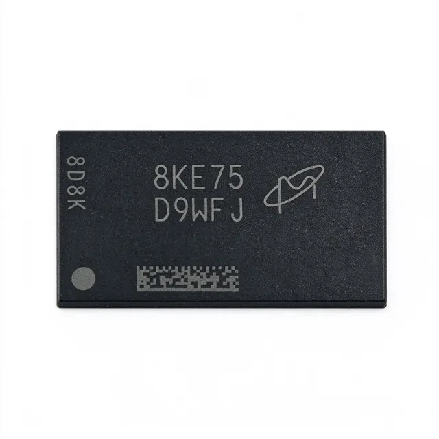
MT40A512M16LY-062E - 8Gb DDR4 SDRAM 3200MT/s | Micron
The Micron Technology MT40A512M16LY-062E is an 8Gb DDR4 SDRAM organized as 512M x 16, operating at the DDR4-3200 speed grade (1.6 GHz clock, 3200 MT/s data rate) in a 96-ball FBGA package measuring 7.5 x 13.5 mm. DDR4 SDRAM (fourth-generation Double Data Rate Synchronous Dynamic Random-Access Memory) is a volatile memory that transfers data on both edges of the clock, doubling effective data rate versus SDR DRAM. Within the memory hierarchy it sits as the main-system-memory class of DRAM, below caches and above storage, and succeeds DDR3 with lower operating voltage and higher densities. DDR4 runs its core and I/O at VDD = VDDQ = 1.2V +/- 60mV, down from DDR3's 1.5V, cutting dynamic power while enabling higher speeds and per-device capacity up to 16Gb. Key features of this device include 16 internal banks grouped in 2 bank groups of 4 (x16 configuration), on-die internal adjustable VREFDQ generation that simplifies memory-controller design, and 1.2V pseudo open-drain I/O. The IT industrial temperature grade supports a refresh window of 8192 cycles at 64ms for -40C to +85C, 32ms for >85C to +95C, and 16ms beyond 95C. VPP is supplied at 2.5V (-125mV/+250mV) exclusively for cell bootstrap pumping. Advanced capability set includes auto self-refresh, write leveling, dynamic on-chip termination (ODT), CRC and CA parity support, data mask, auto precharge, asynchronous reset, and ZQ calibration via an external 240-ohm reference resistor. Typical applications are industrial embedded controllers, networking equipment line cards, and high-performance computing or data-center memory subsystems where 3200 MT/s bandwidth per device and industrial temperature range are required. Design-wise, plan controlled-impedance fly-by routing, 1.2V and 2.5V rails with adequate decoupling, and connect the ZQ ball to ground through exactly 240 ohms; the controller must support 2tCK ODT updates at this speed grade. This page adds distributor pricing tiers, drop-in alternatives across Micron, Nanya, Samsung, and SK hynix, plus practical DDR4 design notes not found in the manufacturer datasheet alone.
MT53B128M32D1DS-062 - 4Gbit LPDDR4 SDRAM 1.6GHz | Micron
The Micron Technology MT53B128M32D1DS-062 is a 4Gbit mobile LPDDR4 SDRAM memory IC organized as 128M x 32, operating at 1600 MHz (DDR-3200 data rate) from a 1.1V core supply, housed in a 200-ball WFBGA (10 x 14.5 mm) package. LPDDR4 (Low Power Double Data Rate 4) is a JEDEC-defined synchronous DRAM interface standard optimized for mobile and battery-powered systems. Compared with standard DDR4 SDRAM, LPDDR4 lowers the core voltage to 1.1V, uses a point-to-point channel architecture, and introduces features such as deep power-down, per-bank refresh, and low-power idle states that reduce standby current. In the memory hierarchy, it sits within the SDRAM family of volatile semiconductor memories, falling under the broader categories of DRAM and memory ICs. Key features of this device include the 4Gbit density in a x32-wide organization that simplifies 32-bit bus designs, the -062 speed grade supporting a 1600 MHz clock for high memory bandwidth, and a compact 200-ball fine-pitch BGA footprint suited to space-constrained boards. Micron speed-grade and temperature suffixes define operating ranges across commercial and industrial conditions. Architecturally, the die implements LPDDR4 bank groups, burst lengths of 8 and 16, and programmable refresh schemes that balance bandwidth against power. The 1.1V VDD core, combined with VDDQ I/O termination optimization, minimizes dynamic power during burst transfers, while DPD (deep power down) allows microamp-level standby in always-on mobile designs. Typical applications include smartphone and tablet application-processor memory, embedded Linux gateways and routers, automotive infotainment and ADAS compute modules (using the AUT variant), and industrial edge-AI vision modules where 4Gbit capacity and LPDDR4 bandwidth are required. Design consideration: LPDDR4 requires careful length-matched routing and controller training for read/write leveling; verify the controller supports x32 LPDDR4 and confirm the speed-grade suffix matches your thermal environment before finalizing the BOM. This page synthesizes distributor pricing, same-family drop-in variants, and practical design notes not found in the manufacturer datasheet. Pricing references are as of 2026-09-02.
MTFDKCC15T3TGH-1BC1ZABYY - 15.36TB 9400 PRO NVMe U.3 SSD
The Micron MTFDKCC15T3TGH-1BC1ZABYY is a 9400 PRO 15.36 TB enterprise NVMe solid-state drive in the U.3 (15 mm) 2.5-inch form factor, with a PCIe Gen4 x4 host interface and TLC 3D NAND. It is part of Micron's data-center SSD portfolio tuned for read-intensive workloads at 1 DWPD endurance. An enterprise NVMe SSD is a high-performance non-volatile storage device that connects to the host system via the Non-Volatile Memory Express protocol over a PCIe physical layer, bypassing legacy SAS/SATA controller overhead. Within the broader storage hierarchy, NVMe SSDs sit between DRAM (volatile, fastest) and SATA SSDs/HDDs (slower, larger capacity), and they are categorized as data-center SSDs (DC SSDs) when qualified for 24/7 mixed-workload server operation. The 9400 PRO family specifically targets read-intensive, capacity-dense workloads such as object stores, content delivery, and large-scale analytics. Key features of the MTFDKCC15T3TGH-1BC1ZABYY include a usable capacity of 15.36 TB, PCIe Gen4 NVMe 1.4 interface, sequential read performance up to 7,000 MB/s and sequential write up to 7,000 MB/s (class-leading for capacity), random 4 KB read up to 1.1M IOPS, and 1 DWPD endurance rated for five years. The drive uses Micron's 176-layer TLC NAND and ships in the 70 x 100 x 15 mm U.3 (SFF-TA-1001) hot-swap form factor, supporting U.3 backplane interoperability with U.2 hosts via adapter. Architecturally, the 9400 PRO leverages a multi-core NVMe controller with hardware-accelerated LDPC ECC, end-to-end data-path protection (PLP), and dynamic namespace management. PCIe Gen4 doubles per-lane throughput versus Gen3, and combined with 16 NAND channels this unlocks the dual 7 GB/s read/write figure. AES-256 hardware encryption, TCG Opal 2.0 (where ordered), Sanitize and Format NVM commands, and power-loss protection make it suitable for enterprise security and compliance frameworks. Typical applications include hyperscale object storage (Ceph, S3-compatible), AI/ML training data lakes, video streaming and CDN edge caches, database warehousing, VMware vSAN capacity tiers, and read-heavy analytics workloads. The 1 DWPD rating means it is best fitted to read-dominated rather than write-heavy log or database primary storage. When designing with this drive, ensure the host backplane supports the U.3 (SFF-TA-1001) connector; legacy U.2 (SFF-8639) backplanes remain compatible via dual-mode pinout. Confirm platform BIOS/UEFI NVMe driver support and thermal envelope (typically up to 25 W active) - server front-panel airflow above 1.5 m/s is recommended at full load. This page synthesizes distributor pricing, drop-in alternatives drawn from the verified web cross-reference, and practical design notes for data-center SSD selection not found in a single datasheet.
MZ7WD480HCGM-00003 - Samsung SM843TN 480GB SATA SSD | 2.5" Enterprise
The Samsung MZ7WD480HCGM-00003 is the Samsung SM843TN enterprise-grade 2.5" SATA III (6 Gb/s) solid-state drive with a 480 GB capacity, utilizing Samsung's 20 nm MLC NAND flash and a proprietary Samsung controller. It is engineered for read-intensive data-center workloads, delivering sequential read performance up to 530 MB/s and sequential write performance up to 360 MB/s, with a 7 mm z-height that fits standard 2.5" server bays. A solid-state drive (SSD) is a data storage device that uses non-volatile flash memory (typically NAND) to persist data, replacing rotating hard disk drives (HDDs). SSDs sit in the storage hierarchy between DRAM caches and HDDs, offering orders-of-magnitude lower latency and much higher IOPS per watt. Enterprise SATA SSDs occupy the mainstream product-tier performance slot, balancing cost per GB against throughput and endurance; they fall under the broader category of NAND flash storage -> persistent memory -> data storage device -> computer hardware. Key specifications include 1.8 DWPD (drive writes per day) endurance rating over a 5-year warranty period, SED (Self-Encrypting Drive) support via TCG-Enterprise, power-loss data protection through onboard tantalum capacitors, and a sustained random 4 KB read IOPS figure suited for online transaction processing and virtual-desktop infrastructure (VDI) boot storms. The drive conforms to the SATA 3.2 specification and supports ATA-8 ACS command set, SMART monitoring, and NCQ (Native Command Queuing). The SM843TN architecture pairs Samsung's PX-series enterprise controller with MLC NAND and a DRAM cache buffer, achieving predictable latency under mixed read/write workloads typical of read-intensive applications. Power-loss protection circuitry uses the energy stored in capacitors to flush the in-flight write cache to NAND, preventing data corruption during unexpected power events — a critical feature for database and virtualization tiers. Typical deployment scenarios include read-intensive database servers, VDI boot images, content delivery network (CDN) edge caches, web-server front-end tiers, and email/messaging archive storage where sequential read throughput, predictable latency, and SED security outweigh the need for high write endurance. The 480 GB capacity is well-matched to boot partitions, indexing databases, and per-VM virtual-disk provisioning. When integrating this drive, verify that the host backplane supports SATA 6 Gb/s (SATA III) to achieve the rated 530 MB/s sequential read speed; legacy SATA II (3 Gb/s) hosts will throttle sequential throughput. For RAID arrays, match with other SM843T/SM843TN drives of identical firmware to avoid compatibility warnings on enterprise controllers (LSI/Broadcom, MegaRAID).