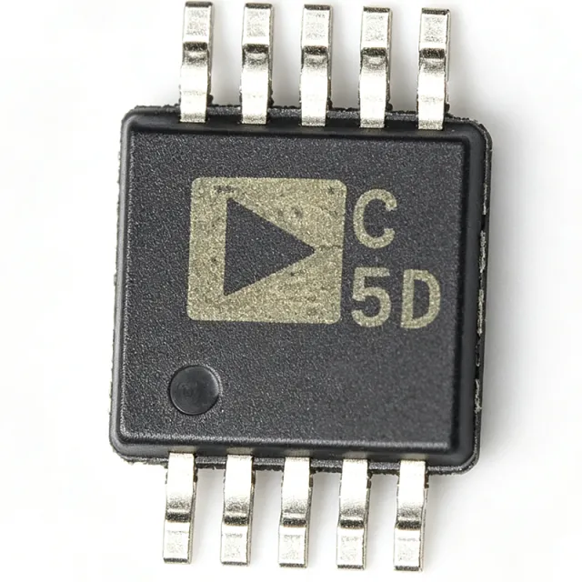
AD7980BRMZRL7 - 16-Bit 1 MSPS PulSAR ADC | Analog Devices
부품 번호: AD7980BRMZRL7 ✓ 활성| 수량 | 단가 | 합계 |
|---|---|---|
| 1 | $16.25 | $16.25 |
| 10 | $14.62 | $146.20 |
| 100 | $12.98 | $1,298.00 |
| 500 | $11.84 | $5,920.00 |
| 1,000 | $10.75 | $10,750.00 |
AD7980BRMZRL7 개요
What is a SAR ADC? A Successive Approximation Register ADC is a class of analog-to-digital converter that uses a binary search algorithm together with a charge-redistribution DAC to step toward the digital representation of the input voltage one bit per clock cycle. SAR ADCs are valued for their deterministic behavior, zero pipeline latency, low power consumption, and excellent DC linearity, and they occupy the role of mid-speed precision converter within the broader hierarchy: SAR ADC -> ADC -> data converter -> mixed-signal IC -> semiconductor.
Key features of the AD7980BRMZRL7 include ±0.6 LSB typical INL (1.25 LSB max), 91.5 dB SNR and 92 dB dynamic range at VREF = 5 V, an SPI-compatible serial port that supports daisy-chaining multiple ADCs on a 3-wire bus via the SDI input, and an optional BUSY indicator. The digital I/O is compatible with 1.8 V to 5 V logic families, allowing direct connection to modern MCUs and FPGAs without level shifters.
The AD7980 uses a low-noise, fully differential charge-redistribution DAC core combined with a precision comparator and SAR logic, achieving 16-bit resolution while consuming only a few milliwatts at full 1 MSPS throughput. Power consumption scales linearly with sample rate, enabling sub-mW operation when the part is clocked down for battery-powered or thermal-sensitive designs. The 10-lead MSOP footprint measures approximately 3 mm x 3 mm, making the part suitable for dense, multi-channel data-acquisition boards.
Typical applications include precision industrial process control loops, portable medical instrumentation, multi-channel data-acquisition modules, optical networking feedback loops, and battery-powered measurement front ends. The combination of 1 MSPS throughput, low power, and small footprint makes it ideal for distributed sensing nodes and high-density plug-in cards.
When designing with the AD7980, drive the analog input with a low-impedance buffer to minimize kickback and aperture uncertainty, decouple VREF with high-quality ceramic capacitance, and route the serial lines with short, impedance-controlled traces to preserve acquisition timing margins.
This page synthesizes distributor pricing as of 2026-10-06, drop-in same-package alternatives sourced from Analog Devices' own PulSAR family, and practical design notes not aggregated on any single distributor page.
드롭인 대체품: AD7980BRMZRL7 — 동일 패키지, 핀 호환. PCB 재작업이 필요한 다른 패키지 부품은 제외됩니다.
이 시리즈의 변형
다음과 드롭인 호환되는 동일 시리즈 모델: AD7980BRMZRL7 (동일 폼 팩터 및 풋프린트) — 차이점: Architecture, Package, RoHS Status, Resolution, Input Type.
빠른 비교 도구 — 나란히 비교할 대체 부품을 선택하십시오:
AD7982BRMZ
✅ 드롭인📋 참조 대체품 (카탈로그에 없음)
AD7982BRMZRL7
✅ 드롭인📋 참조 대체품 (카탈로그에 없음)
AD7988-5BRMZ
✅ 드롭인📋 참조 대체품 (카탈로그에 없음)
AD7988-5BRMZRL7
✅ 드롭인📋 참조 대체품 (카탈로그에 없음)
AD7690BRMZ
✅ 드롭인✓ 재고 있음
$17.6 / 개
데이터시트 보기 →AD7980BRMZ
✅ 드롭인✓ 재고 있음
$16.8636 / 개
데이터시트 보기 →AD7980BRMZRL7 최대 정격 & 전기적 특성
| 분해능 | 16 bits |
| Architecture | SAR (Successive Approximation Register) |
| 샘플링 속도 | 1 MSPS |
| Number of Channels | 1 |
| Analog Input Type | Pseudo-differential (0 V to VREF) |
| Reference Voltage Range (VREF) | 2.5 V to 5 V |
| Supply Voltage (VDD) | 2.5 V to 5.5 V |
| Digital I/O Logic Compatibility | 1.8 V to 5 V |
| INL (typical / max) | ±0.6 LSB / ±1.25 LSB |
| SNR (fIN = 10 kHz, VREF = 5 V) | 91.5 dB |
| Dynamic Range (VREF = 5 V) | 92 dB |
| Missing Codes | None (16-bit, no missing codes guaranteed) |
| Latency | Zero latency |
| Serial Interface | SPI-compatible, 3-wire, daisy-chainable |
| 패키지 | 10-lead MSOP (RM) |
| 실장 유형 | Surface Mount |
| 동작 온도 | -40C to +85C |
| Reel Size | 7-inch (RL7 suffix) |
| RoHS 상태 | ROHS3 Compliant |
| REACH Status | REACH Unaffected |
| MSL 레벨 | MSL 1 (Unlimited) |
AD7980BRMZRL7 핀 구성
| 핀 1 | VDD — Power supply input (2.5 V to 5.5 V) |
| 핀 2 | GND — Ground reference |
| 핀 3 | REF — External reference voltage input (2.5 V to 5 V) |
| 핀 4 | IN+ — Analog input positive (pseudo-differential) |
| 핀 5 | IN- — Analog input negative (tie to GND for single-ended) |
| 핀 6 | GND — Ground reference |
| 핀 7 | SDI — Serial data input (daisy-chain mode) |
| 핀 8 | SDO — Serial data output |
| 핀 9 | SCK — Serial clock input |
| 핀 10 | CNV — Convert input (initiates conversion on rising edge) |
일반적인 애플리케이션
AD7980BRMZRL7 적합 용도: 6 애플리케이션s: Precision Industrial Process Control, Portable Medical Instrumentation, Multi-Channel Data Acquisition Modules, Optical Networking Feedback Loops, Battery-Powered Measurement Front End, Programmable Logic Controller (PLC) Analog Input Cards.
Precision Industrial Process Control
The AD7980BRMZRL7 fits precision industrial process-control loops because its 16-bit resolution, ±0.6 LSB typical INL, and 91.5 dB SNR at VREF = 5 V deliver accurate measurement of 4-20 mA-derived signals, thermocouple amplifiers, and strain-gauge bridges. The 1 MSPS throughput allows simultaneous sampling of multiple multiplexed channels when paired with an external MUX, and the 10-lead MSOP package enables dense, multi-channel plug-in cards. Its 2.5 V to 5.5 V VDD supply aligns with common 3.3 V and 5 V industrial rails, while the SPI-compatible daisy-chain interface reduces FPGA pin count when several ADCs share a single bus. Power consumption scales linearly with sample rate, simplifying thermal budgeting in enclosed DIN-rail enclosures.
추천
Portable Medical Instrumentation
The AD7980BRMZRL7 is ideal for portable medical instrumentation where 16-bit precision and low power are both required. Its SAR architecture delivers zero-latency conversion critical for paced ECG and pulse-oximeter front ends, while the 92 dB dynamic range preserves the small-amplitude bioelectric signals above the noise floor. The 10-lead MSOP footprint occupies roughly 9 mm² of PCB area, allowing wrist-worn patient monitors and bedside telemetry units to integrate multi-lead front ends without board bloat. Power scales linearly with throughput, so dropping the sample rate to 100 kSPS reduces dissipation into the sub-mW range suitable for AAA-battery-powered devices. The SPI interface connects directly to ARM Cortex-M MCUs without level shifters.
추천
Multi-Channel Data Acquisition Modules
The AD7980BRMZRL7 suits multi-channel data-acquisition modules where high channel density and deterministic sampling matter. Its SPI-compatible serial interface supports daisy-chaining multiple ADCs on a single 3-wire bus, allowing a single FPGA or MCU SPI master to manage 8, 16, or more channels without dedicating a chip-select line per converter. The 1 MSPS per-channel throughput supports simultaneous-sampling architectures when paired with external track-and-hold or per-channel MUX schemes. The 10-lead MSOP package keeps each ADC channel compact, and the 1.8 V to 5 V digital I/O range allows the part to interface directly to 1.8 V FPGAs and 5 V MCUs equally well. Reference decoupling requirements are modest: 10 µF plus 100 nF ceramic typically achieves full performance.
추천
Optical Networking Feedback Loops
The AD7980BRMZRL7 is well suited to optical networking feedback loops that monitor laser driver currents and photodiode return signals. Its 1 MSPS sampling rate is fast enough to capture modulation envelopes in 10G transponder control loops, and the 91.5 dB SNR preserves the dynamic range needed for accurate average-power measurements across temperature. The pseudo-differential 0 V to VREF input accepts directly-coupled photodiode transimpedance outputs, simplifying the analog front end. The 10-lead MSOP package tolerates the reflow profiles required for optical transceiver PCB assembly, and the part's 2.5 V to 5.5 V supply matches the common 3.3 V transceiver rails. Daisy-chaining via SDI allows multiple ADCs to share a single FPGA SERDES link.
추천
Battery-Powered Measurement Front End
The AD7980BRMZRL7 is ideal for battery-powered measurement front ends such as handheld multimeters, environmental loggers, and field-portable test instruments. Power dissipation scales linearly with throughput, so clocking the part at 10 kSPS reduces drain to a few hundred microwatts, extending coin-cell runtime into the multi-year range. The 1.8 V to 5 V digital I/O allows direct connection to modern low-power MCUs without additional regulators, reducing the bill of materials. The 91.5 dB SNR at VREF = 5 V gives 16-bit effective resolution for transducer signals, while the small 10-lead MSOP footprint fits inside sealed probe housings. The pseudo-differential input accepts sensor bridges and thermocouples without instrumentation amplifiers.
추천
Programmable Logic Controller (PLC) Analog Input Cards
The AD7980BRMZRL7 fits PLC analog input cards that digitize 0-10 V or 4-20 mA field signals. Its pseudo-differential input and 2.5 V to 5 V external reference simplify scaling with on-board rail voltages, while the 1 MSPS throughput enables oversampling for 50 Hz / 60 Hz line-noise rejection at decimated rates. The 10-lead MSOP package supports dense 8-channel or 16-channel analog cards that drop into standard PLC backplanes. SPI daisy-chaining reduces FPGA pin usage, leaving more logic available for IEC 61131-3 runtime and communication stacks. The industrial -40C to +85C operating range covers unheated cabinet environments, and the MSL-1 unlimited rating simplifies field-replacement logistics.
추천
추천 제품 요약
엔지니어링 참조 데이터: AD7980BRMZRL7 — 비교, 설계 지침 및 규정 준수 정보.
선택 가이드
대체품과의 비교
| 파라미터 | 이 제품 | AD7982BRMZ | AD7982BRMZRL7 | AD7988-5BRMZ | AD7988-5BRMZRL7 | AD7690BRMZ | AD7980BRMZ |
|---|---|---|---|---|---|---|---|
| Brand | Analog Devices | Analog Devices | Analog Devices | Analog Devices | Analog Devices | Analog Devices | Analog Devices |
| Package | MSOP-10 (RM) | MSOP-10 (RM) - same | MSOP-10 (RM) - same | MSOP-10 (RM) - same | MSOP-10 (RM) - same | MSOP-10 (RM) - same | MSOP-10 (RM) - same |
| Resolution | 16 bits | 18 bits | 18 bits | 16 bits | 16 bits | 18 bits | 16 bits |
| Sampling Rate | 1 MSPS | 1 MSPS | 1 MSPS | 500 kSPS | 500 kSPS | 400 kSPS | 1 MSPS |
| Architecture | SAR (PulSAR) | SAR (PulSAR) | SAR (PulSAR) | SAR (PulSAR) | SAR (PulSAR) | SAR (PulSAR) | SAR (PulSAR) |
| Analog Input Type | Pseudo-differential | Pseudo-differential | Pseudo-differential | Pseudo-differential | Pseudo-differential | Pseudo-differential | Pseudo-differential |
| Supply Voltage | 2.5 V to 5.5 V | 2.5 V to 5.5 V | 2.5 V to 5.5 V | 2.5 V to 5.5 V | 2.5 V to 5.5 V | 2.5 V to 5.5 V | 2.5 V to 5.5 V |
| Digital Logic Compatibility | 1.8 V to 5 V | 1.8 V to 5 V | 1.8 V to 5 V | 1.8 V to 5 V | 1.8 V to 5 V | 1.8 V to 5 V | 1.8 V to 5 V |
| Reel/Packaging Variant | Tape & Reel, 7-inch (-RL7) | Tube | Tape & Reel, 7-inch | Tube | Tape & Reel, 7-inch | Tube | Tube |
주요 차별점
- 1 MSPS full throughput with zero latency (vs AD7690BRMZ)
- Pin-for-pin compatible 18-bit upgrade path (vs AD7982BRMZ)
- Highest full-rate throughput in 16-bit PulSAR family (vs AD7988-5BRMZ)
- Wide 1.8 V to 5 V digital logic compatibility (vs AD7982BRMZRL7)
설계 노트
The AD7980BRMZRL7 power dissipation scales linearly with sample rate. At 1 MSPS the part typically consumes approximately 7 mW from a 5 V supply, while dropping to 100 kSPS reduces dissipation into the sub-mW range. Estimated: at VDD = 5 V, IDD scales at roughly 1.4 mA per MSPS; for battery-powered designs, clock the part only while acquiring to extend runtime. The MSOP-10 thermal resistance of approximately 200 C/W (theta_JA) is more than adequate at these power levels and requires no external copper heat sinking.
Decouple VDD and REF pins with a 10 µF ceramic capacitor in parallel with a 100 nF X7R capacitor placed within 3 mm of the package pins, per the Analog Devices evaluation board layout. Use a solid unbroken ground plane beneath the ADC, and keep analog (IN+, IN-, REF) traces short and isolated from the digital SPI lines (CNV, SCK, SDO, SDI, BUSY). Route the reference input with a guard trace tied to ground to reduce noise injection. For multi-channel boards, place a dedicated ferrite bead on the analog supply rail to isolate the ADC from digital switching transients.
Do not exceed the maximum VREF of 5 V or the absolute maximum analog input range of -0.3 V to VREF + 0.3 V, or the input ESD structures will forward-bias and degrade linearity. The IN- pin must be tied to local analog ground (not the noisy digital ground) when using single-ended inputs, or pseudo-differential common-mode rejection will collapse. When daisy-chaining multiple ADCs, ensure the last device in the chain has SDI tied to logic-low so the SDO output stays enabled. Finally, do not leave CNV floating during power-down, or the next conversion may trigger spuriously.
Drive the analog input through a low-impedance buffer (such as an ADA4841 or AD8021 op-amp) to minimize ADC input kickback and aperture uncertainty. Estimated: the AD7980BRMZRL7 input presents a switched load of approximately 30 pF that is sampled once per conversion; without a buffer, source impedances above 200 ohm can degrade THD. Keep SCK traces short and series-terminate if the cable length exceeds approximately 50 mm, or ground-bounce from the digital return currents can couple back into the analog reference and degrade SNR.
규정 준수 정보
ROHS3 Compliant and REACH Unaffected per PartGenie component data. MSL 1 (Unlimited) rating simplifies field-replacement logistics. Not AEC-Q100 qualified - choose AD7980 automotive-grade variant for automotive applications.







