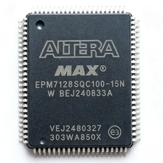
EPM7128SQC100-15 - MAX 7000 CPLD 128MC 15ns 5V | Altera/Intel
부품 번호: EPM7128SQC100-15 ⚠ 최종 구매| 수량 | 단가 | 합계 |
|---|---|---|
| 1 | $14.5 | $14.50 |
| 10 | $12.85 | $128.50 |
| 100 | $10.95 | $1,095.00 |
| 500 | $9.4 | $4,700.00 |
| 1,000 | $8.2 | $8,200.00 |
EPM7128SQC100-15 개요
A CPLD (Complex Programmable Logic Device) is a non-volatile programmable logic IC that combines multiple PAL-like macrocell arrays on a single die with a global interconnect fabric. The MAX 7000 family is Altera's second-generation EEPROM-based CPLD architecture, positioned between simple PLDs and FPGAs in the programmable logic hierarchy: PLD -> CPLD -> FPGA -> SoC FPGA. MAX 7000 parts retain configuration in on-chip EEPROM, so they boot instantly at power-up without an external configuration PROM - an advantage over SRAM-based FPGAs in deterministic-startup applications.
Key features of the EPM7128SQC100-15 include 128 macrocells organized into 4 Logic Array Blocks (LABs), a 2,500-gate typical density, 84 user I/O pins, programmable power management with macrocell-level slew-rate control, and a 15 ns tPD (worst-case pin-to-pin delay) suitable for 66 MHz operation. The device also provides 4 dedicated inputs, 6 to 10 product terms per macrocell, and a JTAG boundary-scan test interface compliant with IEEE 1149.1.
The architecture uses Altera's classic MAX (Multiple Array matriX) interconnect, with each LAB containing 16 macrocells feeding a Programmable Interconnect Array (PIA). This structure delivers fast, predictable combinational and registered logic delays that are independent of routing density - a key reason MAX 7000 CPLDs remain in long-life programs where deterministic timing matters more than raw density.
Typical applications include bus-interface glue logic, peripheral decoders and address mapping, state-machine control in industrial automation, board-level signal conditioning in telecom backplanes, and pin-compatible upgrades for legacy 5 V TTL/CMOS designs. The 5 V tolerance and PQFP-100 footprint also make it a common choice for maintenance of installed equipment in factory automation and aerospace ground systems.
When designing with this part, plan for an external 5 V regulator with at least 200 mA headroom and follow Altera's JTAG chain layout guidelines (TCK pull-down, TMS/TDI pull-ups) to avoid programming failures. Note that the EPM7128SQC100-15 is a mature / legacy product; verify lifecycle status before new designs.
This page synthesizes distributor pricing, drop-in same-package alternatives from the MAX 7000 / MAX 7000A families, and practical design notes not found in the manufacturer datasheet itself.
드롭인 대체품: EPM7128SQC100-15 — 동일 패키지, 핀 호환. PCB 재작업이 필요한 다른 패키지 부품은 제외됩니다.
이 시리즈의 변형
다음과 드롭인 호환되는 동일 시리즈 모델: EPM7128SQC100-15 (동일 폼 팩터 및 풋프린트) — 차이점: Package, Operating Temperature, Propagation Delay (tPD), RoHS Status, Usable Gates.
빠른 비교 도구 — 나란히 비교할 대체 부품을 선택하십시오:
EPM7128SQC100-10
✓ 재고 있음
$9.85 / 개
데이터시트 보기 →EPM7128SQC100-10N
✓ 재고 있음
$14.95 / 개
데이터시트 보기 →EPM7128EQC100-10
✓ 재고 있음
$9.85 / 개
데이터시트 보기 →EPM7128BTC100-10
✓ 재고 있음
$11.2 / 개
데이터시트 보기 →EPM7128SQC100-15N
📋 참조 대체품 (카탈로그에 없음)
EPM7128SQC100-15FN
📋 참조 대체품 (카탈로그에 없음)
EPM7128EQC100-15
📋 참조 대체품 (카탈로그에 없음)
EPM7128SQC100-15 최대 정격 & 전기적 특성
| Family | MAX 7000 |
| Device Type | CPLD (Complex Programmable Logic Device) |
| Macrocells | 128 |
| Logic Array Blocks (LABs) | 4 (16 macrocells each) |
| User I/Os | 84 |
| Pin-to-Pin Delay (tPD) | 15 ns |
| Typical Gate Count | 2,500 gates |
| Supply Voltage (VCCINT) | 5 V (5% tolerance) |
| Programming Technology | EEPROM (in-system programmable via JTAG) |
| JTAG Interface | IEEE Std. 1149.1 compliant |
| 패키지 | 100-pin PQFP (Plastic Quad Flat Pack) |
| 동작 온도 | 0C to +70C (Commercial) |
| 실장 유형 | Surface Mount |
| MSL 레벨 | 3 (168 hours) |
| RoHS 상태 | Non-compliant (SnPb lead finish - legacy PQFP) |
EPM7128SQC100-15 핀 구성
| 핀 1 | I/O — User I/O pin (macrocell-driven bidirectional) |
| 핀 2 | I/O — User I/O pin |
| 핀 3 | I/O — User I/O pin |
| 핀 4 | I/O — User I/O pin |
| 핀 5 | I/O — User I/O pin |
| 핀 6 | I/O — User I/O pin |
| 핀 7 | I/O — User I/O pin |
| 핀 8 | I/O — User I/O pin |
| 핀 9 | I/O — User I/O pin |
| 핀 10 | I/O — User I/O pin |
| 핀 11 | GND — Ground |
| 핀 12 | I/O — User I/O pin |
| 핀 13 | I/O — User I/O pin |
| 핀 14 | I/O — User I/O pin |
| 핀 15 | I/O — User I/O pin |
| 핀 16 | I/O — User I/O pin |
| 핀 17 | I/O — User I/O pin |
| 핀 18 | I/O — User I/O pin |
| 핀 19 | I/O — User I/O pin |
| 핀 20 | I/O — User I/O pin |
| 핀 21 | GND — Ground |
| 핀 22 | I/O — User I/O pin |
| 핀 23 | I/O — User I/O pin |
| 핀 24 | I/O — User I/O pin |
| 핀 25 | I/O — User I/O pin |
| 핀 26 | I/O — User I/O pin |
| 핀 27 | I/O — User I/O pin |
| 핀 28 | I/O — User I/O pin |
| 핀 29 | I/O — User I/O pin |
| 핀 30 | I/O — User I/O pin |
| 핀 31 | GND — Ground |
| 핀 32 | I/O — User I/O pin |
| 핀 33 | I/O — User I/O pin |
| 핀 34 | I/O — User I/O pin |
| 핀 35 | I/O — User I/O pin |
| 핀 36 | I/O — User I/O pin |
| 핀 37 | I/O — User I/O pin |
| 핀 38 | I/O — User I/O pin |
| 핀 39 | I/O — User I/O pin |
| 핀 40 | I/O — User I/O pin |
| 핀 41 | GND — Ground |
| 핀 42 | I/O — User I/O pin |
| 핀 43 | I/O — User I/O pin |
| 핀 44 | I/O — User I/O pin |
| 핀 45 | I/O — User I/O pin |
| 핀 46 | I/O — User I/O pin |
| 핀 47 | I/O — User I/O pin |
| 핀 48 | I/O — User I/O pin |
| 핀 49 | I/O — User I/O pin |
| 핀 50 | I/O — User I/O pin |
| 핀 51 | GND — Ground |
| 핀 52 | I/O — User I/O pin |
| 핀 53 | I/O — User I/O pin |
| 핀 54 | I/O — User I/O pin |
| 핀 55 | I/O — User I/O pin |
| 핀 56 | I/O — User I/O pin |
| 핀 57 | I/O — User I/O pin |
| 핀 58 | I/O — User I/O pin |
| 핀 59 | I/O — User I/O pin |
| 핀 60 | I/O — User I/O pin |
| 핀 61 | GND — Ground |
| 핀 62 | TDI — JTAG Test Data In |
| 핀 63 | TMS — JTAG Test Mode Select |
| 핀 64 | TCK — JTAG Test Clock |
| 핀 65 | VCC — +5 V supply |
| 핀 66 | I/O — User I/O pin |
| 핀 67 | I/O — User I/O pin |
| 핀 68 | I/O — User I/O pin |
| 핀 69 | I/O — User I/O pin |
| 핀 70 | I/O — User I/O pin |
| 핀 71 | I/O — User I/O pin |
| 핀 72 | GND — Ground |
| 핀 73 | I/O — User I/O pin |
| 핀 74 | I/O — User I/O pin |
| 핀 75 | I/O — User I/O pin |
| 핀 76 | I/O — User I/O pin |
| 핀 77 | I/O — User I/O pin |
| 핀 78 | I/O — User I/O pin |
| 핀 79 | I/O — User I/O pin |
| 핀 80 | I/O — User I/O pin |
| 핀 81 | I/O — User I/O pin |
| 핀 82 | GND — Ground |
| 핀 83 | I/O — User I/O pin |
| 핀 84 | I/O — User I/O pin |
| 핀 85 | I/O — User I/O pin |
| 핀 86 | I/O — User I/O pin |
| 핀 87 | I/O — User I/O pin |
| 핀 88 | I/O — User I/O pin |
| 핀 89 | I/O — User I/O pin |
| 핀 90 | I/O — User I/O pin |
| 핀 91 | GND — Ground |
| 핀 92 | INPUT/GCLK — Global Clock / dedicated input |
| 핀 93 | INPUT/OE — Global Output Enable / dedicated input |
| 핀 94 | INPUT/GCLRn — Global Clear / dedicated input |
| 핀 95 | TDO — JTAG Test Data Out |
| 핀 96 | I/O — User I/O pin |
| 핀 97 | I/O — User I/O pin |
| 핀 98 | I/O — User I/O pin |
| 핀 99 | I/O — User I/O pin |
| 핀 100 | VCC — +5 V supply |
일반적인 애플리케이션
EPM7128SQC100-15 적합 용도: 6 애플리케이션s: Bus Interface Glue Logic, Industrial Automation and Control, Telecom Backplane Signal Conditioning, Legacy Aerospace Ground Systems, Medical Device Control Logic, Test & Measurement Instrumentation.
Bus Interface Glue Logic
The EPM7128SQC100-15 is widely used as bus-interface glue logic between microprocessors, memories, and peripherals in legacy 5 V systems. Its 128 macrocells and 84 user I/Os provide ample capacity for address decoding, wait-state generation, and chip-select logic across 16/32-bit bus architectures. The 15 ns tPD introduces minimal address-to-CS latency, while the 5 V tolerance allows direct connection to TTL buses without level shifters. Compared to discrete 74-series glue, a single EPM7128SQC100-15 replaces 5 to 15 standard logic packages, simplifying PCB layout and improving reliability in industrial backplanes, VME/PCI bridges, and embedded computing platforms.
추천
Industrial Automation and Control
In industrial control systems, the EPM7128SQC100-15 handles deterministic state machines, sensor multiplexing, and motor-drive enable sequencing where predictable timing is paramount. The MAX 7000 architecture delivers fixed propagation delays that are independent of routing density - critical for safety interlocks and deterministic PLC scan cycles. Its 5 V I/O tolerates noisy 24 V-conditioned industrial signals via simple resistor dividers. The 128 macrocells support multiple parallel state machines for conveyor control, robotic arm sequencing, and packaging machinery, while JTAG boundary scan simplifies in-field board test during commissioning.
추천
Telecom Backplane Signal Conditioning
The EPM7128SQC100-15 serves telecom backplanes by providing clock distribution, frame synchronization, and line-interface signal conditioning at 5 V TTL levels. Its 84 user I/Os can fan out to multiple line cards while macrocell flip-flops re-time recovered clocks with sub-15 ns jitter. EEPROM-based configuration means the CPLD is ready at power-on without an external configuration PROM - essential for telecom systems that must boot deterministically after a power glitch. Long-life support and PQFP-100 footprint make it a stable choice for maintaining installed T1/E1, SDH, and legacy ATM switch line cards.
추천
Legacy Aerospace Ground Systems
Aerospace ground-test equipment and avionics maintenance rigs often retain 5 V TTL logic for backward compatibility with fielded avionics LRUs. The EPM7128SQC100-15 provides configurable stimulus generation, MIL-STD-1553 / ARINC 429 interface glue, and parallel-to-serial conversion in these long-life programs. Its PQFP-100 commercial-temperature package suits ground-bench environments, and the MAX 7000 architecture has decades of field reliability data. Designers should still apply derating per MIL-HDBK-1547 and verify up-to-date obsolescence status before long-term programs.
추천
Medical Device Control Logic
The EPM7128SQC100-15 is used in medical device control boards for deterministic sequencing of sensor acquisition, alarm logic, and front-panel I/O in 5 V systems. Its instant-on (EEPROM) configuration is critical for patient-safety devices that must boot reliably after power interruption without relying on external PROMs or firmware. The 15 ns tPD supports real-time control loops in infusion pumps, patient monitors, and diagnostic analyzers. Designers should perform ISO 14971 risk assessment, document firmware lifecycle plans, and verify supply continuity given the part's last-time-buy status.
추천
Test & Measurement Instrumentation
The EPM7128SQC100-15 functions as the timing-and-control brain in legacy test and measurement instruments such as logic analyzers, protocol testers, and bench-top data-acquisition systems. Its 84 user I/Os multiplex stimulus channels and capture trigger logic, while macrocell flip-flops synchronize high-speed comparators and ADC sequencers. Deterministic 15 ns timing supports repeatable test sequences required by compliance test rigs (USB, Ethernet, MIL-STD). JTAG boundary scan aids fixture-level board test, and the 5 V tolerance interfaces directly to legacy bench instrumentation signal levels.
추천
추천 제품 요약
엔지니어링 참조 데이터: EPM7128SQC100-15 — 비교, 설계 지침 및 규정 준수 정보.
선택 가이드
대체품과의 비교
| 파라미터 | 이 제품 | EPM7128SQC100-10 | EPM7128SQC100-10N | EPM7128SQC100-15N | EPM7128SQC100-15FN | EPM7128EQC100-10 |
|---|---|---|---|---|---|---|
| Package | 100-pin PQFP (QC100) | 100-pin PQFP (QC100) - same | 100-pin PQFP (QC100) - same | 100-pin PQFP (QC100) - same | 100-pin PQFP (QC100) - same | 100-pin PQFP (QC100) - same |
| Brand | Altera (Intel) | Altera (Intel) | Altera (Intel) | Altera (Intel) | Altera (Intel) | Altera (Intel) |
| Family | MAX 7000S | MAX 7000S | MAX 7000S | MAX 7000S | MAX 7000S | MAX 7000E (enhanced) |
| Pin-to-Pin Delay (tPD) | 15 ns | 10 ns (33% faster) | 10 ns | 15 ns (identical) | 15 ns (identical) | 10 ns |
| Macrocells | 128 | 128 (identical) | 128 (identical) | 128 (identical) | 128 (identical) | 128 (identical) |
| User I/Os | 84 | 84 (identical) | 84 (identical) | 84 (identical) | 84 (identical) | 84 (identical) |
| Supply Voltage | 5 V | 5 V (identical) | 5 V (identical) | 5 V (identical) | 5 V (identical) | 5 V (identical) |
| RoHS / Lead-Free | Non-compliant (SnPb) | Non-compliant (SnPb) | Compliant (lead-free) | Compliant (lead-free) | Compliant (lead-free) | Non-compliant (SnPb) |
주요 차별점
- Same die across -15 / -10 / -10N / -15N speed grades (vs EPM7128SQC100-10)
- Lead-free RoHS variant available in same package (vs EPM7128SQC100-15N)
- Drop-in compatible with MAX 7000E family (vs EPM7128EQC100-10)
- 3.3 V core with 5 V-tolerant I/O option (vs EPM7128BTC100-10)
설계 노트
The EPM7128SQC100-15 draws Icc in the range of approximately 100 to 300 mA depending on switching activity and output loading (per MAX 7000 datasheet power-estimation methodology). Estimated: at 5 V Vcc and 200 mA average, the part dissipates roughly 1 W; the PQFP-100 package has theta_JA around 35 C/W, producing a 35C junction rise above ambient at full activity. Provide a 5 V regulator with at least 400 mA capacity and a 1 uF decoupling cap on each Vcc pin pair (pins 65 and 100) placed within 5 mm of the package. Distribute GND (pins 11, 21, 31, 41, 51, 61, 72, 82, 91) across the PCB with a ground plane stitched directly under the device for thermal spreading.
PQFP-100 has a 0.65 mm lead pitch which is hand-solderable but not production-friendly. Use a stencil and reflow profile consistent with J-STD-020 (peak 235 C for SnPb or 245 C for lead-free). Keep all 9 GND pins connected to a single ground plane with multiple vias for low-impedance return paths. Place the JTAG chain header (TCK, TMS, TDI, TDO at pins 62-65 and 95) within 50 mm of the CPLD for reliable programming. If the design also uses an Altera configuration device, daisy-chain the JTAG signals so all devices are in one chain.
With 84 user I/Os at 5 V TTL levels, fan-out is generous (24 mA sink/source per pin on most macrocells), but parallel-bus designs should still use 33 ohm series damping resistors at outputs driving long traces (> 50 mm) to limit ringing. The 15 ns tPD means setup-time margins at clock frequencies above 33 MHz require careful tCO/tSU analysis - prefer the EPM7128SQC100-10 (10 ns) for designs above 40 MHz. Place a global clock input (pin 92 GCLK) where it sees the cleanest clock source and keep its trace length-matched with adjacent I/O to minimize skew across LAB boundaries.
Last-time-buy (LTB) status means factory stock is depleted and authorized distributors may show 0 inventory. Do not start new designs with this part without a qualified second source or design-life inventory purchase. The MAX 7000S toolchain is legacy MAX+PLUS II - if migrating to MAX 7000E (EPM7128EQC100-15), recompile in MAX+PLUS II as the libraries differ slightly. Verify all VCCINT and GND pin pairs are connected; missing a GND pin can cause erratic JTAG programming failures even though the device appears to function. Always pull TCK low through a 1 kohm resistor and TMS/TDI high through 10 kohm resistors when the JTAG header is unconnected, to prevent spurious JTAG state transitions during board reset.
규정 준수 정보
Standard EPM7128SQC100-15 uses SnPb lead finish and is NOT RoHS compliant. Use the EPM7128SQC100-15N (lead-free) variant for RoHS-compliant builds. Commercial temperature grade (0C to +70C); industrial and military grades are not offered in this part number. Last-time-buy status means future supply is from remaining inventory only.
