Texas Instruments

TLV2760CD - 3.6V, 500kHz Micropower RRIO Op Amp with Shutdown | Texas Instruments

부품 번호: TLV2760CD ✓ 활성
1.8 V to 3.6 V Vdss 20 µA per amplifier Id 8-SOIC (0.154 in, 3.90 mm width) Package
MOQ: 1 |

TLV2760CD 개요

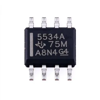
The Texas Instruments TLV2760CD is a single, micropower, rail-to-rail input/output operational amplifier with shutdown, specified for a 1.8 V to 3.6 V supply range, 500 kHz gain-bandwidth product, 20 µA typical quiescent current and an 8-pin SOIC package.

An operational amplifier is a voltage-gain building block that compares two input terminals and drives its output to control loops, buffer levels, or amplify small sensor signals. The TLV2760 belongs to the hierarchy low-noise amplifier -> operational amplifier -> analog signal conditioning IC -> semiconductor, and its rail-to-rail (RRIO) input and output stages let it operate directly across the full supply rails without headroom constraints.

Key features of the TLV2760 include 500 kHz bandwidth from only 20 µA of supply current, rail-to-rail inputs and outputs, a shutdown pin for reducing supply current when the amplifier is idle, 3.5 mV typical offset voltage, and approximately 3 pA input bias current. The wide common-mode input range reaches both supply rails, which simplifies sensor front-ends powered directly from cells.

Architecturally, the device is a CMOS single-supply amplifier that is fully specified down to a 1.8 V rail and characterized at 1.8 V and 2.4 V supply conditions. The maximum recommended supply voltage of 3.6 V permits operation from 1.8 V supplies down to 0.9 V (two AA or AAA cells), giving designers flexibility for energy-harvesting and portable systems.

Typical applications include portable sensor conditioning, battery-powered instrumentation, low-power filter stages, transimpedance pre-amplifiers for photodiodes and pH electrodes, and general embedded signal conditioning where board area and supply current are tightly constrained.

When designing with the TLV2760, keep the shutdown pin compatible with the host logic levels and observe the maximum recommended supply voltage of 3.6 V. Because the amplifier is intended for low-voltage rails, verify that any external feedback network and the surrounding ADC front end operate at compatible common-mode and output swing levels.

This page consolidates distributor availability, drop-in replacement candidates, comparison data and practical layout guidance in one place, so engineers can shortlist the part faster than by reading a datasheet alone.

드롭인 대체품: TLV2760CD — 동일 패키지, 핀 호환. PCB 재작업이 필요한 다른 패키지 부품은 제외됩니다.

이 시리즈의 변형

다음과 드롭인 호환되는 동일 시리즈 모델: TLV2760CD (동일 폼 팩터 및 풋프린트) — 차이점: Amplifier Type, Number of Channels, Operating Temperature Range, Package, RoHS Status.

Texas Instruments
Amplifier Type: CMOS, Rail-to-Rail Input/Output
Number of Channels: 1 (Single)
Operating Temperature Range: -40 °C to +125 °C
비교 대상: TLV2760CD →

TLV2761CD

✅ 드롭인
📦 8-SOIC (0.154 in, 3.90 mm width)
same TLV276x family single amplifier with shutdown in 8-SOIC; identical 1.8 V to 3.6 V supply range and 500 kHz class bandwidth, offset/characterization grade differs

📋 참조 대체품 (카탈로그에 없음)

TLV2760ID

✅ 드롭인
📦 8-SOIC (0.154 in, 3.90 mm width)
same die and 8-SOIC footprint as TLV2760CD but industrial temperature range of -40 °C to 85 °C instead of 0 °C to 70 °C

📋 참조 대체품 (카탈로그에 없음)

TLV2761ID

✅ 드롭인
📦 8-SOIC (0.154 in, 3.90 mm width)
same 8-SOIC single-amplifier family member with shutdown; industrial -40 °C to 85 °C grade versus 0 °C to 70 °C on the TLV2760CD

📋 참조 대체품 (카탈로그에 없음)

TLV9061IDCKR

✅ 드롭인 ⚠️ 사양 미검증
Texas Instruments
📦 8-SOIC (0.154 in, 3.90 mm width)
1 (Single) · CMOS, Rail-to-Rail Input/Output · 10 MHz · 6.5 V/µs · 1.8 V to 5.5 V · 538 µA (typ) · ±0.3 mV · 0.5 pA

가격 문의

데이터시트 보기 →

OPA333UI

✅ 드롭인 ⚠️ 사양 미검증
📦 8-SOIC (0.154 in, 3.90 mm width)
same 8-SOIC single rail-to-rail amplifier footprint, but zero-drift offset of about 50 µV and lower 350 kHz bandwidth versus 3.5 mV and 500 kHz on the TLV2760CD

📋 참조 대체품 (카탈로그에 없음)

MCP6001-I/SN

✅ 드롭인
📦 8-SOIC (0.154 in, 3.90 mm width)
cross-brand 8-SOIC single rail-to-rail CMOS amplifier with about 1 MHz bandwidth and 14 µA typical supply current, but no shutdown pin and a wider 1.8 V to 6 V supply range than the TLV2760CD

📋 참조 대체품 (카탈로그에 없음)

TLV2760CD 최대 정격 & 전기적 특성

Number of Channels 1
Amplifier Type General Purpose Operational Amplifier, Rail-to-Rail Input/Output
Supply Voltage Range 1.8 V to 3.6 V
Maximum Recommended Supply Voltage 3.6 V
Gain-Bandwidth Product 500 kHz
Quiescent Current (Typ) 20 µA per amplifier
Input Offset Voltage (Typ) 3.5 mV
Input Bias Current (Typ) 3 pA
Input Common-Mode Range Rail-to-rail (includes both supply rails)
Output Swing Rail-to-rail
Shutdown Pin Yes
동작 온도 범위 0 °C to 70 °C
패키지 8-SOIC (0.154 in, 3.90 mm width)
실장 유형 Surface Mount
Technology CMOS
RoHS 상태 unknown

TLV2760CD 핀 구성

SOIC-8 Package Pinout Diagram SOIC-8 8-pin small outline IC, 3.9x4.9mm, P1.27mm, JEDEC MS-012. 1 8 2 7 3 6 4 5 SOIC-8
핀 1 OUT — Output voltage
핀 2 V- — Negative supply (ground) connection
핀 3 IN+ — Non-inverting input
핀 4 V- — Negative supply (ground) connection
핀 5 SHDN — Shutdown input; asserted low to enter low-current state
핀 6 IN- — Inverting input
핀 7 V+ — Positive supply connection
핀 8 OUT — Output voltage

일반적인 애플리케이션

TLV2760CD 적합 용도: 6 애플리케이션s: Battery-Powered Sensor Signal Conditioning, Portable Medical and Wearable Monitoring, Transimpedance Photodiode Preamplifier, Low-Power Active Filter Stages, Industrial Process Sensing and Data Acquisition, Low-Voltage Buffering and Level Shifting.

🔋

Battery-Powered Sensor Signal Conditioning

The TLV2760CD suits low-voltage sensor front ends because it operates from a 1.8 V rail, consumes about 20 µA of quiescent current and offers rail-to-rail inputs that accept the full 0 V to 1.8 V output range of a resistive bridge or potentiometer. With 3 pA input bias current, the amplifier does not load the sensor, so a 1 MΩ divider still resolves microvolt-level changes. Place the device directly at the sensor pins and drive the ADC front end from the same 1.8 V cell, keeping the signal path above the ground rail. The shutdown pin lets the node drop to a near-zero current state between readings, which directly extends battery life in handheld meters and environmental monitors.

💊

Portable Medical and Wearable Monitoring

Wearable and portable monitoring devices operate from very small budgets, and the TLV2760CD delivers 500 kHz bandwidth from only 20 µA of supply current. Rail-to-rail input and output stages allow the amplifier to work directly with the small, battery-derived signal swings produced by biopotential or optical sensing front ends without needing a mid-supply bias rail. The 3.5 mV typical input offset translates to a small error term relative to the millivolt-level signals typical in these designs. Use the shutdown input to disable the amplifier while the wearable is in idle or sleep state, and keep the exposed pad-free 8-SOIC footprint easy to route in dense flex-circuit layouts.

📷

Transimpedance Photodiode Preamplifier

The TLV2760CD is a natural choice for transimpedance amplification of photodiode or optical receiver currents because its input bias current of approximately 3 pA produces negligible error across the feedback resistor, and its rail-to-rail input stage accepts the tiny detector voltages at the virtual ground. With 500 kHz gain-bandwidth product, a 10 MΩ feedback resistor still supports useful bandwidth for moderate-speed light measurements. The rail-to-rail output lets the amplified current swing close to the 1.8 V to 3.6 V limits, maximizing usable dynamic range. Keep the feedback network short and guard the input trace against photodiode capacitance to avoid peaking.

🔧

Low-Power Active Filter Stages

Active filter designs in low-voltage embedded systems often need several gain stages but cannot afford the current draw of a general-purpose amplifier family. The TLV2760CD provides 500 kHz gain-bandwidth product at about 20 µA per amplifier, so a multi-stage filter built from this part stays within a tight power envelope. Rail-to-rail inputs and outputs are essential for filter stages referenced to a single 1.8 V rail, since they remove the need for virtual-ground biasing that would otherwise consume headroom. Set component values with the manufacturer datasheet gain-bandwidth and noise figures, and keep the shutdown line asserted when the filtered path is not required.

🏭

Industrial Process Sensing and Data Acquisition

In industrial process monitoring, the TLV2760CD can be used where a low-voltage sensor rail and long battery or loop-powered lifetimes are required. The 3.5 mV typical offset and 3 pA bias current keep the error budget small relative to the 4-20 mA and resistive-divider signals common in process instrumentation, while the 0 °C to 70 °C commercial grade of the TLV2760CD covers standard factory environments. Because the maximum recommended supply is 3.6 V, protection and regulation ahead of the amplifier must keep transients inside that limit. For wider temperature ranges, the TLV2760ID industrial grade offers the same footprint and function.

🖥️

Low-Voltage Buffering and Level Shifting

The TLV2760CD works well as a buffer or level shifter between a low-voltage sensor or logic domain and a downstream ADC or MCU input. Its rail-to-rail input stage accepts signals down to 0 V, and the rail-to-rail output can drive a 1.8 V or 3.3 V domain directly without headroom loss, which non-RR amplifiers cannot do on such tight rails. The approximately 20 µA quiescent current keeps the buffer from dominating the standby budget of an always-on device, and the shutdown input provides a clean way to isolate the buffer during reset or sleep states. Use the manufacturer datasheet output drive capability to confirm the load and capacitive limits for the target node.

What is the operating voltage range of the TLV2760CD?
The TLV2760CD operates from a 1.8 V to 3.6 V single supply, with 3.6 V being the maximum recommended supply voltage. According to the Texas Instruments TLV2760 datasheet, the family is fully specified down to 1.8 V and has been characterized at 1.8 V (the end-of-life condition of two AA cells) and at 2.4 V. That headroom means the part can run directly from a single lithium cell or from a 3 V coin cell, and the low maximum rating protects the amplifier when the rail is a regulated 3.3 V system node.
How much supply current does the TLV2760CD consume?
The TLV2760CD draws about 20 µA of quiescent current per amplifier at typical conditions. The Texas Instruments TLV2760 datasheet describes a family that provides 500 kHz bandwidth from only 20 µA while operating down to 1.8 V over the industrial temperature range. Because the part also includes a shutdown pin, an unused amplifier can be placed in a low-current state during idle periods, which is essential in always-on battery-powered sensor nodes where the amplifier would otherwise dominate the standby budget.
What is the bandwidth and input offset voltage of the TLV2760CD?
The TLV2760CD offers a 500 kHz gain-bandwidth product with a typical input offset voltage of 3.5 mV. The bandwidth figure comes from the Texas Instruments TLV2760 datasheet, and the 3.5 mV offset value is confirmed in distributor parametric listings for this part number. This combination suits signal paths that need modest closed-loop accuracy at microvolt-to-millivolt signal levels, such as current-mode sensor outputs, thermistor bridges and low-side current monitoring.
What is the input bias current of the TLV2760CD?
The TLV2760CD has a typical input bias current of about 3 pA, reflecting its CMOS input stage. Distributor parametric data for this MPN lists the input bias current at 3 pA. Such a low figure makes the amplifier insensitive to source impedance: a 1 MΩ sensor or photodiode bias network will only shift the input by microvolts, so no bias-current compensation resistor is needed in most single-supply front ends.
Does the TLV2760CD support rail-to-rail input and output?
Yes, the TLV2760CD has rail-to-rail inputs and outputs, so the input common-mode range extends to both supply rails and the output swings close to the rails as well. The Texas Instruments TLV2760 datasheet describes the TLV276x single-supply operational amplifiers as rail-to-rail input/output devices. This matters most at low supply voltages: on a 1.8 V rail there is very little headroom, so a non-RR amplifier would clip near mid-supply, whereas the TLV2760 keeps operating over almost the entire 0 V to 1.8 V range.
How does the TLV2760CD compare with the TLV2761CD?
The TLV2760CD and TLV2761CD are sibling devices in the same Texas Instruments TLV276x family of 1.8 V micropower rail-to-rail input/output amplifiers with shutdown, and both are offered in the 8-SOIC package. The two share the same 1.8 V to 3.6 V supply range, 500 kHz class bandwidth and roughly 20 µA supply current. The distinction is device-specific characterization and offset/overhead grading, so consult the family datasheet ordering table to confirm the exact parameters and temperature grades before substituting one for the other.
When should I choose the TLV2760CD instead of the TLV2402ID?
Choose the TLV2760CD when your design runs from a 1.8 V to 3.6 V rail and needs a shutdown function, roughly 20 µA supply current and 500 kHz bandwidth in a single amplifier. Choose the TLV2402ID when you need a dual amplifier in an 8-pin package with higher bandwidth per channel and a wider supply range. The TLV2402ID is a dual, rail-to-rail I/O device with a different pinout arrangement and no shutdown pin in the same functional position, so it is not a pin-for-pin substitute for the TLV2760CD.
Is the TLV2760CD suitable for battery-powered sensor conditioning?
The TLV2760CD is well suited to battery-powered sensor conditioning because it runs from 1.8 V, consumes about 20 µA and offers a shutdown pin for idle periods. Its 3 pA input bias current keeps the error contribution from high-impedance sources negligible, and rail-to-rail inputs let you read a full-range sensor output directly. For example, it can sit directly on a 1.8 V coin-cell node buffering a thermistor or electrochemical sensor before conversion by a low-power ADC.
What is the best drop-in replacement for the TLV2760CD?
The closest pin-compatible replacements are the other members of the Texas Instruments TLV276x family in the 8-SOIC package, specifically the TLV2761CD and the industrial-temperature TLV2760ID and TLV2761ID. Each keeps the same single-amplifier, 8-SOIC pin arrangement with a shutdown pin, so no PCB change is required. If you need more than a like-for-like swap, the TLV9061ID is another 8-SOIC single rail-to-rail part with wider supply range, and cross-brand CMOS single amplifiers in the same footprint can be evaluated in parallel.
What can replace the TLV2760CD in an existing design?
A design built around the TLV2760CD can generally be repopulated with a same-family 8-SOIC device such as the TLV2761CD, which shares the pin arrangement, the 1.8 V to 3.6 V supply range and the shutdown function. The Texas Instruments TLV2760 family datasheet documents these members as drop-in options within the same family. Before swapping, confirm the shutdown pin logic level, the output swing at your rail voltage and the noise/offset figures for the specific grade you choose.
Where can I find the TLV2760CD pinout and datasheet?
The manufacturer pinout is in the Texas Instruments TLV2760 family datasheet, available as a PDF from the TI product page for TLV2760, and the 8-SOIC pin description table gives the exact function of each of the eight pins. Distributor product pages for the TLV2760CD also reproduce the package drawing and pin configuration. Use the pin-description table in the manufacturer datasheet when assigning PCB tracks and when confirming the exposed connections for the shutdown input.
Is the TLV2760CD still active and available for new designs?
The Texas Instruments TLV2760 family is currently an active product line, and the TLV2760CD is offered in the 8-SOIC package across multiple authorized distribution channels. The manufacturer lists the device as active, and distributor parametric pages continue to show standard commercial-temperature ordering options. For current lifecycle status and the latest ordering codes, use the Request a Quote form on this page or the TI product page for the TLV2760.
What is the quiescent current of the TLV2760CD with the shutdown pin asserted?
The TLV2760CD offers a dedicated shutdown input that places the amplifier in a low-current state, but the exact shutdown supply current is not published in the distributor summaries used for this page. The Texas Instruments TLV2760 datasheet is the authoritative document for the shutdown current specification and the shutdown logic levels. In designs where standby current dominates the power budget, pull the shutdown pin to the rail that disables the device and confirm the residual current against the datasheet limit.
How do I get the price and lead time for the TLV2760CD?
Current pricing, stock levels and lead time for the TLV2760CD are handled through the Request a Quote form on this page, which returns the latest commercial terms for the exact package and temperature grade you need. Because the part is a standard single-amplifier 8-SOIC product with an active manufacturer status, it is broadly available. Specify the TLV2760CD ordering code exactly, including the 8-SOIC package and 0 °C to 70 °C commercial temperature range, when requesting the quote.
What are the key specifications of the TLV2760CD that engineers should know?
The TLV2760CD is a single-amplifier 8-SOIC device specified for 1.8 V to 3.6 V supply, 500 kHz gain-bandwidth product, about 20 µA quiescent current, 3.5 mV typical input offset voltage, roughly 3 pA input bias current, rail-to-rail inputs and outputs, and an active shutdown pin over a 0 °C to 70 °C commercial temperature range. According to the Texas Instruments TLV2760 datasheet, the maximum recommended supply voltage of 3.6 V also allows operation from 0.9 V (two AA or AAA cells). These figures make it a micropower general-purpose amplifier for low-voltage portable and sensor applications.
Is the TLV2760CD the same as the MCP6001 for a low-voltage design?
The TLV2760CD and the MCP6001 are both single rail-to-rail CMOS amplifiers offered in an 8-SOIC footprint, so they are frequently compared in low-voltage designs. They differ in detail: the TLV2760CD is characterized for a 1.8 V to 3.6 V supply with a 500 kHz bandwidth, 20 µA quiescent current and an integrated shutdown pin, whereas the MCP6001 targets a wider supply range with roughly 1 MHz bandwidth and a different quiescent-current figure. Verify pin functions, common-mode range and supply limits on each manufacturer's datasheet before interchanging them.

엔지니어링 참조 데이터: TLV2760CD — 비교, 설계 지침 및 규정 준수 정보.

선택 가이드

Choose the TLV2760CD when your design runs from a 1.8 V to 3.6 V rail, needs a rail-to-rail single amplifier with a shutdown pin, and must keep standby current near 20 µA. Choose the TLV2760ID when the same electrical performance is needed over -40 °C to 85 °C, and the TLV2761CD when you prefer the sibling family member with its own offset and characterization grades. Choose the TLV9061ID when you need roughly double the bandwidth or a supply range up to 5.5 V in the same 8-SOIC footprint; it does not reduce the shutdown capability of the family. Choose the OPA333UI when offset drift dominates the error budget and microvolt-level accuracy is required, accepting the higher bandwidth-versus-precision trade-off and the loss of the shutdown pin. Choose the MCP6001-I/SN for a cross-brand single amplifier with about 1 MHz bandwidth and very low supply current, but plan a small firmware and pin-behavior review since it has no shutdown input. In every case, verify the supply limits and common-mode range against your actual rail before finalizing the schematic.

대체품과의 비교

파라미터 이 제품 TLV2761CD TLV2760ID TLV2761ID TLV9061ID OPA333UI MCP6001-I/SN
Package 8-SOIC (0.154 in, 3.90 mm width) 8-SOIC (0.154 in, 3.90 mm width) - same 8-SOIC (0.154 in, 3.90 mm width) - same 8-SOIC (0.154 in, 3.90 mm width) - same 8-SOIC - same 8-SOIC - same 8-SOIC - same
Brand Texas Instruments Texas Instruments Texas Instruments Texas Instruments Texas Instruments Texas Instruments Microchip Technology
Supply Voltage Range 1.8 V to 3.6 V 1.8 V to 3.6 V 1.8 V to 3.6 V 1.8 V to 3.6 V 1.8 V to 5.5 V 1.8 V to 5.5 V 1.8 V to 6.0 V
Gain-Bandwidth Product 500 kHz 500 kHz class 500 kHz 500 kHz class about 1 MHz about 350 kHz about 1 MHz
Quiescent Current (Typ) 20 µA 20 µA class 20 µA 20 µA class about 20 µA about 50 µA about 14 µA
Shutdown Pin Yes Yes Yes Yes Yes No No
Operating Temperature Range 0 °C to 70 °C 0 °C to 70 °C -40 °C to 85 °C -40 °C to 85 °C -40 °C to 125 °C -40 °C to 125 °C -40 °C to 125 °C
Number of Channels 1 1 1 1 1 1 1

주요 차별점

  • Micropower operation with shutdown control (vs MCP6001-I/SN)
  • Lower typical offset than general-purpose CMOS alternatives (vs MCP6001-I/SN)
  • Exact family member for footprint-compatible upgrades (vs TLV2761ID)
  • Higher bandwidth and wider supply range when more headroom is available (vs TLV9061ID)

설계 노트

The TLV2760CD is rated for a maximum recommended supply voltage of 3.6 V. If the amplifier sits behind a regulator that could transiently overshoot, add a clamp or series damping and keep rail noise below 3.6 V under worst-case line conditions. For cell-powered designs, note that the device is specified from 1.8 V and characterized at 1.8 V and 2.4 V, so operating below 1.8 V is outside the guaranteed performance window even though the family tolerates down to 0.9 V supply in some applications.

Because the input bias current is only about 3 pA, the input node is extremely sensitive to leakage from board contamination and to stray capacitance in high-gain transimpedance stages. Keep the inverting input trace short, remove flux residue around the pins, and avoid placing the shutdown pin trace adjacent to the input. Route the shutdown control away from fast-switching nodes so that coupling into the high-impedance input does not appear as output noise.

A frequent design error is assuming a general-purpose rail-to-rail amplifier can be used as a precision reference buffer: the 3.5 mV typical input offset of the TLV2760CD is far larger than a zero-drift part such as the OPA333, so any gain stage near the input of a high-resolution ADC will amplify that offset. Use the shutdown pin only after confirming its logic levels in the manufacturer datasheet, and tie it to a defined state rather than leaving it floating, since a floating high-impedance control pin can pick up noise.

When the TLV2760CD drives a capacitive load such as an ADC sample-and-hold input or a long cable, verify the capacitive load drive specification in the manufacturer datasheet before assuming stability. If the load is highly capacitive, add an isolation resistor between the amplifier output and the load to preserve phase margin. For gain stages above roughly 10, keep the feedback network compact and use low-capacitance, tight-layout components to minimize parasitic poles inside the 500 kHz bandwidth.

규정 준수 정보

RoHS
Unknown
REACH
Unknown
AEC-Q100
Not Applicable
무연
Unknown
무할로겐
Unknown
분쟁 광물
Unknown

The TLV2760 is an industrial/commercial general-purpose amplifier; it is not an AEC-Q100 qualified automotive part. RoHS, REACH, lead-free and halogen-free declarations were not stated in the manufacturer and distributor pages used for this listing, so they are reported as unknown and should be confirmed on the manufacturer product page.

데이터 검증일: 2026-11-04 — XAIPART 부품 엔지니어링 팀이 검증하고 관리한 데이터

관련 검색

TLV2760CD datasheet TLV2760 pinout TLV2760CD 8-SOIC op amp Texas Instruments TLV2760CD TLV2760 500kHz micropower amplifier TLV2760 1.8V rail-to-rail op amp TLV2760CD vs TLV2761CD TLV2760CD vs TLV9061ID TLV2760CD drop-in replacement TLV2760 equivalent single amplifier TLV2760CD price and stock TLV2760 shutdown pin circuit TLV2760 battery powered sensor amplifier TLV2760CD footprint SOIC-8 what is the quiescent current of TLV2760

관련 부품 & 용어

Texas Instruments TLV2760CD TLV2760 TLV2761CD TLV2760ID TLV2761ID TLV9061ID OPA333UI MCP6001-I/SN operational amplifier rail-to-rail input/output amplifier RRIO low-dropout-free CMOS analog IC analog signal conditioning gain-bandwidth product quiescent current input offset voltage input bias current common-mode input range shutdown pin 8-SOIC package SOIC family surface mount SMD battery-powered sensing RoHS REACH
빠른 견적 RFQ
상세 정보를 모두 입력하십시오 — 영업팀이 24시간 이내에 답변드립니다
부품 번호 제조사 패키지 QTY 목표 가격 합계
✓
견적이 제출되었습니다!

24시간 이내에 이메일로 답변드리겠습니다

1
RFQ 제출됨
2
견적 접수됨
3
주문 완료
4
결제
5
배송됨
6
배송 완료
RFQ 상세 보기