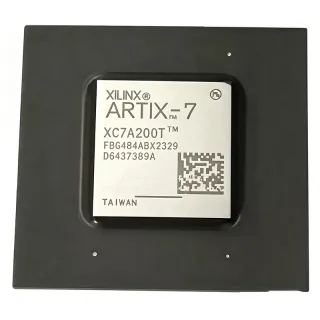
XC6SLX75-3FG484I - 74637-Cell Spartan-6 FPGA | AMD
부품 번호: XC6SLX75-3FG484I ✗ 단종| 수량 | 단가 | 합계 |
|---|---|---|
| 1 | $0 | $0.00 |
| 10 | $0 | $0.00 |
| 100 | $0 | $0.00 |
| 500 | $0 | $0.00 |
| 1,000 | $0 | $0.00 |
XC6SLX75-3FG484I 개요
A field-programmable gate array, or FPGA, is a programmable logic device whose configurable logic blocks, programmable interconnect, block RAM, and digital signal-processing resources can be interconnected after manufacture. Within the semiconductor hierarchy, this device is a Spartan-6 FPGA, then a programmable-logic IC and digital semiconductor. Its large logic capacity and high pin count suit parallel control, protocol bridging, data acquisition, embedded signal processing, and industrial automation systems that need deterministic hardware parallelism.
The verified listings identify 74,637 cells, 45 nm CMOS fabrication, a nominal 1.2 V supply, 280 user I/O, and a 23 mm by 23 mm FBGA-484 package with 1 mm pitch. The -3 grade provides the family’s highest performance positioning according to the supplied specification source. This matters in timing-sensitive designs, but nominal family speed alone does not determine achievable clock frequency; routing, resource type, voltage, temperature, timing constraints, and design effort remain decisive.
The 484-ball package exposes substantially more interconnect than a typical low-pin-count FPGA, making it appropriate for high-bandwidth parallel systems and substantial external memory or peripheral interfaces. Conversely, it requires careful escape routing, via-in-pad-aware assembly, thermal analysis, and BGA-aware inspection. Configuration storage, bank supply requirements, supported I/O standards, and pin constraints must be checked in the official pinout and package files.
Typical uses include industrial machine vision, robotics, test-and-measurement front ends, networking equipment, embedded video control, and high-throughput digital acquisition. The programmable resources allow parallel pipelines and multiple interfaces to coexist without relying entirely on a microcontroller for timing-critical control. For each deployment, engineers should validate memory-mapper resources, clocking, pin assignments, configuration mode, and timing closure in AMD development tools.
A critical design step is to preserve BGA thermal and assembly margin by following AMD package guidelines and validating the completed PCB stack-up. Power rails should be decoupled according to the manufacturer guidance, while clocks and high-speed interfaces require controlled return paths. This page combines verified catalog specifications, sourcing data, and engineering guidance while clearly separating confirmed facts from values requiring further documentation.
드롭인 대체품: XC6SLX75-3FG484I — 동일 패키지, 핀 호환. PCB 재작업이 필요한 다른 패키지 부품은 제외됩니다.
이 시리즈의 변형
다음과 드롭인 호환되는 동일 시리즈 모델: XC6SLX75-3FG484I (동일 폼 팩터 및 풋프린트) — 차이점: Device Type, Mounting Type, Operating Temperature, Package Dimensions, Process Technology.
빠른 비교 도구 — 나란히 비교할 대체 부품을 선택하십시오:
XC6SLX75-3FGG484C
✅ 드롭인📋 참조 대체품 (카탈로그에 없음)
XA6SLX75-3FGG484I
✅ 드롭인📋 참조 대체품 (카탈로그에 없음)
XC6SLX75-N3FG484I
✅ 드롭인📋 참조 대체품 (카탈로그에 없음)
XC6SLX100-3FGG484I
✅ 드롭인📋 참조 대체품 (카탈로그에 없음)
XC6SLX75T-3FGG484I
✅ 드롭인📋 참조 대체품 (카탈로그에 없음)
XC6SLX75-3FG484I 최대 정격 & 전기적 특성
| Device Type | FPGA |
| FPGA Family | Spartan-6 LX |
| Logic Cells | 74,637 cells |
| Configurable Logic Blocks | 5,831 CLBs |
| Process Technology | 45 nm CMOS |
| 공급 전압 | 1.2 V |
| User I/O | 280 I/O |
| Internal Frequency | 667 MHz |
| Catalog Maximum Frequency | 862 MHz |
| Speed Grade | -3 highest-performance family grade |
| Temperature Grade | Industrial |
| 동작 온도 | 0°C to 85°C (32°F to 185°F) |
| 패키지 | FBGA-484 |
| Package Dimensions | 23 mm × 23 mm |
| Package Pitch | 1 mm |
| Terminal Count | 484 balls |
| 실장 유형 | Surface mount |
XC6SLX75-3FG484I 1 mm 핀 구성 가이드
XC6SLX75-3FG484I(1 mm 패키지)의 핀 구성입니다. 이 디지털 IC에는 GPIO, 통신 인터페이스(UART, SPI, I2C), 전원 핀이 포함되어 있습니다. 대체 핀 기능과 구성 옵션은 제조사 데이터시트를 참조하십시오. 임베디드 시스템 설계와 PCB 레이아웃에 필수적입니다.

다음에 대한 상세 핀아웃 데이터 없음: XC6SLX75-3FG484I.
다음을 참조하십시오: 데이터시트 전체 핀 구성은 다음을 참조하십시오.
일반적인 애플리케이션
XC6SLX75-3FG484I 적합 용도: 6 애플리케이션s: Industrial Machine Vision, Robotics and Motion Control, High-Speed Data Acquisition, Networking and Protocol Bridging, Test and Measurement, Embedded Video Processing.
Industrial Machine Vision
The XC6SLX75-3FG484I fits industrial machine-vision controllers that combine image acquisition, thresholding, feature extraction, and actuator control in one programmable device. Its reported 74,637 logic cells and 280 user I/O provide substantial parallelism, while the -3 grade is positioned for performance-sensitive pipelines. A camera interface, sensor-control logic, and real-time decision path can coexist with limited external glue. The 0°C to 85°C listing supports equipment within that enclosure range, but designers must still calculate PCB and junction-temperature margins. Use AMD package files to route the 484-ball BGA, constrain critical interfaces, and validate timing under actual voltage, temperature, and resource conditions.
추천
Robotics and Motion Control
The AMD Spartan-6 LX device is suitable for coordinating encoders, motor-control timing, limit inputs, communications, and safety interlocks in a robotics controller. Its 280 user I/O allows multiple sensor and actuator channels to be connected, while the 74,637-cell fabric can host parallel control blocks instead of relying on a sequential microcontroller for every timing decision. The -3 grade supports the highest-performance family positioning cited in the supplied source. Engineers should separate deterministic timing paths, constrain clock domains, and keep high-current motor switching outside the FPGA. Firmware updates, motor noise, grounding, and fault-response latency also require system-level validation.
추천
High-Speed Data Acquisition
The XC6SLX75-3FG484I can act as the digital back end for a parallel ADC or multi-channel sensor acquisition system. A wide user-I/O complement supports capture buses and control signals, and the programmable fabric can implement buffering, filtering, triggering, packing, and data transfer in parallel. The package pitch of 1 mm and body size of 23 mm by 23 mm require a deliberate high-density PCB layout with short escape routes from the FPGA. Timing closure must use actual ADC and memory interfaces rather than the catalog frequency alone. Engineers should also define test points, control clock skew, isolate analog supplies, and verify bitstream determinism across every acquisition mode.
추천
Networking and Protocol Bridging
The large Spartan-6 LX fabric is useful for protocol conversion, packet processing, test insertion, and low-latency network control where parallel hardware execution is advantageous. Its 280 user I/O can support multiple data paths, while the 74,637 logic cells allow transmit, receive, buffering, and status logic to operate concurrently. The -3 device may be preferable when timing margins are limited, but every high-speed interface must be analyzed with external memory and PHY timing. XAIPART does not supply a verified Ethernet MAC MPN for this specific FPGA in the provided data, so designers should choose the interface companion from the selected reference design and validate pin compatibility, clocking, and protocol-specific licensing requirements.
추천
Test and Measurement
The XC6SLX75-3FG484I is suitable for programmable test logic, sequencing, pattern generation, capture, timing comparison, and instrument-control interfaces. Its 5,831 reported configurable logic blocks and 280 user I/O support parallel channels, while the -3 grade favors timing-critical implementations. The FPGA should be partitioned so acquisition and comparison paths use constrained clocks, while less critical management functions use a separate domain. Calibration data, trigger latency, and instrument safety must remain independent of configuration reloads. Because the verified sources do not provide a specific test-instrument companion circuit, use interface parts validated by the selected instrument architecture and confirm operation across the full 0°C to 85°C listing.
추천
Embedded Video Processing
The Spartan-6 LX FPGA can perform pixel-format conversion, thresholding, timing generation, and interface conditioning in embedded imaging systems that need deterministic parallel pipelines. Its 74,637 logic cells and 280 user I/O provide room for concurrent video timing and control functions, and the -3 grade is identified as the family’s highest-performance option. A practical design should use DDR memory resources for frame buffering and constrain all video timing paths against the selected external memory timing. Power, signal integrity, and heat become more important as logic utilization and memory-interface width increase. Validate LVDS or parallel interfaces through AMD-supported tools and ensure the selected configuration method meets the product’s update-time and recovery requirements.
추천
추천 제품 요약
엔지니어링 참조 데이터: XC6SLX75-3FG484I — 비교, 설계 지침 및 규정 준수 정보.
선택 가이드
대체품과의 비교
| 파라미터 | 이 제품 | XC6SLX75-3FGG484C | XA6SLX75-3FGG484I | XC6SLX75-N3FG484I | XC6SLX100-3FGG484I | XC6SLX75T-3FGG484I |
|---|---|---|---|---|---|---|
| Package | FBGA-484 | FBGA-484 | 484-pin FBGA | 484-BBGA | FBGA-484 | 484-BBGA |
| Brand | AMD | AMD | AMD | AMD | AMD | AMD |
| FPGA Family | Spartan-6 LX | Spartan-6 LX | Spartan-6 family | Spartan-6 LX | Spartan-6 LX | Spartan-6 LXT |
| Logic Cells | 74,637 cells | 74,637 cells | 74,637 cells | 74,637 cells | 100,000 cells | 74,637 cells |
| Speed Grade | -3 | -3 | -3 | -3N | -3 | -3 |
주요 차별점
- XA6SLX75-3FGG484I has the closest supplied equivalence evidence (vs XA6SLX75-3FGG484I)
- Higher logic density is available in the same reported package family (vs XC6SLX100-3FGG484I)
- Target keeps the specified -3 industrial-grade ordering position (vs XC6SLX75-3FGG484C)
- Spartan-6 LXT offers a related -3 package option but changes the device variant (vs XC6SLX75T-3FGG484I)
설계 노트
Design the 484-ball, 1 mm-pitch FBGA with a manufacturer-supported stack-up and escape strategy. The verified package is 23 mm by 23 mm, so placement should preserve routing access to power, ground, configuration, clocks, and high-speed I/O. Check every signal against the official AMD ball map rather than relying on distributor naming variants. Validate drill-to-copper registration, solder-mask definition, via-in-pad usage, and assembly capability before releasing fabrication data.
Implement each required supply rail according to the applicable AMD Spartan-6 design guidance, including local decoupling and sequenced ramp behavior. The supplied data identifies a 1.2 V core supply but does not specify I/O voltages or permitted simultaneous switching limits. Do not infer missing rail values from catalog snippets; obtain them from the manufacturer datasheet and design-support materials. Estimate rail currents and configuration current separately, then include worst-case tolerance, startup, and state-transition margin.
Do not treat either reported frequency as a guaranteed design clock without timing analysis. The supplied sources list both 667 MHz and 862 MHz for catalogs associated with XC6SLX75, illustrating the risk of relying on a single distributor field. Create constraints for every clock domain, analyze post-route timing across the required voltage and 0°C to 85°C operating range, and reserve resources for debug or operational margins. Verify configuration-memory compatibility before programming the first bitstream.
Calculate FPGA and BGA thermal performance from actual utilization, switching activity, supply voltage, ambient temperature, board copper, airflow, and package construction. The provided data does not include a verified theta-JA, theta-JC, or power coefficient, so no numerical junction-temperature claim can be made. Place thermal-critical supply and ground structures according to AMD package guidance, monitor temperature during worst-case workloads, and include derating or shutdown behavior for compact systems with limited airflow.
규정 준수 정보
The supplied search results do not contain explicit material-compliance declarations for the exact ordering code. RoHS, REACH, lead-free, halogen-free, and conflict-minerals status therefore remain unknown. AEC-Q100 is recorded as not applicable because this is an FPGA rather than an automotive-qualified discrete semiconductor.