AD7609BSTZ - 18-Bit 8-Ch Simultaneous Sampling ADC | Analog Devices
MPN: AD7609BSTZ ✓ Active| Qty | Unit Price | Extended |
|---|---|---|
| 1 | $52.63 | $52.63 |
| 10 | $48.5 | $485.00 |
| 100 | $42.1 | $4,210.00 |
| 500 | $36.8 | $18,400.00 |
| 1,000 | $33.2 | $33,200.00 |
AD7609BSTZ Overview
A data acquisition system (DAS) is a complete signal chain that conditions, samples, and converts analog signals into digital data. The AD7609BSTZ belongs to the family of simultaneous sampling ADCs, which capture multiple channels at the same instant to preserve phase relationships between signals. This is critical in applications like three-phase power monitoring and multi-axis motor control, where timing skew between channels would introduce measurement errors. The DAS integrates the entire analog front end, reducing external component count and simplifying design.
Key features include 18-bit resolution with no missing codes, 200 kSPS throughput on all channels, true differential inputs with a ±5 V or ±10 V range, and a 2.5 V internal reference with buffer. The device offers both serial (SPI/DSP) and parallel interfaces, and includes a digital filter for noise reduction. The input clamp protection tolerates voltages up to ±16.5 V, enhancing robustness in industrial environments.
The AD7609BSTZ uses a charge redistribution successive approximation architecture, which provides excellent linearity and low power consumption. The integrated antialiasing filter simplifies external filtering requirements, and the track-and-hold amplifiers ensure accurate sampling of fast-changing signals. The device operates over the industrial temperature range of -40°C to +85°C and is available in a 64-lead LQFP (10x10 mm) package.
Typical applications include power line monitoring, protective relays, motor control, and industrial data acquisition systems. The simultaneous sampling capability is essential for measuring three-phase voltages and currents with accurate phase alignment. The wide input range and robust protection make it suitable for harsh industrial environments.
When designing with the AD7609BSTZ, ensure proper decoupling of the AVCC and DVCC supplies with 10 µF and 0.1 µF capacitors. The REFIN/REFOUT pin can be driven by an external reference for improved accuracy. The digital interface supports both serial and parallel modes, selectable via the PAR/SER/BYTE pin. For best performance, use a low-jitter conversion clock and minimize digital noise coupling to the analog inputs.
Drop-in alternatives for AD7609BSTZ — same package, pin-to-pin compatible. Different-package parts requiring PCB rework are excluded.
Variants in this series
Same-series models that are drop-in compatible with AD7609BSTZ (same form factor and footprint) — differing in Resolution, Input Type, Interface, Internal Reference, Antialiasing Filter.
Quick Comparison Tool — Select alternative parts for side-by-side comparison:
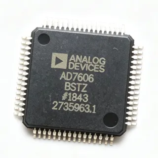
AD7606BSTZ
✅ Drop-In✓ In Stock
$16.9 / Unit
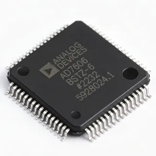
View Datasheet →AD7606BSTZ-RL
✅ Drop-In✓ In Stock
$11.6 / Unit
View Datasheet →AD7609BSTZ-RL
✅ Drop-In📋 Reference alternative (not in catalog)
AD7606C-16BSTZ-RL
✅ Drop-In📋 Reference alternative (not in catalog)
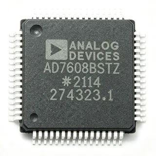
AD7608BSTZ
✅ Drop-In ⚠️ Specs Unverified✓ In Stock
$38.1818 / Unit
View Datasheet →AD7609BSTZ Maximum Ratings & Electrical Characteristics
| Resolution | 18 bits |
| Number of Channels | 8 |
| Input Type | True differential |
| Input Voltage Range | ±5 V or ±10 V |
| Throughput Rate | 200 kSPS |
| Supply Voltage | 5 V (single) |
| Internal Reference | 2.5 V |
| Input Clamp Protection | ±16.5 V |
| Analog Input Impedance | 1 MΩ |
| Interface | SPI, DSP, parallel |
| Package | 64-LQFP (10x10 mm) |
| Operating Temperature Range | -40°C to +85°C |
| Antialiasing Filter | Second-order |
| Architecture | Charge redistribution SAR |
| RoHS | Compliant |
AD7609BSTZ Pin Configuration
| Pin 1 | AVCC — Analog supply voltage (5 V) |
| Pin 2 | V1+ — Positive analog input channel 1 |
| Pin 3 | V1- — Negative analog input channel 1 |
| Pin 4 | V2+ — Positive analog input channel 2 |
| Pin 5 | V2- — Negative analog input channel 2 |
| Pin 6 | V3+ — Positive analog input channel 3 |
| Pin 7 | V3- — Negative analog input channel 3 |
| Pin 8 | V4+ — Positive analog input channel 4 |
| Pin 9 | V4- — Negative analog input channel 4 |
| Pin 10 | V5+ — Positive analog input channel 5 |
| Pin 11 | V5- — Negative analog input channel 5 |
| Pin 12 | V6+ — Positive analog input channel 6 |
| Pin 13 | V6- — Negative analog input channel 6 |
| Pin 14 | V7+ — Positive analog input channel 7 |
| Pin 15 | V7- — Negative analog input channel 7 |
| Pin 16 | V8+ — Positive analog input channel 8 |
| Pin 17 | V8- — Negative analog input channel 8 |
| Pin 18 | AGND — Analog ground |
| Pin 19 | REFIN/REFOUT — Reference input/output |
| Pin 20 | REFCAP — Reference buffer output |
| Pin 21 | REFSELECT — Reference select (high = internal, low = external) |
| Pin 22 | RANGE — Input range select (±5 V or ±10 V) |
| Pin 23 | CONVST A — Conversion start for channels 1-4 |
| Pin 24 | CONVST B — Conversion start for channels 5-8 |
| Pin 25 | BUSY — Busy output (high during conversion) |
| Pin 26 | FRSTDATA — First data output |
| Pin 27 | OS0 — Oversampling ratio bit 0 |
| Pin 28 | OS1 — Oversampling ratio bit 1 |
| Pin 29 | OS2 — Oversampling ratio bit 2 |
| Pin 30 | PAR/SER/BYTE — Parallel/serial/byte select |
| Pin 31 | STBY — Standby mode input |
| Pin 32 | CS — Chip select |
| Pin 33 | RD/SCLK — Read/Serial clock |
| Pin 34 | WR/DIN — Write/Serial data input |
| Pin 35 | DB0 — Parallel data bit 0 |
| Pin 36 | DB1 — Parallel data bit 1 |
| Pin 37 | DB2 — Parallel data bit 2 |
| Pin 38 | DB3 — Parallel data bit 3 |
| Pin 39 | DB4 — Parallel data bit 4 |
| Pin 40 | DB5 — Parallel data bit 5 |
| Pin 41 | DB6 — Parallel data bit 6 |
| Pin 42 | DB7 — Parallel data bit 7 |
| Pin 43 | DB8 — Parallel data bit 8 |
| Pin 44 | DB9 — Parallel data bit 9 |
| Pin 45 | DB10 — Parallel data bit 10 |
| Pin 46 | DB11 — Parallel data bit 11 |
| Pin 47 | DB12 — Parallel data bit 12 |
| Pin 48 | DB13 — Parallel data bit 13 |
| Pin 49 | DB14 — Parallel data bit 14 |
| Pin 50 | DB15 — Parallel data bit 15 |
| Pin 51 | DVCC — Digital supply voltage (5 V) |
| Pin 52 | DGND — Digital ground |
| Pin 53 | VDRIVE — Logic supply voltage |
| Pin 54 | RESET — Reset input |
| Pin 55 | DOUTA — Serial data output A |
| Pin 56 | DOUTB — Serial data output B |
| Pin 57 | DB16 — Parallel data bit 16 |
| Pin 58 | DB17 — Parallel data bit 17 |
| Pin 59 | DB18 — Parallel data bit 18 |
| Pin 60 | DB19 — Parallel data bit 19 |
| Pin 61 | DB20 — Parallel data bit 20 |
| Pin 62 | DB21 — Parallel data bit 21 |
| Pin 63 | DB22 — Parallel data bit 22 |
| Pin 64 | DB23 — Parallel data bit 23 |
Typical Applications
AD7609BSTZ is suitable for 6 applications: Power Line Monitoring, Motor Control, Industrial Data Acquisition, Protective Relays, Three-Phase Power Quality Analysis, Multi-Axis Motion Control.
Power Line Monitoring
The AD7609BSTZ is ideal for power line monitoring due to its 8-channel simultaneous sampling capability and 18-bit resolution. It can measure three-phase voltages and currents with accurate phase alignment, which is critical for protective relays and power quality analysis. The wide input range (±5 V or ±10 V) and robust input protection (±16.5 V) handle the transients common in power systems. The 200 kSPS throughput ensures fast response to grid events, while the integrated antialiasing filter simplifies the analog front end. According to the AD7609 datasheet, the device's high input impedance (1 MΩ) eliminates the need for driver op amps, reducing component count and board space.
Recommended
Motor Control
The AD7609BSTZ is well-suited for motor control applications, particularly field-oriented control (FOC) of AC motors. Its 8-channel simultaneous sampling capability allows precise measurement of multiple phase currents and voltages simultaneously, which is essential for accurate torque and speed control. The 18-bit resolution provides high precision, while the 200 kSPS throughput supports fast control loops. The true differential inputs reject common-mode noise, improving measurement accuracy in noisy industrial environments. According to the AD7609 datasheet, the device's integrated antialiasing filter and high input impedance simplify the analog front end, reducing design complexity and cost.
Recommended
Industrial Data Acquisition
The AD7609BSTZ is a complete data acquisition system (DAS) that integrates the entire analog front end, making it ideal for industrial data acquisition applications. It features 8 true differential input channels with ±5 V or ±10 V ranges, 18-bit resolution, and 200 kSPS throughput. The device includes input clamp protection up to ±16.5 V, a second-order antialiasing filter, and a 2.5 V internal reference. According to the AD7609 datasheet, the high input impedance (1 MΩ) eliminates the need for external driver op amps, simplifying design. The serial and parallel interfaces provide flexibility for connecting to various microcontrollers and DSPs.
Recommended
Protective Relays
The AD7609BSTZ is designed for protective relays in power systems, where accurate and simultaneous measurement of voltage and current is critical. Its 8-channel simultaneous sampling capability ensures phase alignment between channels, which is essential for calculating power and detecting faults. The 18-bit resolution provides high accuracy, while the 200 kSPS throughput enables fast response to transient events. The device's input clamp protection (±16.5 V) and wide input range (±5 V or ±10 V) handle the harsh conditions of power systems. According to the AD7609 datasheet, the integrated antialiasing filter and high input impedance simplify the analog front end, reducing component count and improving reliability.
Recommended
Three-Phase Power Quality Analysis
The AD7609BSTZ is ideal for three-phase power quality analysis, where simultaneous sampling of multiple voltage and current channels is required to accurately compute power parameters such as active power, reactive power, and harmonics. The device's 8 channels can measure three-phase voltages and currents simultaneously, preserving phase relationships. The 18-bit resolution and 200 kSPS throughput provide the accuracy and speed needed for detailed harmonic analysis. According to the AD7609 datasheet, the true differential inputs reject common-mode noise, improving measurement accuracy in industrial environments. The integrated antialiasing filter simplifies external filtering, reducing design complexity.
Recommended
Multi-Axis Motion Control
The AD7609BSTZ is suitable for multi-axis motion control systems, where simultaneous sampling of position and current feedback signals is essential for coordinated motion. Its 8-channel simultaneous sampling capability allows precise measurement of multiple axes at the same instant, ensuring accurate synchronization. The 18-bit resolution provides high precision, while the 200 kSPS throughput supports fast control loops. The true differential inputs reject common-mode noise, improving measurement accuracy in noisy industrial environments. According to the AD7609 datasheet, the device's integrated antialiasing filter and high input impedance simplify the analog front end, reducing design complexity and cost.
Recommended
Recommended Products Summary
Engineering reference data for AD7609BSTZ — comparison, design guidance, and compliance information.
Selection Guide
Comparison with Alternatives
| Parameter | This Product | AD7606BSTZ | AD7606BSTZ-RL | AD7609BSTZ-RL | AD7606C-16BSTZ-RL | AD7608BSTZ |
|---|---|---|---|---|---|---|
| Package | 64-LQFP (10x10 mm) | 64-LQFP (10x10 mm) | 64-LQFP (10x10 mm) | 64-LQFP (10x10 mm) | 64-LQFP (10x10 mm) | 64-LQFP (10x10 mm) |
| Brand | Analog Devices | Analog Devices | Analog Devices | Analog Devices | Analog Devices | Analog Devices |
| Resolution | 18 bits | 16 bits | 16 bits | 18 bits | 16 bits | 14 bits |
| Number of Channels | 8 | 8 | 8 | 8 | 8 | 8 |
| Throughput Rate | 200 kSPS | 200 kSPS | 200 kSPS | 200 kSPS | 200 kSPS | 200 kSPS |
| Input Voltage Range | ±5 V or ±10 V | ±5 V or ±10 V | ±5 V or ±10 V | ±5 V or ±10 V | ±5 V or ±10 V | ±5 V or ±10 V |
| Interface | SPI, DSP, parallel | SPI, DSP, parallel | SPI, DSP, parallel | SPI, DSP, parallel | SPI, DSP, parallel | SPI, DSP, parallel |
| Supply Voltage | 5 V | 5 V | 5 V | 5 V | 5 V | 5 V |
Key Differentiators
- 18-bit resolution with 8 simultaneous sampling channels (vs AD7606BSTZ)
- True differential inputs with ±16.5 V clamp protection (vs AD7608BSTZ)
- 200 kSPS throughput on all channels simultaneously (vs AD7606C-16BSTZ-RL)
Design Notes
Decouple the AVCC and DVCC supplies with 10 µF and 0.1 µF capacitors placed close to the pins. Use a low-impedance ground plane to minimize noise coupling. The AD7609BSTZ operates from a single 5 V supply, simplifying power design. According to the AD7609 datasheet, proper decoupling is essential for achieving the specified 18-bit performance.
Place the AD7609BSTZ on a PCB with a solid ground plane and separate analog and digital ground areas. Keep analog input traces short and shielded to minimize noise pickup. The device's high input impedance (1 MΩ) reduces the need for driver op amps, but proper layout is still critical for maintaining signal integrity. According to the AD7609 datasheet, the input clamp protection tolerates voltages up to ±16.5 V, providing robustness in industrial environments.
Ensure the REF SELECT pin is set correctly: high for internal reference, low for external. If using an external reference, apply it to the REFIN pin. The RANGE pin selects ±5 V or ±10 V input range; set it according to your signal levels. According to the AD7609 datasheet, the PAR/SER/BYTE pin selects the interface mode; ensure it is configured correctly for your microcontroller. Avoid exceeding the absolute maximum ratings on any pin.
Compliance Information
RoHS compliance confirmed by distributor listings. Other compliance data not explicitly stated in the provided data.