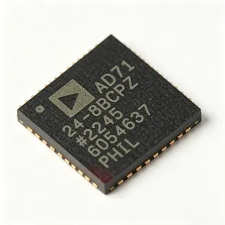
ADADC85S12/883B - 12-Bit SAR ADC, 10us | Analog Devices
MPN: ADADC85S12/883B ✓ Active| Qty | Unit Price | Extended |
|---|---|---|
| 1 | $150 | $150.00 |
| 10 | $135 | $1,350.00 |
| 100 | $120 | $12,000.00 |
| 500 | $105 | $52,500.00 |
| 1,000 | $90 | $90,000.00 |
ADADC85S12/883B Overview
An analog-to-digital converter (ADC) is a critical component in electronic systems that converts continuous analog signals into discrete digital values for processing by digital circuits. The ADADC85S12/883B is a successive approximation register (SAR) ADC, which uses a binary search algorithm to determine the digital output. SAR ADCs are known for their high speed and moderate resolution, making them suitable for applications such as data acquisition, industrial control, and military instrumentation. The ADADC85S12/883B integrates the clock, reference, and comparator on-chip, reducing external component count and simplifying design.
Key features of the ADADC85S12/883B include 12-bit resolution, a 10-microsecond conversion time, and an internal reference and clock. The device operates from a single +5V supply and provides parallel output data. The MIL-STD-883 Class B screening ensures high reliability for defense and aerospace applications. The SBDIP package offers excellent thermal performance and is suitable for through-hole mounting.
The ADADC85S12/883B uses a hybrid IC design that combines MSI digital and linear monolithic chips with a 12-bit monolithic DAC. This architecture provides modular performance and versatility while maintaining a compact size and low cost. The internal comparator and reference are trimmed for accuracy, ensuring consistent performance across the operating temperature range.
Typical applications include military avionics, radar systems, missile guidance, and high-reliability industrial data acquisition. The device's wide temperature range and MIL-STD-883 qualification make it ideal for harsh environments. When designing with this ADC, ensure proper decoupling on the power supply and reference pins to minimize noise and achieve specified performance.
Drop-in alternatives for ADADC85S12/883B — same package, pin-to-pin compatible. Different-package parts requiring PCB rework are excluded.
Variants in this series
Same-series models that are drop-in compatible with ADADC85S12/883B (same form factor and footprint) — differing in Architecture, Mounting Type, Package.
Quick Comparison Tool — Select alternative parts for side-by-side comparison:
ADADC85S-12/883B
✅ Drop-In✓ In Stock
$175 / Unit
View Datasheet →ADADC85S-12
✅ Drop-In📋 Reference alternative (not in catalog)
ADADC85S-10/883B
✅ Drop-In ⚠️ Specs Unverified📋 Reference alternative (not in catalog)
ADADC85S-12/883B
✅ Drop-In✓ In Stock
$175 / Unit
View Datasheet →ADADC85S-12
✅ Drop-In📋 Reference alternative (not in catalog)
ADADC85S-10/883B
✅ Drop-In ⚠️ Specs Unverified📋 Reference alternative (not in catalog)
ADADC85S12/883B Maximum Ratings & Electrical Characteristics
| Resolution | 12 bits |
| Conversion Time | 10 us |
| Architecture | SAR |
| Number of Inputs | 1 |
| Input Type | Single-Ended |
| Data Interface | Parallel |
| Reference Type | Internal |
| Supply Voltage | 5 V |
| Operating Temperature Range | -55°C to +125°C |
| Package | 32-SBDIP-H |
| Mounting Type | Through Hole |
| Screening Level | MIL-STD-883 Class B |
| RoHS Status | unknown |
| REACH Status | unknown |
| AEC-Q100 | not_applicable |
ADADC85S12/883B Pin Configuration
| Pin 1 | VCC — Positive supply voltage (5V) |
| Pin 2 | GND — Ground |
| Pin 3 | VREF — Reference voltage output |
| Pin 4 | AIN — Analog input |
| Pin 5 | CLK — Clock input (internal clock used) |
| Pin 6 | CONVST — Conversion start input |
| Pin 7 | BUSY — Busy output indicating conversion in progress |
| Pin 8 | DB0 — Data bit 0 (LSB) |
| Pin 9 | DB1 — Data bit 1 |
| Pin 10 | DB2 — Data bit 2 |
| Pin 11 | DB3 — Data bit 3 |
| Pin 12 | DB4 — Data bit 4 |
| Pin 13 | DB5 — Data bit 5 |
| Pin 14 | DB6 — Data bit 6 |
| Pin 15 | DB7 — Data bit 7 |
| Pin 16 | DB8 — Data bit 8 |
| Pin 17 | DB9 — Data bit 9 |
| Pin 18 | DB10 — Data bit 10 |
| Pin 19 | DB11 — Data bit 11 (MSB) |
| Pin 20 | CS — Chip select input |
| Pin 21 | RD — Read input |
| Pin 22 | WR — Write input |
| Pin 23 | GND — Ground |
| Pin 24 | VCC — Positive supply voltage (5V) |
Typical Applications
ADADC85S12/883B is suitable for 6 applications: Military Avionics, Radar Systems, Missile Guidance, Industrial Data Acquisition, Test and Measurement, Aerospace Telemetry.
Military Avionics
The ADADC85S12/883B is ideal for military avionics due to its MIL-STD-883 Class B screening and wide temperature range. It converts analog sensor signals from flight control systems into digital data for processing. Its 12-bit resolution ensures accurate measurement of altitude, speed, and attitude, while the 10us conversion time supports real-time control loops. The internal reference and clock reduce external components, saving space in space-constrained avionics modules.
Recommended
Radar Systems
In radar systems, the ADADC85S12/883B digitizes the received IF signal for target detection and ranging. Its 10us conversion time allows sampling of fast-rising pulses, while the 12-bit resolution provides the dynamic range needed to distinguish small targets from clutter. The device's military temperature rating ensures reliable operation in the harsh thermal environment of radar transceivers. The parallel interface simplifies connection to DSPs for real-time signal processing.
Recommended
Missile Guidance
The ADADC85S12/883B is used in missile guidance systems to convert analog signals from inertial sensors and seeker electronics into digital form for navigation algorithms. Its MIL-STD-883 qualification ensures high reliability in extreme vibration and temperature conditions. The 12-bit resolution provides precise measurement of acceleration and angular rate, while the 10us conversion time supports high-bandwidth control loops. The internal reference and clock reduce board space, critical for compact missile electronics.
Recommended
Industrial Data Acquisition
The ADADC85S12/883B is well-suited for industrial data acquisition systems that require high reliability and wide temperature operation. It converts analog signals from sensors such as temperature, pressure, and flow into digital data for monitoring and control. Its 12-bit resolution provides adequate accuracy for most industrial measurements, while the 10us conversion time allows sampling of fast-changing signals. The parallel interface enables easy integration with microcontrollers and PLCs.
Recommended
Test and Measurement
In test and measurement equipment, the ADADC85S12/883B provides accurate digitization of analog signals for analysis. Its 12-bit resolution and 10us conversion time make it suitable for oscilloscopes, spectrum analyzers, and data loggers. The device's wide temperature range ensures stable performance in benchtop and field environments. The parallel interface allows high-speed data transfer to the host processor, enabling real-time waveform display and analysis.
Recommended
Aerospace Telemetry
The ADADC85S12/883B is used in aerospace telemetry systems to convert analog sensor data into digital format for transmission to ground stations. Its MIL-STD-883 qualification ensures reliable operation in the space environment, including radiation and extreme temperatures. The 12-bit resolution provides accurate measurement of parameters such as engine performance and structural stress. The 10us conversion time supports high-speed data streaming, while the internal reference and clock reduce component count in space-constrained telemetry units.
Recommended
Recommended Products Summary
Engineering reference data for ADADC85S12/883B — comparison, design guidance, and compliance information.
Selection Guide
Comparison with Alternatives
| Parameter | This Product | ADADC85S-12/883B | ADADC85S-12 | ADADC85S-10/883B |
|---|---|---|---|---|
| Resolution | 12 bits | 12 bits | 12 bits | 10 bits |
| Conversion Time | 10 us | 10 us | 10 us | 10 us |
| Package | 32-SBDIP-H | 32-SBDIP-H | 32-SBDIP-H | 32-SBDIP-H |
| Brand | Analog Devices | Analog Devices | Analog Devices | Analog Devices |
| MIL-STD-883 | Class B | Class B | No | Class B |
| Operating Temperature | -55°C to +125°C | -55°C to +125°C | -55°C to +125°C | -55°C to +125°C |
| Supply Voltage | 5V | 5V | 5V | 5V |
| Data Interface | Parallel | Parallel | Parallel | Parallel |
Key Differentiators
- MIL-STD-883 Class B screening (vs ADADC85S-12)
- 12-bit resolution (vs ADADC85S-10/883B)
- Internal reference and clock (vs External reference ADCs)
Design Notes
The ADADC85S12/883B requires a clean +5V supply. Use a low-dropout regulator with low output noise and adequate decoupling. Place 0.1uF and 10uF capacitors close to the VCC pins to filter high-frequency noise and provide transient current. Ensure the ground plane is solid and connected to the GND pins with minimal impedance.
For optimal performance, keep the analog input trace short and shielded from digital signals. Use a ground plane under the ADC to minimize noise coupling. Separate analog and digital ground planes and connect them at a single point near the ADC. Place the reference bypass capacitor close to the VREF pin to ensure stable reference voltage.
Do not exceed the absolute maximum ratings for supply voltage and input voltage. Ensure the analog input is within the specified input range to avoid damage. The internal reference is trimmed, but external loading can affect accuracy; buffer the reference output if driving external loads. Also, ensure proper timing for the conversion start signal to avoid metastability.
Compliance Information
Compliance information not provided in the verified data. This is a military-grade component, so RoHS/REACH compliance may not be applicable or may differ from commercial parts.