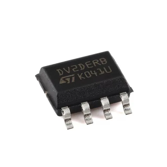
ST25DV04K-IER6S3 - 4Kbit Dynamic NFC/RFID Tag IC | STMicroelectronics
MPN: ST25DV04K-IER6S3 ✓ Active| Qty | Unit Price | Extended |
|---|---|---|
| 1 | $0.9545 | $0.95 |
| 10 | $0.6894 | $6.89 |
| 100 | $0.6098 | $60.98 |
| 500 | $0.5833 | $291.65 |
| 1,000 | $0.5568 | $556.80 |
ST25DV04K-IER6S3 Overview
What is a dynamic NFC/RFID tag IC? A dynamic NFC/RFID tag IC is a type of RFID transponder that combines a contactless RF interface with a wired interface (typically I2C) to allow a microcontroller to read and write the tag's memory both over the air and via the wired bus. This category sits within the broader hierarchy: NFC/RFID tag IC -> RFID transponder -> RFID/NFC integrated circuit -> wireless communication IC -> semiconductor. The dynamic nature means the tag can be updated in real time by the host MCU, enabling use cases like wireless configuration, data logging, and product authentication.
Key features include 4 Kbit EEPROM organized in 128-byte pages, an I2C interface with a 1 MHz clock, an RF interface compliant with ISO 15693 and ISO 18000-3 Mode 1, a 64-bit unique identifier (UID), and an energy harvesting function that can power external circuits. The device supports a wide supply voltage range of 1.8V to 5.5V on the I2C side, and it includes an interrupt output to signal RF activity. The SO-8 package is compact and suitable for surface-mount assembly.
Technically, the ST25DV04K-IER6S3 integrates an RF front-end with an analog-to-digital converter for energy harvesting, a state machine for protocol handling, and a memory controller for EEPROM access. The EEPROM is organized into 32 pages of 128 bits each, with a data retention of 10 years and an endurance of 1 million write cycles. The device supports both static and dynamic memory mapping, allowing the host to control which memory areas are accessible over RF.
Typical applications include smart home devices (e.g., smart locks, thermostats), industrial equipment configuration, consumer electronics pairing (e.g., Bluetooth speakers, wearables), and medical device calibration. The energy harvesting feature enables battery-less operation for low-power sensors, and the I2C interface allows seamless integration with microcontrollers.
When designing with this device, ensure proper antenna matching for the RF interface and place decoupling capacitors close to the VCC pin. The energy harvesting output should be buffered with a capacitor to provide stable power to external circuits. Also, consider the I2C address configuration via the RF field to avoid conflicts in multi-tag systems.
This page synthesizes distributor pricing, drop-in alternatives, and practical design notes not found in the STMicroelectronics datasheet, providing a comprehensive resource for engineers evaluating the ST25DV04K-IER6S3.
Drop-in alternatives for ST25DV04K-IER6S3 — same package, pin-to-pin compatible. Different-package parts requiring PCB rework are excluded.
Variants in this series
Same-series models that are drop-in compatible with ST25DV04K-IER6S3 (same form factor and footprint) — differing in Energy Harvesting, Package.
Quick Comparison Tool — Select alternative parts for side-by-side comparison:
ST25DV04K-IER6S1
📋 Reference alternative (not in catalog)
ST25DV04K-IER6S2
📋 Reference alternative (not in catalog)
ST25DV04K-IER6S4
📋 Reference alternative (not in catalog)
ST25DV04K-IER6S3 Specifications (manufacturer-published)
| Memory Size | 4 Kbit (512 bytes) EEPROM |
| RF Interface | ISO 15693 / ISO 18000-3 Mode 1 |
| Operating Frequency | 13.56 MHz |
| RF Data Rate | 53 kbit/s (downlink), 26 kbit/s (uplink) |
| I2C Interface | Up to 1 MHz |
| Supply Voltage (I2C) | 1.8 V to 5.5 V |
| Energy Harvesting | Yes, up to 5 mA output |
| Unique Identifier (UID) | 64-bit |
| Data Retention | 10 years |
| Write Endurance | 1 million cycles |
| Operating Temperature | -40°C to +85°C |
| Package | SO-8 (NXP-style) |
| Mounting Type | Surface Mount |
| RoHS Status | Compliant |
| REACH Status | Compliant |
ST25DV04K-IER6S3 Pin Configuration
| Pin 1 | VCC — Power supply (1.8V to 5.5V) |
| Pin 2 | GND — Ground |
| Pin 3 | SCL — I2C clock line |
| Pin 4 | SDA — I2C data line |
| Pin 5 | RF1 — RF antenna connection 1 |
| Pin 6 | RF2 — RF antenna connection 2 |
| Pin 7 | INT — Interrupt output (active low) |
| Pin 8 | EH — Energy harvesting output |
Power & Thermal Characteristics
| Power Input | 1.8 V to 5.5 V |
| Operating Temperature | -40°C to +85°C |
Power input and thermal parameters for ST25DV04K-IER6S3 as published by the manufacturer.
Typical Applications
ST25DV04K-IER6S3 is suitable for 6 applications: Smart Home Device Configuration, Industrial Equipment Configuration, Consumer Electronics Pairing, Medical Device Calibration, Battery-less Sensor Node, Product Authentication.
Smart Home Device Configuration
The ST25DV04K-IER6S3 enables wireless configuration of smart home devices such as smart locks, thermostats, and lighting controls. Its dynamic NFC capability allows a smartphone to write configuration parameters (e.g., Wi-Fi credentials, user settings) to the tag over the air, while the I2C interface lets the host MCU read and apply these settings. The 4 Kbit memory is sufficient for storing multiple configuration profiles, and the energy harvesting feature can power a small LED indicator during NFC communication. The device's ISO 15693 compliance ensures compatibility with standard NFC-enabled smartphones and readers, providing a seamless user experience. In a typical smart lock application, the ST25DV04K is placed near the lock's antenna, and the MCU reads the tag via I2C to authenticate users or update access codes. The wide supply voltage range (1.8V to 5.5V) allows direct connection to common MCU power rails, simplifying the design. The interrupt output can signal the MCU when an RF write occurs, enabling real-time updates. Overall, the ST25DV04K-IER6S3 provides a cost-effective and reliable solution for smart home device configuration, reducing the need for physical buttons or complex pairing procedures.
Recommended
Industrial Equipment Configuration
In industrial settings, the ST25DV04K-IER6S3 is used for equipment configuration and maintenance. It allows technicians to wirelessly read and write machine parameters, firmware versions, and calibration data using a handheld NFC reader. The 4 Kbit memory can store a machine's serial number, maintenance logs, and configuration settings. The I2C interface enables the equipment's main controller to access this data for diagnostics and automated setup. The device's wide operating temperature range (-40°C to +85°C) makes it suitable for harsh industrial environments. The energy harvesting feature can power a small status LED or sensor, eliminating the need for a battery. In a typical application, the ST25DV04K is mounted on a PCB inside the equipment, with an antenna connected to the RF pins. When a technician taps the equipment with an NFC-enabled device, the tag provides real-time data, and the technician can update parameters without opening the enclosure. This reduces downtime and improves maintenance efficiency. The ISO 15693 compliance ensures interoperability with standard industrial RFID readers, and the 1 MHz I2C interface allows fast data transfer to the host controller. Overall, the ST25DV04K-IER6S3 enhances industrial equipment usability and maintainability.
Recommended
Consumer Electronics Pairing
The ST25DV04K-IER6S3 simplifies pairing of consumer electronics such as Bluetooth speakers, wearables, and smart accessories. By embedding the tag in the device, users can tap their NFC-enabled smartphone to automatically initiate Bluetooth pairing, transfer Wi-Fi credentials, or launch a companion app. The 4 Kbit memory can store pairing keys, device information, and user preferences. The I2C interface allows the device's main MCU to update the tag data dynamically, such as changing the device name or updating firmware status. The energy harvesting feature can power a small LED to indicate successful pairing. In a typical Bluetooth speaker, the ST25DV04K is connected to the speaker's MCU via I2C, and the antenna is integrated into the speaker's enclosure. When a user taps the speaker with a smartphone, the tag provides the necessary pairing information, and the smartphone automatically connects. This eliminates the need for manual Bluetooth discovery and PIN entry, enhancing user experience. The device's small SO-8 package is ideal for space-constrained consumer products, and its low power consumption ensures minimal impact on battery life. Overall, the ST25DV04K-IER6S3 enables seamless and intuitive pairing for a wide range of consumer electronics.
Recommended
Medical Device Calibration
The ST25DV04K-IER6S3 is used in medical devices for calibration and data logging. It allows manufacturers to store calibration coefficients, manufacturing date, and device serial numbers in the tag, which can be read wirelessly during quality control or maintenance. The 4 Kbit memory is sufficient for storing calibration data for multiple parameters. The I2C interface enables the device's microcontroller to read and update the calibration data during operation. The energy harvesting feature can power a small sensor or indicator, reducing the need for batteries. In a typical medical device, such as a blood glucose meter, the ST25DV04K is placed on the PCB, and the antenna is integrated into the device's housing. During manufacturing, calibration data is written to the tag via I2C. During use, a technician can read the data with an NFC reader to verify calibration or update it if needed. The device's wide operating temperature range and high write endurance (1 million cycles) ensure reliable performance over the device's lifetime. The ISO 15693 compliance ensures compatibility with standard medical-grade NFC readers. Overall, the ST25DV04K-IER6S3 provides a secure and convenient method for managing calibration data in medical devices, improving accuracy and traceability.
Recommended
Battery-less Sensor Node
The ST25DV04K-IER6S3 can be used in battery-less sensor nodes, where the energy harvesting feature powers the sensor and the tag provides data storage and communication. The tag can harvest energy from the RF field of an NFC reader, providing up to 5 mA to power external circuits. This enables the sensor to take measurements and store them in the tag's memory, which can be read wirelessly when the reader is present. The 4 Kbit memory can store sensor readings, timestamps, and configuration data. The I2C interface allows the sensor's MCU to write data to the tag, and the RF interface allows the reader to retrieve it. In a typical application, a temperature sensor is connected to the ST25DV04K's energy harvesting output, and the sensor's MCU reads the temperature and writes it to the tag via I2C. When a reader is brought near, the tag transmits the data over RF. This eliminates the need for batteries, reducing maintenance and environmental impact. The device's low power consumption and wide operating temperature range make it suitable for remote or harsh environments. Overall, the ST25DV04K-IER6S3 enables the development of self-powered, wireless sensor nodes for IoT applications.
Recommended
Product Authentication
The ST25DV04K-IER6S3 can be used for product authentication and anti-counterfeiting. By storing a unique identifier and authentication data in the tag, manufacturers can verify the authenticity of their products. The 64-bit UID is unique to each tag, and additional authentication data can be stored in the 4 Kbit memory. The I2C interface allows the product's MCU to read the authentication data and verify it locally, while the RF interface allows consumers or inspectors to verify authenticity with an NFC-enabled smartphone. In a typical application, a luxury goods manufacturer embeds the ST25DV04K in the product packaging. The tag stores a cryptographic hash or digital signature that can be verified using a public key. When a consumer taps the packaging with a smartphone, the phone reads the tag and verifies the signature, confirming the product's authenticity. The energy harvesting feature can power a small LED to indicate successful verification. The device's high write endurance and data retention ensure long-term reliability. Overall, the ST25DV04K-IER6S3 provides a robust and user-friendly solution for product authentication, helping to protect brand reputation and revenue.
Recommended
Recommended Products Summary
Engineering reference data for ST25DV04K-IER6S3 — comparison, design guidance, and compliance information.
Selection Guide
Comparison with Alternatives
| Parameter | This Product | ST25DV04K-IER6S1 | ST25DV04K-IER6S2 | ST25DV04K-IER6S4 |
|---|---|---|---|---|
| Package | SO-8 | SO-8 | SO-8 | SO-8 |
| Memory Size | 4 Kbit | 4 Kbit | 4 Kbit | 4 Kbit |
| RF Interface | ISO 15693 / ISO 18000-3 Mode 1 | ISO 15693 / ISO 18000-3 Mode 1 | ISO 15693 / ISO 18000-3 Mode 1 | ISO 15693 / ISO 18000-3 Mode 1 |
| I2C Clock Frequency | 1 MHz | 1 MHz | 1 MHz | 1 MHz |
| Supply Voltage | 1.8V to 5.5V | 1.8V to 5.5V | 1.8V to 5.5V | 1.8V to 5.5V |
| Energy Harvesting | Yes (up to 5 mA) | Yes (up to 5 mA) | Yes (up to 5 mA) | Yes (up to 5 mA) |
| Operating Temperature | -40°C to +85°C | -40°C to +85°C | -40°C to +85°C | -40°C to +85°C |
| Unique Identifier | 64-bit | 64-bit | 64-bit | 64-bit |
Key Differentiators
- Energy harvesting capability (vs ST25DV04K-IER6S1)
- Wide supply voltage range (vs ST25DV04K-IER6S2)
- ISO 15693 compliance (vs ST25DV04K-IER6S4)
Design Notes
For optimal RF performance, the antenna should be tuned to 13.56 MHz and matched to the RF1 and RF2 pins. Use a PCB antenna or a ferrite antenna with appropriate matching components (e.g., a capacitor in parallel). Keep the antenna away from ground planes and metal objects to avoid detuning. Place the tag IC close to the antenna to minimize trace length.
The VCC pin should be decoupled with a 100 nF capacitor placed as close as possible to the pin. If using the energy harvesting output (EH), add a storage capacitor (e.g., 10 uF) to smooth the harvested energy and provide stable power to external circuits. Ensure the total current draw from EH does not exceed 5 mA.
Do not apply voltage to the RF pins (RF1, RF2) as they are directly connected to the antenna and are not designed for DC bias. Also, ensure the I2C address is configured correctly to avoid conflicts with other devices on the bus. The default address is 0x53, but it can be changed via RF commands.
Compliance Information
RoHS and REACH compliant per STMicroelectronics product page. Not AEC-Q100 qualified as it is not an automotive-grade component.






