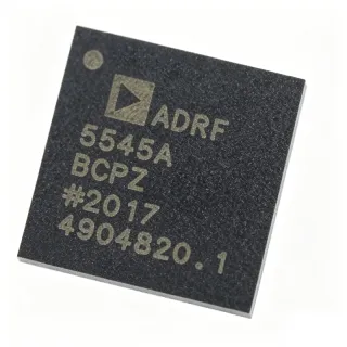
ADRF5547BCPZN - Dual-Channel RF Front End 3.7-5.3GHz | Analog Devices
MPN: ADRF5547BCPZN ✓ Active| Qty | Unit Price | Extended |
|---|---|---|
| 1 | $17.65 | $17.65 |
| 10 | $16.5 | $165.00 |
| 100 | $15.2 | $1,520.00 |
| 500 | $14.1 | $7,050.00 |
| 1,000 | $13 | $13,000.00 |
ADRF5547BCPZN Overview
An RF front end (RFFE) is the circuitry between the antenna and the digital baseband in a wireless transceiver. It typically includes low noise amplifiers (LNAs), power amplifiers (PAs), switches, filters, and matching networks. The ADRF5547 integrates the LNA and SPDT switch into a single module, reducing component count and improving performance by minimizing interconnect losses. This module is part of the broader RF front-end category, which is essential for signal conditioning in both transmit and receive paths.
Key features include a noise figure of 1.6 dB, which ensures high receiver sensitivity, and a 40W SPDT switch capable of handling high transmit power. The dual-channel configuration supports diversity or MIMO applications, and the module operates over a wide supply voltage range. The LFCSP-VQ package offers excellent thermal performance and a small footprint, ideal for dense PCB layouts.
Technically, the ADRF5547 uses a silicon SPDT switch with high linearity and power handling, while the two-stage LNA provides high gain and low noise. The module is designed for TDD systems where the same antenna is used for both transmit and receive, requiring fast switching between modes. The integrated design ensures minimal insertion loss and high isolation between channels.
Typical applications include 5G NR base stations, small cells, massive MIMO arrays, and other TDD wireless infrastructure. The wide frequency range covers n77, n78, and n79 bands, making it versatile for global deployments. The module's high linearity and low noise make it suitable for both sub-6 GHz macro and small cell applications.
When designing with the ADRF5547, ensure proper grounding and thermal management for the LFCSP-VQ package. The exposed pad should be soldered to a thermal via array to dissipate heat from the high-power switch. Also, consider the control logic timing for TDD switching to avoid signal degradation during transitions.
Drop-in alternatives for ADRF5547BCPZN — same package, pin-to-pin compatible. Different-package parts requiring PCB rework are excluded.
Variants in this series
Same-series models that are drop-in compatible with ADRF5547BCPZN (same form factor and footprint) — differing in Frequency Range.
Quick Comparison Tool — Select alternative parts for side-by-side comparison:
ADRF5545ABCPZN
✅ Drop-In✓ In Stock
$16.19 / Unit
View Datasheet →ADRF5547BCPZN-R7
✅ Drop-In📋 Reference alternative (not in catalog)
ADRF5547BCPZN-RL
✅ Drop-In📋 Reference alternative (not in catalog)
ADRF5545BCPZN
✅ Drop-In ⚠️ Specs Unverified📋 Reference alternative (not in catalog)
ADRF5546BCPZN
✅ Drop-In ⚠️ Specs Unverified📋 Reference alternative (not in catalog)
ADRF5547BCPZN Specifications
| Frequency Range | 3.7 GHz to 5.3 GHz |
| Noise Figure | 1.6 dB |
| Switch Power Handling | 40 W (SPDT) |
| Configuration | Dual-channel, LNA + SPDT |
| Package | 40-LFCSP-VQ (6x6 mm) |
| Mounting Type | Surface Mount |
| RoHS Status | Compliant |
| Product Category | RF Front End |
ADRF5547BCPZN Pin Configuration
| Pin 1 | GND — Ground |
| Pin 2 | RF1 — RF input/output for channel 1 |
| Pin 3 | GND — Ground |
| Pin 4 | VDD — Supply voltage |
| Pin 5 | CTRL — Control logic for TDD switching |
| Pin 6 | GND — Ground |
| Pin 7 | RF2 — RF input/output for channel 2 |
| Pin 8 | GND — Ground |
| Pin 9 | VDD — Supply voltage |
| Pin 10 | GND — Ground |
| Pin 11 | ANT1 — Antenna port for channel 1 |
| Pin 12 | GND — Ground |
| Pin 13 | ANT2 — Antenna port for channel 2 |
| Pin 14 | GND — Ground |
| Pin 15 | GND — Ground |
| Pin 16 | GND — Ground |
| Pin 17 | GND — Ground |
| Pin 18 | GND — Ground |
| Pin 19 | GND — Ground |
| Pin 20 | GND — Ground |
Typical Applications
ADRF5547BCPZN is suitable for 6 applications: 5G NR Base Stations, Massive MIMO Arrays, Small Cells, TDD Wireless Infrastructure, 5G Fixed Wireless Access, Test and Measurement Equipment.
5G NR Base Stations
The ADRF5547BCPZN is ideal for 5G NR base stations operating in the 3.7-5.3 GHz range. Its dual-channel configuration supports MIMO and diversity, while the 1.6 dB noise figure ensures high sensitivity. The integrated 40W SPDT switch handles transmit power, and the compact LFCSP-VQ package saves board space. In a typical base station, the module is placed between the antenna and the transceiver, providing LNA gain and TDD switching. The low noise figure improves link budget, and the high power handling ensures reliable operation in high-power transmit paths.
Recommended
Massive MIMO Arrays
In massive MIMO arrays, the ADRF5547BCPZN's dual-channel design allows two antenna elements to be served by one module, reducing component count. The 3.7-5.3 GHz frequency range covers n77/n78/n79 bands, and the 1.6 dB noise figure maintains signal integrity across many channels. The module's small 6x6 mm package enables dense array layouts. The integrated SPDT switch supports TDD operation, and the high linearity minimizes intermodulation distortion in multi-carrier environments. This makes the ADRF5547BCPZN a key building block for 5G massive MIMO base stations.
Recommended
Small Cells
For small cells, the ADRF5547BCPZN provides a compact, integrated RF front end that reduces design complexity. Its 3.7-5.3 GHz operation supports 5G NR small cell deployments, and the low noise figure of 1.6 dB ensures good coverage. The dual-channel configuration allows for 2x2 MIMO in a single module, saving space and cost. The 40W SPDT switch is more than sufficient for small cell transmit power levels. The module's surface-mount package simplifies assembly, and its wide frequency range makes it versatile for various regional bands.
Recommended
TDD Wireless Infrastructure
The ADRF5547BCPZN is specifically designed for TDD systems, where the same antenna is used for transmit and receive. The integrated SPDT switch enables fast switching between modes, and the dual-channel LNA provides high gain with low noise. The module operates from 3.7 GHz to 5.3 GHz, covering key 5G TDD bands. Its high power handling (40W) ensures reliable operation in high-power transmit paths. The compact package and integrated design reduce board space and improve reliability by minimizing external interconnects.
Recommended
5G Fixed Wireless Access
In 5G fixed wireless access (FWA) systems, the ADRF5547BCPZN provides a reliable RF front end for customer premises equipment. Its 3.7-5.3 GHz frequency range supports 5G NR bands, and the low noise figure ensures high throughput. The dual-channel design enables MIMO for improved data rates. The integrated SPDT switch handles TDD operation, and the module's compact size is ideal for indoor and outdoor units. The high power handling ensures robust performance in challenging environments.
Recommended
Test and Measurement Equipment
The ADRF5547BCPZN can be used in test and measurement equipment for 5G signals, such as signal analyzers and channel emulators. Its wide frequency range and low noise figure make it suitable for accurate signal analysis. The dual-channel configuration allows simultaneous measurement of multiple paths. The integrated SPDT switch enables signal routing in test setups. The module's high linearity ensures minimal distortion in measurement results, and its compact package allows integration into portable test equipment.
Recommended
Recommended Products Summary
Engineering reference data for ADRF5547BCPZN — comparison, design guidance, and compliance information.
Selection Guide
Comparison with Alternatives
| Parameter | This Product | ADRF5545ABCPZN | ADRF5547BCPZN-R7 | ADRF5547BCPZN-RL |
|---|---|---|---|---|
| Package | 40-LFCSP-VQ (6x6) | 40-LFCSP-VQ (6x6) | 40-LFCSP-VQ (6x6) | 40-LFCSP-VQ (6x6) |
| Brand | Analog Devices | Analog Devices | Analog Devices | Analog Devices |
| Frequency Range | 3.7 GHz to 5.3 GHz | 3.7 GHz to 5.3 GHz | 3.7 GHz to 5.3 GHz | 3.7 GHz to 5.3 GHz |
| Noise Figure | 1.6 dB | 1.6 dB | 1.6 dB | 1.6 dB |
| Switch Power Handling | 40 W | 40 W | 40 W | 40 W |
| Configuration | Dual-channel | Single-channel | Dual-channel | Dual-channel |
| RoHS | Compliant | Compliant | Compliant | Compliant |
Key Differentiators
- Dual-channel integration (vs ADRF5545ABCPZN)
- High power handling (vs ADRF5545ABCPZN)
- Wide frequency range (vs ADRF5546BCPZN)
Design Notes
The ADRF5547BCPZN's SPDT switch can handle up to 40W of RF power, generating significant heat. Ensure the exposed pad on the LFCSP-VQ package is soldered to a thermal via array connected to a ground plane. Use multiple vias to conduct heat to the PCB's thermal relief. For continuous high-power operation, consider adding a heatsink or forced air cooling. Monitor junction temperature to stay within the absolute maximum ratings.
For optimal RF performance, place the ADRF5547BCPZN close to the antenna and transceiver to minimize trace losses. Use controlled impedance traces (e.g., 50 ohm) for RF lines. Keep ground vias around the RF ports to provide a low-inductance return path. The LFCSP-VQ package requires a solid ground plane beneath it. Follow the layout guidelines in the ADRF5547 datasheet for best results.
Ensure the control logic for the SPDT switch is properly timed for TDD operation. Incorrect timing can cause signal leakage or damage to the LNA. Also, verify that the supply voltage is within the specified range and properly decoupled with capacitors near the VDD pins. Avoid exceeding the maximum RF input power to prevent damage to the switch.
Compliance Information
RoHS compliant per distributor listings. No AEC-Q100 qualification for this RF front end.