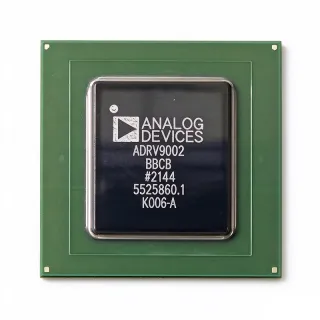
ADRV9002BBCZ - Dual RF Transceiver 30MHz-6GHz | Analog Devices
MPN: ADRV9002BBCZ ✓ Active| Qty | Unit Price | Extended |
|---|---|---|
| 1 | $281.68 | $281.68 |
| 10 | $265 | $2,650.00 |
| 100 | $245 | $24,500.00 |
| 500 | $225 | $112,500.00 |
| 1,000 | $210 | $210,000.00 |
ADRV9002BBCZ Overview
An RF transceiver is a device that combines both a transmitter and a receiver in a single package, enabling bidirectional communication over a radio frequency link. The ADRV9002 is a high-performance, highly linear, high dynamic range transceiver, making it suitable for demanding applications such as software-defined radio (SDR), 5G NR, and military communications. It supports both narrowband and wideband operation, offering flexibility for various system architectures.
Key features include dual-channel operation, frequency coverage from 30 MHz to 6 GHz, and integrated digital signal processing. The device provides excellent linearity and dynamic range, essential for modern communication systems. It operates over a temperature range of -40°C to +110°C, ensuring reliability in harsh environments. The package is a 196-TFBGA, CSPBGA, with a supplier device package of 196-CSPBGA (12x12).
The ADRV9002 utilizes advanced RF CMOS technology, integrating multiple functions that traditionally required discrete components. This integration reduces board space, power consumption, and system cost. The device includes on-chip synthesizers and digital filtering, simplifying the design of RF front-ends. Its high dynamic range enables it to handle weak signals in the presence of strong interferers, a critical requirement in crowded spectrum environments.
Typical applications include software-defined radio, 5G NR base stations, point-to-point microwave links, and military communications. The wide frequency range and dual-channel capability make it ideal for MIMO and diversity systems. The device is also suitable for test and measurement equipment, where precise RF signal generation and analysis are required.
When designing with the ADRV9002, careful attention must be paid to power supply decoupling and thermal management. The device's power dissipation is significant, and proper PCB layout with adequate ground planes and thermal vias is essential. The evaluation board EVAL-ADRV9002 provides a reference design for optimal performance.
Drop-in alternatives for ADRV9002BBCZ — same package, pin-to-pin compatible. Different-package parts requiring PCB rework are excluded.
Variants in this series
Same-series models that are drop-in compatible with ADRV9002BBCZ (same form factor and footprint) — differing in Package, Frequency Range, Supply Voltage, Interface, Type.
Quick Comparison Tool — Select alternative parts for side-by-side comparison:
ADRV9002BBCZ-RL
✅ Drop-In📋 Reference alternative (not in catalog)
ADRV9001BBCZ
⚡ Same Package ⚠️ Specs Unverified📋 Reference alternative (not in catalog)
AD9371BBCZ
⚡ Same Package ⚠️ Specs Unverified✓ In Stock
$147 / Unit
View Datasheet →ADRV9002BBCZ-REEL
✅ Drop-In✓ In Stock
$590.625 / Unit
View Datasheet →ADRV9002BBCZ-REEL7
✅ Drop-In📋 Reference alternative (not in catalog)
ADRV9002BBCZ Specifications
| Type | TxRx Only |
| Frequency Range | 30MHz ~ 6GHz |
| Number of Channels | 2 Tx, 2 Rx |
| Package / Case | 196-TFBGA, CSPBGA |
| Supplier Device Package | 196-CSPBGA (12x12) |
| Operating Temperature | -40°C ~ 110°C |
| MSL Level | 3 (168 Hours) |
| Package Type | Tray |
| Product Status | Active |
| Mounting Type | Surface Mount |
| RF Type | General Purpose |
ADRV9002BBCZ Pin Configuration
| Pin A1 | GND — Ground |
| Pin A2 | VDD — Power supply |
| Pin A3 | TX1_P — Transmit channel 1 positive |
| Pin A4 | TX1_N — Transmit channel 1 negative |
| Pin A5 | TX2_P — Transmit channel 2 positive |
| Pin A6 | TX2_N — Transmit channel 2 negative |
| Pin B1 | RX1_P — Receive channel 1 positive |
| Pin B2 | RX1_N — Receive channel 1 negative |
| Pin B3 | RX2_P — Receive channel 2 positive |
| Pin B4 | RX2_N — Receive channel 2 negative |
| Pin C1 | CLK_IN — Reference clock input |
| Pin C2 | SPI_CS — SPI chip select |
| Pin C3 | SPI_CLK — SPI clock |
| Pin C4 | SPI_SDIO — SPI data |
Typical Applications
ADRV9002BBCZ is suitable for 6 applications: Software-Defined Radio (SDR), 5G NR Base Stations, Point-to-Point Microwave Links, Military Communications, Test and Measurement Equipment, IoT and Smart Grid.
Software-Defined Radio (SDR)
The ADRV9002BBCZ is ideal for SDR platforms due to its wide frequency range (30 MHz to 6 GHz) and dual-channel capability. It enables flexible, reconfigurable radios that can operate across multiple bands and standards. Its high dynamic range allows reception of weak signals in congested spectrum, while the integrated DSP reduces external processing requirements. Designers can use the EVAL-ADRV9002 board for rapid prototyping.
Recommended
5G NR Base Stations
The ADRV9002BBCZ supports 5G NR applications with its dual-channel architecture, enabling MIMO and diversity schemes. Its frequency coverage up to 6 GHz covers key 5G bands, and its high linearity ensures compliance with stringent spectral masks. The integrated synthesizers simplify LO generation, reducing component count. The device's wide bandwidth and dynamic range make it suitable for both sub-6 GHz macro and small cell deployments.
Recommended
Point-to-Point Microwave Links
For microwave backhaul, the ADRV9002BBCZ provides dual-channel operation for frequency diversity and increased capacity. Its frequency range up to 6 GHz covers common microwave bands, and its high dynamic range ensures reliable links in fading conditions. The integrated DSP supports adaptive modulation and equalization. The compact CSPBGA package allows for dense integration in outdoor units.
Recommended
Military Communications
The ADRV9002BBCZ is suitable for military communications due to its wide frequency range and robust performance. It supports frequency hopping and secure waveforms with its fast synthesizer settling time. The device's high linearity and dynamic range are critical for anti-jamming and low probability of intercept. Its operating temperature range of -40°C to +110°C ensures operation in harsh environments.
Recommended
Test and Measurement Equipment
In test and measurement, the ADRV9002BBCZ can be used in signal generators, spectrum analyzers, and channel emulators. Its wide frequency range and dual-channel capability allow for simultaneous signal generation and analysis. The integrated DSP enables precise modulation and demodulation. The device's high dynamic range is essential for accurate measurements of weak signals.
Recommended
IoT and Smart Grid
For IoT and smart grid applications, the ADRV9002BBCZ provides reliable wireless connectivity over a wide frequency range. Its dual-channel capability supports diversity for improved link reliability. The device's low power consumption and small footprint make it suitable for edge devices. It can operate in sub-GHz bands for long-range, low-power communication.
Recommended
Recommended Products Summary
Engineering reference data for ADRV9002BBCZ — comparison, design guidance, and compliance information.
Selection Guide
Comparison with Alternatives
| Parameter | This Product | ADRV9002BBCZ-RL | ADRV9001BBCZ | AD9371BBCZ |
|---|---|---|---|---|
| Package | 196-CSPBGA (12x12) | 196-CSPBGA (12x12) | 196-CSPBGA (12x12) | 196-CSPBGA (12x12) |
| Brand | Analog Devices | Analog Devices | Analog Devices | Analog Devices |
| Frequency Range | 30 MHz to 6 GHz | 30 MHz to 6 GHz | 30 MHz to 6 GHz | 300 MHz to 6 GHz |
| Number of Channels | 2 Tx, 2 Rx | 2 Tx, 2 Rx | 1 Tx, 1 Rx | 2 Tx, 2 Rx |
| Operating Temperature | -40°C to +110°C | -40°C to +110°C | -40°C to +110°C | -40°C to +85°C |
| Package Type | Tray | Tape & Reel | Tray | Tray |
| MSL Level | 3 (168 Hours) | 3 (168 Hours) | 3 (168 Hours) | 3 (168 Hours) |
Key Differentiators
- Wide frequency range from 30 MHz to 6 GHz (vs AD9371BBCZ)
- Dual-channel capability (vs ADRV9001BBCZ)
- High dynamic range and linearity (vs AD9361BBCZ)
Design Notes
The ADRV9002BBCZ requires multiple power supply rails. Use low-noise LDOs for analog and digital supplies to minimize noise coupling into the RF path. Decouple each supply pin with 100nF and 10uF capacitors placed close to the pins. Refer to the datasheet for recommended supply sequencing.
For optimal RF performance, use a 4-layer or more PCB with a solid ground plane. Place the transceiver on a dedicated ground island and connect it to the main ground via multiple vias. Ensure controlled impedance for RF traces (e.g., 50 ohms) and keep them as short as possible. Follow the layout guidelines in the EVAL-ADRV9002 board design.
The ADRV9002BBCZ can dissipate significant power, especially during transmit. The package thermal resistance is specified per JEDEC JESD51-12. Use thermal vias under the exposed pad to conduct heat to the PCB ground plane. For high-power operation, consider adding a heatsink or forced air cooling. Monitor junction temperature to stay within limits.
Compliance Information
RoHS compliance is indicated by distributor listings. Other compliance data not specified in the provided data.