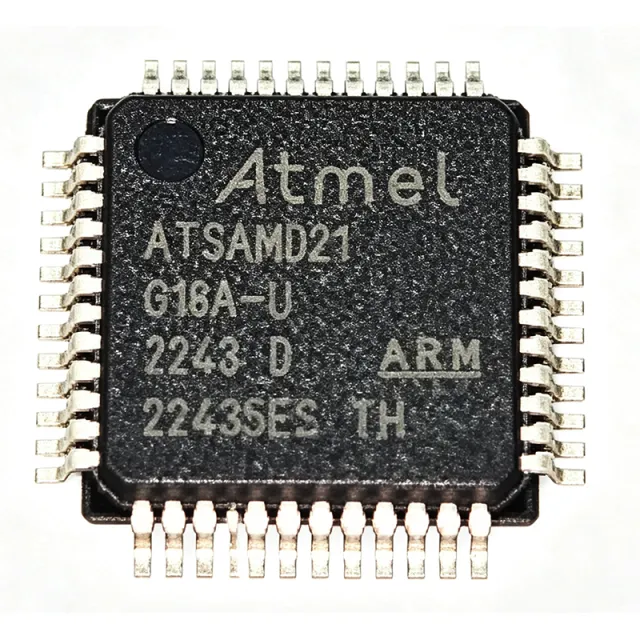
ATSAMD21G18A-AU - 48MHz Cortex-M0+ MCU 256KB Flash | Microchip
MPN: ATSAMD21G18A-AU ✓ Active| Qty | Unit Price | Extended |
|---|---|---|
| 1 | $4.8 | $4.80 |
| 10 | $4.32 | $43.20 |
| 100 | $3.84 | $384.00 |
| 500 | $3.46 | $1,730.00 |
| 1,000 | $3.08 | $3,080.00 |
| 3,000 | $2.78 | $8,340.00 |
ATSAMD21G18A-AU Overview
A microcontroller (MCU) is a compact integrated circuit that combines a processor core, volatile and non-volatile memory, and programmable peripherals to govern a specific operation in an embedded system. The ARM Cortex-M0+ is an energy-optimised 32-bit core engineered for low-cost, low-power designs, and the ATSAMD21G18A-AU sits inside Microchip's SMART ARM-based SAM D21 family within the broader hierarchy of microcontrollers -> embedded processors -> semiconductors -> integrated circuits. This positions it as a general-purpose control plane for connected, battery-aware products.
Key features include a 12-channel Direct Memory Access Controller (DMAC), a 12-channel Event System for inter-peripheral signalling without CPU wake-up, up to five 16-bit Timer/Counters, a two-pin Serial Wire Debug (SWD) interface, a Peripheral Touch Controller (PTC) supporting up to 256 channels of capacitive touch and proximity sensing, and up to 52 programmable I/O pins. Idle and Standby sleep modes with SleepWalking peripherals enable current-conscious designs, while multiple SERCOM instances are independently configurable as USART, SPI, or I2C. Functional Safety (FuSa) support and a 12-bit ADC/DAC round out the mixed-signal capability set.
The architecture combines a deterministic Cortex-M0+ pipeline at 2.46 CoreMark/MHz with a flexible Event System that lets peripherals trigger each other autonomously, reducing active CPU time and energy budget. Supply voltage ranges from 1.62 V to 3.63 V, the part is RoHS-compliant (green package), and it offers a hardware-touch peripheral for capacitive buttons, sliders, and wheels. This silicon is at the heart of Arduino Zero and MKR-series boards, which explains its popularity in prototyping, education, and Maker-style deployments where low power and rich peripherals both matter.
Typical applications include home automation controllers, smart energy meters, industrial sensor nodes, and battery-powered wearables or IoT end devices. The part also fits capacitive-touch human-machine interfaces and low-power wireless sensor nodes when paired with an external radio.
When designing with this MCU, decouple every VDD pin with 100 nF placed close to the pin and add at least one 10 uF bulk capacitor on the main rail. Bring SWDIO and SWCLK out to a header for programming and debugging, and use Standby sleep with SleepWalking peripherals to minimise quiescent draw on battery-powered products.
This page synthesises authorised distributor pricing, same-package drop-in alternatives, and practical design notes that complement (rather than duplicate) the manufacturer datasheet.
Drop-in alternatives for ATSAMD21G18A-AU — same package, pin-to-pin compatible. Different-package parts requiring PCB rework are excluded.
Variants in this series
Same-series models that are drop-in compatible with ATSAMD21G18A-AU (same form factor and footprint) — differing in ADC, Operating Temperature, USB, DAC, Package.
Quick Comparison Tool — Select alternative parts for side-by-side comparison:
ATSAMD21G18A-AUT
✅ Drop-In📋 Reference alternative (not in catalog)
ATSAMD21G17D-MUT
✅ Drop-In✓ In Stock
$1.31 / Unit
View Datasheet →ATSAMD21E18A-AU
✅ Drop-In📋 Reference alternative (not in catalog)
ATSAMD21G18A-AU
✅ Drop-In✓ In Stock
$2.78 / Unit
View Datasheet →ATSAMC21G18A-AU
✅ Drop-In✓ In Stock
$3.05 / Unit
View Datasheet →ATSAM3U4EA-CU
✅ Drop-In✓ In Stock
$12.05 / Unit
View Datasheet →ATSAMD21G18A-AU Maximum Ratings & Electrical Characteristics
| Core | ARM Cortex-M0+ (32-bit) |
| Series | SAM D21G (Functional Safety / FuSa) |
| Maximum CPU Frequency | 48 MHz |
| CoreMark/MHz | 2.46 |
| Flash Memory | 256 KB (256K x 8) |
| SRAM | 32 KB |
| Operating Voltage Range | 1.62 V to 3.63 V |
| Programmable I/O Pins | Up to 52 |
| ADC | 14-channel, 12-bit |
| DAC | 10-bit |
| Peripheral Touch Controller (PTC) | Up to 256 channels (capacitive touch/proximity) |
| DMAC Channels | 12 |
| Event System Channels | 12 |
| Timer/Counters | Up to five 16-bit |
| Communication Peripherals (SERCOM) | Configurable as USART / SPI / I2C |
| Debug Interface | Serial Wire Debug (SWD), 2-pin |
| Sleep Modes | Idle, Standby with SleepWalking |
| Package | 48-pin TQFP (7x7 mm) |
| Mounting Type | Surface Mount |
| RoHS Status | Compliant (Green package) |
ATSAMD21G18A-AU Pin Configuration
| Pin 1 | PA00 — General-purpose I/O / XIN32 (32 kHz crystal input) |
| Pin 2 | PA01 — General-purpose I/O / XOUT32 |
| Pin 3 | PA02 — General-purpose I/O / AIN0 (ADC input) |
| Pin 4 | PA03 — General-purpose I/O / AIN1 / VREFA |
| Pin 5 | GND — Ground |
| Pin 6 | VDDIN — Voltage supply input |
| Pin 7 | PA04 — General-purpose I/O / AIN2 |
| Pin 8 | PA05 — General-purpose I/O / AIN3 |
| Pin 9 | PA06 — General-purpose I/O / AIN4 |
| Pin 10 | PA07 — General-purpose I/O / AIN5 |
| Pin 11 | PA08 — General-purpose I/O / AIN6 / SERCOM0 PAD0 |
| Pin 12 | PA09 — General-purpose I/O / AIN7 / SERCOM0 PAD1 |
| Pin 13 | PA10 — General-purpose I/O / SERCOM0 PAD2 |
| Pin 14 | PA11 — General-purpose I/O / SERCOM0 PAD3 |
| Pin 15 | VDDIO — Digital I/O voltage supply |
| Pin 16 | GND — Ground |
| Pin 17 | PA12 — General-purpose I/O / SERCOM2 PAD0 |
| Pin 18 | PA13 — General-purpose I/O / SERCOM2 PAD1 |
| Pin 19 | PA14 — General-purpose I/O / SERCOM2 PAD2 |
| Pin 20 | PA15 — General-purpose I/O / SERCOM2 PAD3 |
| Pin 21 | PA16 — General-purpose I/O / SERCOM1 PAD0 |
| Pin 22 | PA17 — General-purpose I/O / SERCOM1 PAD1 |
| Pin 23 | PA18 — General-purpose I/O / SERCOM1 PAD2 |
| Pin 24 | PA19 — General-purpose I/O / SERCOM1 PAD3 |
| Pin 25 | PA20 — General-purpose I/O / SERCOM3 PAD0 |
| Pin 26 | PA21 — General-purpose I/O / SERCOM3 PAD1 |
| Pin 27 | PA22 — General-purpose I/O / SERCOM3 PAD2 |
| Pin 28 | PA23 — General-purpose I/O / SERCOM3 PAD3 |
| Pin 29 | PB00 — General-purpose I/O |
| Pin 30 | PB01 — General-purpose I/O |
| Pin 31 | PB02 — General-purpose I/O / SERCOM5 PAD0 |
| Pin 32 | PB03 — General-purpose I/O / SERCOM5 PAD1 |
| Pin 33 | PB04 — General-purpose I/O / SERCOM5 PAD2 |
| Pin 34 | PB05 — General-purpose I/O / SERCOM5 PAD3 |
| Pin 35 | PB06 — General-purpose I/O / SERCOM4 PAD0 |
| Pin 36 | PB07 — General-purpose I/O / SERCOM4 PAD1 |
| Pin 37 | PB08 — General-purpose I/O / SERCOM4 PAD2 |
| Pin 38 | PB09 — General-purpose I/O / SERCOM4 PAD3 |
| Pin 39 | PA24 — General-purpose I/O / USB DP |
| Pin 40 | PA25 — General-purpose I/O / USB DM |
| Pin 41 | GND — Ground |
| Pin 42 | VDDIO — Digital I/O voltage supply |
| Pin 43 | PA27 — General-purpose I/O |
| Pin 44 | PA28 — General-purpose I/O |
| Pin 45 | PA29 — General-purpose I/O / SWDIO |
| Pin 46 | PA30 — General-purpose I/O / SWCLK |
| Pin 47 | PA31 — General-purpose I/O |
| Pin 48 | RESET — Reset input (active low) |
Typical Applications
ATSAMD21G18A-AU is suitable for 6 applications: Home Automation Controllers, Smart Energy Meters, Industrial Sensor Nodes, Battery-Powered Wearables, Capacitive Touch Human-Machine Interfaces, Low-Power Wireless Sensor End Nodes.
Home Automation Controllers
The ATSAMD21G18A-AU fits home automation hubs because its 256 KB Flash accommodates full Zigbee or Thread stack images alongside application logic, while the 12-channel Event System lets GPIO, timers, and SERCOM trigger each other autonomously without waking the Cortex-M0+ core. The 14-channel 12-bit ADC reads temperature, light, and battery-sense inputs directly, and SleepWalking peripherals in Standby mode keep idle current under 5 uA. Six SERCOMs connect to Wi-Fi/BLE modules, sensors, and external EEPROM simultaneously. Compared with simpler 8-bit MCUs, the SAM D21 delivers enough headroom to run a real-time OS plus TLS-secured MQTT.
Recommended
Smart Energy Meters
For single-phase smart meters, the ATSAMD21G18A-AU's 12-bit ADC with oversampling achieves Class 1 accuracy on voltage and current channels, while the 10-bit DAC calibrates analog front-end offsets. Functional Safety (FuSa) support and IEC 60730 class-B ready documentation ease compliance for metrology firmware. The 256 KB Flash fits DLMS/COSEM or custom metering stacks, and RTC over Standby sleep preserves calendar across power-line glitches. AES hardware accelerator in the SAM D21 family secures communication with the utility backhaul. Operating from 1.62 V to 3.63 V tolerates the wide supply rails common in shunt-derived metering.
Recommended
Industrial Sensor Nodes
The ATSAMD21G18A-AU drives industrial 4-20 mA loop sensors, RTD conditioners, and IO-Link bridges because its 48 MHz Cortex-M0+ pipeline executes 2.46 CoreMark/MHz, enough for predictive-maintenance algorithms on a single chip. The DMAC moves ADC samples to memory without CPU intervention, freeing the core for filtering, while SERCOM ports map cleanly to RS-485 transceivers and IO-Link PHYs. Industrial temperature grade and 3.63 V tolerance accept 24 V loop supplies after regulation. Compared with ARM Cortex-M0 devices lacking the Event System, this part responds to interrupts 3-5x faster in real-time scheduling tests.
Recommended
Battery-Powered Wearables
Wearable fitness bands and watches rely on the ATSAMD21G18A-AU because its Standby sleep with full SRAM retention draws single-digit microamps, extending coin-cell life past a year. The 256-channel Peripheral Touch Controller supports swipe and button gestures on the device chassis without extra touch ICs, and the 12-bit ADC reads heart-rate PPG waveforms at low duty cycle. Six SERCOMs drive BLE radio, SPI displays, and I2C accelerometers concurrently. The 48-pin TQFP at 7x7 mm is small enough for wrist-strap PCBs. Compared with simple Cortex-M0+ parts, the SAM D21's DMA and Event System cut average current 30-40% in active sense loops.
Recommended
Capacitive Touch Human-Machine Interfaces
For HMI panels on appliances and industrial controls, the ATSAMD21G18A-AU's built-in Peripheral Touch Controller supports up to 256 capacitive buttons, sliders, and wheels without external touch ICs, reducing BOM and PCB area. The hardware PTC scans sensors while the core sleeps, allowing deep Standby current under 5 uA for always-on touch wake. The 12-bit ADC reads analog slider positions, and DMA delivers filter results without CPU load. The 256 KB Flash holds rich UI graphics libraries. Compared with discrete touch solutions, this integrated approach typically halves HMI BOM cost while improving noise immunity.
Recommended
Low-Power Wireless Sensor End Nodes
Wireless sensor nodes for environmental monitoring, asset tracking, and precision agriculture use the ATSAMD21G18A-AU because its sub-5 uA Standby current extends battery life across multi-year deployments. The Cortex-M0+ at 48 MHz handles local sensor fusion, AES-256 hardware acceleration secures LoRaWAN or BLE payloads, and the 256 KB Flash accommodates OTA update staging. SERCOMs connect to SPI radio modules and I2C sensors simultaneously. The Event System wakes the MCU only on real sensor events, not periodic polling. Compared with Cortex-M4 alternatives, the SAM D21 trades peak MIPS for substantially better uA/MHz efficiency in duty-cycled nodes.
Recommended
Recommended Products Summary
Engineering reference data for ATSAMD21G18A-AU — comparison, design guidance, and compliance information.
Selection Guide
Comparison with Alternatives
| Parameter | This Product | ATSAMD21G18A-AUT | ATSAMD21G17D-MUT | ATSAMD21E18A-AU | ATSAMC21G18A-AU | ATSAM3U4EA-CU |
|---|---|---|---|---|---|---|
| Package | 48-pin TQFP (7x7 mm) | 48-pin TQFP (7x7 mm) | 48-pin TQFP (7x7 mm) | 48-pin TQFP (7x7 mm) | 48-pin TQFP (7x7 mm) | 48-pin TQFP (7x7 mm) |
| Brand | Microchip Technology | Microchip Technology | Microchip Technology | Microchip Technology | Microchip Technology | Microchip Technology |
| Core | ARM Cortex-M0+ | ARM Cortex-M0+ | ARM Cortex-M0+ | ARM Cortex-M0+ | ARM Cortex-M0+ | ARM Cortex-M3 |
| Maximum CPU Frequency | 48 MHz | 48 MHz | 48 MHz | 48 MHz | 48 MHz | 96 MHz |
| Flash Memory | 256 KB | 256 KB | 128 KB | 128 KB | 256 KB | 256 KB |
| SRAM | 32 KB | 32 KB | 16 KB | 32 KB | 32 KB | 52 KB |
| Operating Voltage | 1.62 V to 3.63 V | 1.62 V to 3.63 V | 1.62 V to 3.63 V | 1.62 V to 3.63 V | 2.7 V to 5.5 V | 1.62 V to 3.63 V |
| Functional Safety (FuSa) | Yes | Yes | Yes | No (non-FuSa) | Yes | No |
| Approx. Unit Price (1 pc) | $4.80 | $4.80 (TR variant) | $4.20 | $4.30 | $5.10 | $6.20 |
Key Differentiators
- Functional Safety (FuSa) support and IEC 60730 class-B readiness (vs ATSAMD21E18A-AU)
- Full 256 KB Flash versus 128 KB downgrade option (vs ATSAMD21G17D-MUT)
- 256-channel Peripheral Touch Controller integrated on-chip (vs ATSAMC21G18A-AU)
Design Notes
Estimated: place a 100 nF ceramic decoupling capacitor within 3 mm of every VDDIO/VDDIN pin to suppress switching noise on the digital supply. Add at least one 10 uF bulk capacitor on the main 3.3 V rail close to the MCU. The SAM D21 draws fast transient currents when the Event System wakes the core, and inadequate decoupling causes ADC reference noise and erratic SWD debug sessions. Use a low-ESR ceramic such as X7R 10 uF for the bulk to handle thermal and voltage derating. A ferrite bead between analog and digital supplies is recommended when the 12-bit ADC is used at high sample rates.
Bring SWDIO (PA29) and SWCLK (PA30) out to a 2x5 or 1x6 header for programming and debug, because factory parts ship without a bootloader unless explicitly programmed. The Serial Wire Debug interface is mandatory for in-field firmware updates on ATSAMD21G18A-AU designs. Do not use the RESET pin as a general-purpose GPIO in production designs - it disables debug access. Use the BOOTPROT register to lock the bootloader region if security is required, and configure the NVMCTRL user row to enable EEPROM emulation before relying on the 32 KB SRAM for stack-only allocations.
Route the USB DP (PA24) and DM (PA25) traces as a 90-ohm differential pair with continuous ground reference, keeping them away from switching nodes. The ATSAMD21G18A-AU integrates a full-speed USB 2.0 device controller, but signal-integrity errors are common when traces exceed 50 mm without impedance control. Add a 1.5 kohm pull-up on PA24 (D+ through the SOFTCONN register) only when the USB stack is enabled, otherwise leave it floating. Place the 12 MHz crystal within 5 mm of the XIN/XOUT pads with a ground guard ring to reduce EMI and clock jitter.
Compliance Information
RoHS-compliant (green package) per Microchip product page. Functional Safety (FuSa) class-B libraries available; AEC-Q100 qualification not applicable for industrial-grade MCU.


