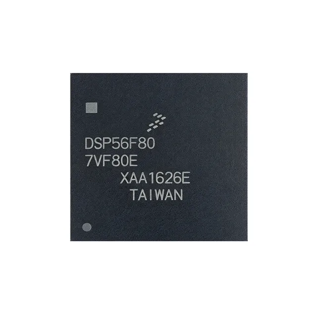
DSP56F807VF80E - 16-bit 56800 DSC 80MHz 160-MAPBGA | NXP
MPN: DSP56F807VF80E ✗ End of Life| Qty | Unit Price | Extended |
|---|---|---|
| 1 | $42.1875 | $42.19 |
| 10 | $30.4688 | $304.69 |
| 100 | $26.9531 | $2,695.31 |
| 500 | $25.7813 | $12,890.65 |
| 1,000 | $24.6094 | $24,609.40 |
DSP56F807VF80E Overview
A Digital Signal Controller is a hybrid of a digital signal processor and a microcontroller: like a DSP it executes multiply-accumulate intensive control loops fast, and like an MCU it integrates flash memory, timers, communication interfaces, and ADCs for standalone embedded operation. In the semiconductor hierarchy, the DSP56F807VF80E sits within the digital signal controller category, under the broader families of digital signal processors, microcontrollers, and embedded processors.
Key features include the Harvard-style 56800 architecture executing a 16-bit fixed-point instruction set with DSP addressing modes, up to 80 MHz core frequency for deterministic single-cycle MAC operations, 120KB of program flash, and support for up to 64K x 16-bit words (128KB) each of external program and data memory expansion per the manufacturer datasheet. The 3.3V supply domain and dense 160-ball MAPBGA footprint suit compact motor-control boards where board area is constrained.
Architecturally, the 56800 core pairs a Harvard memory organization with microcontroller-friendly instruction set extensions, allowing C-compiled control code and hand-optimized DSP kernels to coexist. On-chip peripherals target servo and industrial drive topologies: PWM generation, analog-to-digital conversion, and serial communication, all synchronized to the 80 MHz core clock for low-latency current-loop control.
Typical applications include servo motor control, industrial power inverters and converters, and digital power supplies, where the single-chip integration of DSP math and MCU peripherals reduces bill-of-materials cost versus a separate DSP-plus-MCU pairing.
Design consideration: this part is End-of-Life per the NXP product page, so new designs should evaluate migration to the MC56F8xx successor family, and existing designs should secure last-time-buy inventory.
This page synthesizes distributor pricing, datasheet references, EOL status, and replacement-strategy analysis not consolidated in the manufacturer datasheet.
Drop-in alternatives for DSP56F807VF80E — same package, pin-to-pin compatible. Different-package parts requiring PCB rework are excluded.
Variants in this series
Same-series models that are drop-in compatible with DSP56F807VF80E (same form factor and footprint) — differing in Core Architecture, Package, Program Flash Memory, Maximum Clock Frequency, Core.
Quick Comparison Tool — Select alternative parts for side-by-side comparison:
No drop-in alternatives available for this product.
Request AlternativesDSP56F807VF80E Specifications
| Core | 56800 |
| Core Architecture | 16-bit Harvard-style DSC (DSP + MCU) |
| Maximum Clock Frequency | 80 MHz |
| Program Flash Memory | 120KB (60K x 16-bit) |
| External Memory Expansion | Up to 64K x 16-bit words (128KB) each program and data |
| Supply Voltage | 3.3 V |
| Package | 160-MAPBGA (15 x 15 mm) |
| Mounting Type | Surface Mount |
| Product Family | 56800 / 56F8xx Digital Signal Controllers |
| Application Targeting | Servo and motor control, power inverter and converter |
| Lifecycle Status | End of Life (per NXP product page) |
| Unit Price (qty 1, LCSC) | 32.6123 USD as of 2026-10-10 |
DSP56F807VF80E 160-mapbga (15 x 15 mm) Pin Configuration Guide
Pin configuration for DSP56F807VF80E (160-mapbga (15 x 15 mm) package). Pin numbering, functions, and connection diagrams are defined in the manufacturer datasheet. Refer to it for the exact footprint and soldering guidelines.

No detailed pinout data available for DSP56F807VF80E.
Refer to the datasheet for full pin configuration.
Typical Applications
DSP56F807VF80E is suitable for 6 applications: Servo Motor Control, Power Inverters, Power Converters, Industrial Automation, Digital Power Supplies, Legacy Embedded System Maintenance.
Servo Motor Control
The DSP56F807VF80E was designed explicitly for servo and motor control, per the NXP product page which names servo control as a primary application. The 56800 core at 80 MHz executes single-cycle multiply-accumulate operations, enabling fast field-oriented control current loops, while the integrated 16-bit DSC peripherals handle PWM generation and ADC feedback sampling in a single chip. Using one DSC instead of a separate DSP plus MCU pairing reduces BOM cost and control-loop latency because the same core services both the fast control math and the communication housekeeping. Engineers implementing servo drives on this part should budget the 80 MHz core across current loop, position loop, and supervisory tasks, and note that End-of-Life status means new servo designs should target the MC56F8xx successor family while existing designs secure last-time-buy inventory.
Recommended
Power Inverters
Digital power inverters benefit directly from the DSP56F807VF80E's architecture: the NXP product page explicitly lists power inverter applications as a core use case for the 56F807. The 80 MHz Harvard-style 56800 core performs the sinusoidal modulation and feedback math with deterministic timing, while integrated peripherals generate PWM gate-drive sequences synchronized to the ADC conversion of output current and voltage. The 3.3V supply domain and 160-ball MAPBGA (15x15 mm) package allow compact controller placement on crowded inverter control boards. Because the single-chip solution replaces a discrete DSP-plus-MCU combination, designers gain cost and board-area savings. Note that the part is End-of-Life: inverter designs in production should execute last-time buys, and new designs should evaluate MC56F8xx parts with equivalent PWM and ADC subsystems.
Recommended
Power Converters
The 56F807 is cited by NXP as a cost-effective solution for power converter applications alongside inverters and servo drives. In AC-DC and DC-DC converter control, the DSP56F807VF80E's 80 MHz core sustains the high-frequency compensation loops and power-factor-correction math with single-cycle MAC throughput, while on-chip ADC channels sample the converter's output and current-shunt signals. The Harvard-style architecture keeps program fetches from the 120KB flash independent of data accesses, preserving deterministic loop timing that is essential for stable converter regulation at elevated switching frequencies. The 160-ball MAPBGA footprint integrates the controller into dense power boards. Designers should also use the external memory interface, which supports up to 128KB each of program and data memory, when converter firmware includes large compensation tables.
Recommended
Industrial Automation
Industrial automation nodes that combine real-time control with communication fit the DSP56F807VF80E's hybrid DSP-plus-MCU design philosophy. The 56800 core executes a C-compiled MCU workload alongside optimized DSP kernels, so a single device can run a motion loop, sequence I/O, and service serial links without external processors. The 120KB on-chip program flash supports substantial application firmware, and the external memory interface (up to 64K x 16-bit words, 128KB each program and data per the NXP datasheet) accommodates larger table-driven automation logic. The 3.3V I/O domain integrates with standard industrial logic levels. Given the confirmed End-of-Life status on the NXP product page, automation equipment makers should plan migration to the MC56F8xx family and audit spare-part inventories for field-deployed controllers.
Recommended
Digital Power Supplies
Digitally controlled power supplies require fast, deterministic feedback loops that the DSP56F807VF80E serves well. The 80 MHz 56800 core computes voltage-mode and current-mode control updates with single-cycle multiply-accumulate throughput, while the integrated ADC and PWM peripherals close the loop on-chip, minimizing sensor-to-PWM latency compared with external controller pairings. The NXP datasheet positions the 56F807 family around this class of control-intensive application. The 3.3V, 16-bit architecture also simplifies interfacing with supervisory logic in rack-mounted supplies. Because the part is now EOL with no direct replacements listed by NXP, new digital supply platforms should begin on the MC56F8xx family, which retains a similar DSC programming model to ease firmware porting, while existing supply designs execute last-time buys of the 160-MAPBGA part.
Recommended
Legacy Embedded System Maintenance
A significant ongoing use case for the DSP56F807VF80E is sustaining fielded legacy systems: NXP community threads from February 2026 document customers actively seeking replacement strategies after receiving EOL notices for this exact MPN. Maintenance engineers should verify remaining distributor stock (LCSC, DigiKey, Mouser list the part as of 2026-10-10, with LCSC at $32.6123 for qty 1), then execute last-time-buy quantities sized to the product's remaining service life. Firmware archives, development toolchains, and programming fixtures for the 56800 core should be preserved, since future board repairs will need them. For long-lived equipment where board redesign is impractical, broker channels and factory excess inventory are the primary long-term sourcing routes after authorized stock depletes.
Recommended
Recommended Products Summary
Engineering reference data for DSP56F807VF80E — comparison, design guidance, and compliance information.
Selection Guide
Comparison with Alternatives
| Parameter | This Product |
|---|---|
| Package | 160-MAPBGA (15x15 mm) |
| Brand | NXP Semiconductors |
| Core | 56800 (16-bit DSC) |
| Max Clock Frequency | 80 MHz |
| Program Flash | 120KB (60K x 16) |
| Supply Voltage | 3.3 V |
| External Memory Support | 64K x 16 (128KB) each program/data |
| Lifecycle Status | End of Life |
Key Differentiators
- Single-chip DSP-plus-MCU integration for cost-sensitive drives (vs DSP56321VF240)
- Expanded external memory headroom (vs Small-flash DSC alternatives)
- Established but EOL: plan migration deliberately (vs MC56F8357VVFE)
Design Notes
The DSP56F807VF80E is End-of-Life per the official NXP product page, and NXP confirmed in community threads (February 2026) that no direct replacements were listed in the discontinuance notice. Any new PCB design using this part is effectively designing in an obsolete component. For existing designs, calculate last-time-buy quantity from field-failure projections plus service-life spares before authorized distributor stock (LCSC, DigiKey, Mouser) is exhausted. Budget for price escalation: LCSC already lists $32.6123 for qty 1 as of 2026-10-10, and EOL pricing typically rises as inventory depletes.
The DSP56F807VF80E operates from a 3.3V supply per the DigiKey and datasheets.com listings. Digital signal controllers switching at 80 MHz impose fast transient loads, so follow the NXP DSP56F807 datasheet power-supply recommendations for bulk and high-frequency decoupling at each BGA power ball. Because a 160-ball MAPBGA requires via-in-pad or fanout vias for power delivery, plan the power distribution network during the PCB stack-up stage, not after layout. Estimated: transient di/dt management is the dominant concern; verify with the datasheet's supply decoupling section.
The 160-ball MAPBGA in a 15x15 mm body uses approximately 0.8 mm ball pitch typical for this NXP MAPBGA family; verify the exact ball pitch against the mechanical drawing in the official NXP datasheet before committing to a footprint. The footprint is a redesign-level constraint: since no drop-in successor exists, any migration to the MC56F8xx family requires a new land pattern and BGA fanout. Escape routing on 4-layer boards is feasible with 0.1 mm trace/space through the two outer fanout rows; inner balls require microvias or via-in-pad on denser stack-ups.
The external memory interface supports up to 64K x 16-bit words (128KB) each of program and data memory per the NXP datasheet. When using external memory, treat the address and data bus as fast parallel buses: keep trace length matching across data lines, series-terminate address lines where the datasheet recommends, and route away from PWM and power-stage switching nodes typical of motor-control boards. Poor bus routing manifests as intermittent memory corruption that is difficult to diagnose on BGA-packaged parts where signal access for probing is limited.
Compliance Information
The 'E' suffix in the NXP ordering nomenclature conventionally indicates a pb-free/RoHS-compliant variant, but official compliance status must be verified on the NXP product page Environmental Quality section; not confirmed in provided web data.


