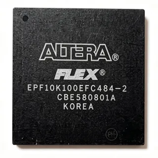
EP1AGX20CF484C6NGA - 20K LE Arria GX FPGA, 484-FBGA | Intel
MPN: EP1AGX20CF484C6NGA ✗ End of Life| Qty | Unit Price | Extended |
|---|---|---|
| 1 | $245 | $245.00 |
| 10 | $232.5 | $2,325.00 |
| 100 | $215 | $21,500.00 |
| 500 | $198.75 | $99,375.00 |
| 1,000 | $185 | $185,000.00 |
EP1AGX20CF484C6NGA Overview
An FPGA (Field Programmable Gate Array) is a semiconductor device built around an array of configurable logic blocks (CLBs), embedded memory blocks, DSP blocks, and programmable routing. FPGAs occupy the high-end of the programmable-logic hierarchy, sitting above CPLDs (smaller, non-volatile, lower-density) and below ASICs in performance-per-watt. The Arria GX family specifically targets cost-sensitive applications that still require transceivers, bridging the gap between Cyclone (no SERDES) and Stratix (high-end SERDES + DSP) within Intel's programmable-logic portfolio. The 'AGX' prefix denotes the Arria GX sub-family; '20' is the logic-density code.
Key features of the EP1AGX20CF484C6NGA include integrated transceivers supporting CPRI, PCI Express (Gen1), Gigabit Ethernet, Serial RapidIO, and SDI protocols; embedded multipliers and DSP blocks; phase-locked loops for clock management; and configuration via passive serial, fast passive parallel, JTAG, or Altera EPCS/EPCQ flash. The -6 speed grade is a mid-tier speed bin, balancing Fmax and power. The 484-FBGA package exposes 230 user I/O pins, leaving significant headroom for parallel interfaces such as DDR/DDR2 memory controllers and LVDS channels.
Architecturally, the Arria GX fabric combines 4-input LUT-based logic elements, M512/M4K/M-RAM memory blocks, MLABs, and dedicated 18x18 multipliers feeding hardened DSP blocks. The transceiver blocks (up to 8 in this device) integrate serializer/deserializer, clock-data recovery, and physical coding sublayer logic, offloading serial I/O entirely from the programmable fabric. Configuration is stored in SRAM cells, requiring a boot flash or JTAG controller for stand-alone operation.
Typical applications for the EP1AGX20CF484C6NGA include wireless baseband preprocessing, broadcast video routers and switchers, industrial imaging and machine vision, military radar and signal-intelligence front ends, and protocol-bridging cards for telecom backplanes. The device's combination of mid-density logic, embedded transceivers, and 230 I/O makes it well-suited to designs that must aggregate multiple legacy interfaces (parallel data, LVDS, SERDES) onto a single board.
When designing with the EP1AGX20CF484C6NGA, engineers should follow Intel's power-decoupling guidance for Arria GX, place the EPCS configuration flash within 4 inches of the FPGA, and observe the JTAG chain topology if multiple Intel devices share the bus. Transceiver channels require matched-length differential routing and AC-coupling capacitors per Intel's pin-out guidelines.
This page synthesizes distributor pricing, drop-in pin-compatible variants, and application engineering notes not found in the manufacturer datasheet. Engineers can use the comparison table to evaluate the EP1AGX20CF484C6NGA against other members of the Arria GX family when balancing logic capacity against package size.
Drop-in alternatives for EP1AGX20CF484C6NGA — same package, pin-to-pin compatible. Different-package parts requiring PCB rework are excluded.
Variants in this series
Same-series models that are drop-in compatible with EP1AGX20CF484C6NGA (same form factor and footprint) — differing in Speed Grade, Package, Transceivers, Family, Process Technology.
Quick Comparison Tool — Select alternative parts for side-by-side comparison:
EP1AGX20CF484C6N
✅ Drop-In✓ In Stock
$110 / Unit
View Datasheet →EP1AGX20CF484C6
✅ Drop-In✓ In Stock
$153.72 / Unit
View Datasheet →EP1AGX20CF484C3
✅ Drop-In✓ In Stock
$195 / Unit
View Datasheet →EP1AGX35CF484C6N
✅ Drop-In ⚠️ Specs Unverified✓ In Stock
$118 / Unit
View Datasheet →EP1AGX20CF484C6NGA Maximum Ratings & Electrical Characteristics
| Series | Arria GX |
| Family | Intel Arria GX FPGA |
| Logic Elements (LE) | 21,580 |
| Total RAM Bits | 1,229,184 |
| User I/O Pins | 230 |
| Package / Case | 484-FBGA (23x23 mm) |
| Supplier Device Package | 484-FBGA (23x23) |
| Core Voltage - Supply | 1.15 V to 1.25 V |
| Speed Grade | -6 |
| Mounting Type | Surface Mount |
| Configuration Method | SRAM, JTAG, EPCS flash |
| Transceivers | Up to 8 high-speed SERDES channels |
| Hardware Multipliers | Embedded 18x18 multipliers |
EP1AGX20CF484C6NGA 484-fbga (23x23) Pin Configuration Guide
Pin configuration for EP1AGX20CF484C6NGA (484-fbga (23x23) package). This digital IC includes GPIO, communication interfaces (UART, SPI, I2C), and power pins. Refer to the manufacturer datasheet for alternate pin functions and configuration options. Essential for embedded system design and PCB layout.

No detailed pinout data available for EP1AGX20CF484C6NGA.
Refer to the datasheet for full pin configuration.
Typical Applications
EP1AGX20CF484C6NGA is suitable for 6 applications: Wireless Baseband Preprocessing, Broadcast Video Routers and Switchers, Industrial Imaging and Machine Vision, Military Radar and SIGINT Front Ends, Telecom Protocol-Bridging Cards, Test and Measurement Instrumentation.
Wireless Baseband Preprocessing
The EP1AGX20CF484C6NGA fits wireless baseband preprocessing roles where mid-density fabric and integrated SERDES both matter. Its 21,580 logic elements plus embedded 18x18 multipliers and DSP blocks can run channelization, crest-factor reduction (CFR) and digital pre-distortion (DPD) for a remote-radio-head (RRH) signal chain. The device's high-speed transceivers handle CPRI or OBSAI links between baseband unit and radio unit at rates up to 3.125 Gbps per lane, removing the need for external PHY chips. With 230 user I/O pins, designers can fan out parallel LVDS samples to ADC/DAC, and the 1.15-1.25V core supply keeps power dissipation manageable in fan-cooled enclosures. Compared with pure-DSP ASICs, the Arria GX offers a reprogrammable platform for protocol upgrades without re-spinning the PCB.
Recommended
Broadcast Video Routers and Switchers
The EP1AGX20CF484C6NGA is well-suited to broadcast video routers and SDI switchers that aggregate multiple serial digital video streams. Its integrated transceivers natively support SD-SDI, HD-SDI, and 3G-SDI at 270 Mbps, 1.485 Gbps, and 2.97 Gbps respectively, eliminating external serializer/deserializer parts. The 21,580 logic elements plus 1,229,184 bits of RAM provide line-buffering and embedded audio de-embedding/processing inside one fabric, while the 230 user I/O pins accept parallel video, GPIOs, and control panel interfaces. The 484-FBGA package supports high-density BGA assembly and clean return-path layout critical for jitter-sensitive SDI signals. Designers benefit from a single-device bill of materials that replaces what previously required a SERDES IC plus a CPLD or ASIC glue layer.
Recommended
Industrial Imaging and Machine Vision
In industrial imaging and machine-vision applications, the EP1AGX20CF484C6NGA interfaces to Camera Link, CoaXPress, or GigE Vision cameras through its high-speed SERDES channels and parallel I/O. The 21,580 logic elements and embedded multipliers handle real-time image preprocessing - Bayer demosaicing, lens-shading correction, edge detection - while frame buffers map onto the 1,229,184 bits of M4K/M-RAM. The 230 user I/O accommodate 32-bit Camera Link base configuration plus GPIO for trigger and strobe lines. Designers benefit from the Arria GX's industrial temperature grade variants for factory-floor deployment, where ambient temperatures can reach +85C around enclosure walls. The 484-FBGA package allows a compact camera-side board with thermal vias under the die for heat dissipation.
Recommended
Military Radar and SIGINT Front Ends
Defense programs use the EP1AGX20CF484C6NGA in radar and signal-intelligence (SIGINT) front ends where mid-density logic plus transceivers compress board count. The fabric can run pulse compression, MTI filtering, or FFT pre-processing on ADC data while the SERDES streams digitized samples to a back-end processor via VITA-49 or Aurora. The device's tolerance of industrial temperature ranges makes it suitable for ruggedized enclosures on airborne and naval platforms, and the 484-FBGA package supports the high pin density required for multi-channel ADC/DAC fan-out. Engineers favor the Arria GX family because of its mature Quartus II tool chain, which is still actively maintained for defense customers with long program lifecycles despite the commercial part being NRND.
Recommended
Telecom Protocol-Bridging Cards
The EP1AGX20CF484C6NGA is a strong fit for protocol-bridging line cards that must convert between legacy telecom interfaces (T1/E1, T3/E3, LVDS) and modern packet fabrics (Ethernet, RapidIO). The integrated SERDES provide native RapidIO, PCI Express Gen1, and Gigabit Ethernet ports, while the 230 user I/O and 21,580 logic elements handle the framing, de-framing, and clock-domain crossing logic. Designers can implement a multi-protocol bridge on a single device, replacing what was previously two or three ASSPs. The 484-FBGA footprint exposes enough parallel I/O for inter-card backplane LVDS, and the device's tolerance of industrial temperature supports telco central-office deployments. This same architectural pattern translates to test-and-measurement equipment where multiple legacy bus protocols must be aggregated.
Recommended
Test and Measurement Instrumentation
Test and measurement instruments such as protocol analyzers, logic analyzers, and oscilloscope front ends use the EP1AGX20CF484C6NGA as a data-routing and trigger-correlation engine. The 21,580 logic elements allow dense FPGA-based state machines for trigger sequencing, while the 1,229,184 bits of RAM hold deep acquisition buffers before DMA transfer to host memory. The high-speed SERDES lanes capture serialized probe traffic at multi-gigabit rates without external PHYs, and the 230 user I/O accept parallel probe pods. The 484-FBGA package supports the dense mixed-signal layout required to keep analog and digital return paths short. Engineers can implement protocol-aware decoding (PCIe, SATA, USB, MIPI) on the same fabric, accelerating time-to-market for new protocol support.
Recommended
Recommended Products Summary
Engineering reference data for EP1AGX20CF484C6NGA — comparison, design guidance, and compliance information.
Selection Guide
Comparison with Alternatives
| Parameter | This Product | EP1AGX20CF484C6N | EP1AGX20CF484C6 | EP1AGX20CF484C3 | EP1AGX35CF484C6N |
|---|---|---|---|---|---|
| Brand | Intel | Intel | Intel | Intel | Intel |
| Package | 484-FBGA (23x23 mm) | 484-FBGA (23x23 mm) - same | 484-FBGA (23x23 mm) - same | 484-FBGA (23x23 mm) - same | 484-FBGA (23x23 mm) - same |
| Logic Elements | 21,580 | 21,580 | 21,580 | 21,580 | 33,200 |
| Total RAM Bits | 1,229,184 | 1,229,184 | 1,229,184 | 1,229,184 | 1,540,608 |
| User I/O Pins | 230 | 230 | 230 | 230 | 230 |
| Speed Grade | -6 | -6 | -6 | -3 (slower by ~15%) | -6 |
| Core Voltage | 1.15 V to 1.25 V | 1.15 V to 1.25 V | 1.15 V to 1.25 V | 1.15 V to 1.25 V | 1.15 V to 1.25 V |
| Temperature Grade | Commercial (NGA suffix) | Commercial | Commercial | Commercial | Commercial |
| Transceivers | Up to 8 SERDES channels | Up to 8 SERDES | Up to 8 SERDES | Up to 8 SERDES | Up to 8 SERDES |
Key Differentiators
- Integrated SERDES with no external PHY needed (vs Cyclone IV E devices)
- Lower-density alternative in same package for power optimization (vs EP1AGX35CF484C6N)
- Pin-compatible drop-in across ordering code variants (vs EP1AGX20CF484C3)
Design Notes
Estimated: at 1.20 V core, 50% logic utilization, 4 active SERDES channels, and 25 MHz LVDS, the EP1AGX20CF484C6NGA draws approximately 4-6 W static and an additional 1.5 W per active SERDES channel. Decouple VCCINT with 100 uF bulk plus 0.1 uF and 0.01 uF ceramics per the Arria GX pin connection guidelines. Place VTT termination for DDR memory within 25 mm of the FPGA memory I/O pins, and keep analog VCC_PLL/VCC_TX supply traces short and isolated from digital return currents.
The 484-FBGA (23x23 mm, 1.0 mm pitch) requires 4-6 layer stack-up with microvia or via-in-pad for clean BGA escape routing. Place the EPCS or EPCQ configuration flash within 50 mm of the FPGA's DCLK and DATA0 pins, route nCONFIG with a 1-10 kohm pull-up to VCCIO of the configuration bank, and assign JTAG pins to a dedicated bank for board-level chain compatibility. Transceiver channels require matched-length (within 0.127 mm) AC-coupled differential pairs with 100 nF coupling caps on the TX side per Intel pin-out rules.
Common pitfalls: (1) forgetting to connect MSEL[3:0] pins to the correct AS/PS/JTAG mode setting - leaving them floating causes configuration failure; (2) using EPCS16 instead of EPCQ when migrating to a larger bitstream - EPCQ devices support multi-boot and larger densities; (3) mixing LVTTL and LVCMOS I/O standards in the same bank - Arria GX requires all I/O in one bank to share VCCIO; (4) overlooking CONF_DONE and nSTATUS pull-up values - weak pull-ups (<4.7 kohm) cause unreliable configuration; (5) ignoring the NRND status - new designs should plan migration to Arria V or Cyclone V successors to avoid last-time-buy risk.
Compliance Information
RoHS, REACH, lead-free, halogen-free status not stated in the verified web data provided; consult Intel's product declaration documents for authoritative compliance certificates. AEC-Q100 does not apply to FPGAs - this part is not automotive-qualified per the datasheet.