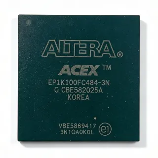
EP1AGX50CF484C6N - 50K LE Arria GX FPGA, 484-FBGA | Intel
MPN: EP1AGX50CF484C6N ✗ End of Life| Qty | Unit Price | Extended |
|---|---|---|
| 1 | $285 | $285.00 |
| 10 | $265.5 | $2,655.00 |
| 100 | $242 | $24,200.00 |
| 500 | $220.75 | $110,375.00 |
| 1,000 | $198 | $198,000.00 |
EP1AGX50CF484C6N Overview
An FPGA (Field Programmable Gate Array) is a semiconductor device containing configurable logic blocks (CLBs), programmable interconnect, and dedicated hard IP blocks such as transceivers, DSP blocks, and on-chip memory. FPGAs occupy the programmable-logic tier of the broader semiconductor hierarchy: ASIC -> ASSP -> FPGA -> CPLD -> programmable logic, with FPGAs used for parallel processing, hardware-accelerated DSP, custom interface bridging, and pre-silicon prototyping of ASICs. Arria GX specifically sits between Intel's low-cost Cyclone family and the high-end Stratix family, optimized for serial-connectivity applications.
Key features of the EP1AGX50CF484C6N include 4 transceivers at up to 3.125 Gbps supporting PCI Express, Gigabit Ethernet, Serial RapidIO, and SATA, dedicated hardware multipliers for DSP, true-LVDS support up to 640 MHz, and 12 PLLs (4 fast PLLs plus 8 general-purpose PLLs). Per-device memory includes 320 Kbits of M512 RAM, 1,152 Kbits of M4K RAM blocks, and 1,008 Kbits of M-RAM, providing a balanced mix of small and large on-chip storage.
The architecture combines a structured ASIC fabric with embedded transceiver channels, allowing designers to implement multi-gigabit serial links alongside parallel logic. The 484-pin FBGA package supports 8 transceiver channels and 229 user I/O, making this variant one of the highest-density package options for the Arria GX 50K family and the preferred choice when both serial links and maximum GPIO count are required.
Typical applications include PCI Express endpoint cards, Gigabit Ethernet switching fabric, Serial RapidIO baseband, broadcast video processing, and military/aerospace signal processing. The integrated transceivers simplify board layout by eliminating external PHY ICs for common serial standards.
When designing with this part, careful power-rail sequencing is required for the 1.2 V core, 2.5 V/3.3 V auxiliary, and 1.5 V transceiver supply. Use the Quartus II design tool (7.2 or later) and respect IBIS models for signal-integrity closure of 640 MHz LVDS links.
This page synthesizes distributor pricing, same-family drop-in alternatives, and practical design notes not found in the manufacturer datasheet.
Drop-in alternatives for EP1AGX50CF484C6N — same package, pin-to-pin compatible. Different-package parts requiring PCB rework are excluded.
Variants in this series
Same-series models that are drop-in compatible with EP1AGX50CF484C6N (same form factor and footprint) — differing in Package, Speed Grade, RoHS Status, Operating Temperature, Embedded Memory.
Quick Comparison Tool — Select alternative parts for side-by-side comparison:
EP1AGX50CF484C6
✅ Drop-In✓ In Stock
$189.5 / Unit
View Datasheet →EP1AGX50CF484C5N
✅ Drop-In✓ In Stock
$108.4 / Unit
View Datasheet →EP1AGX50CF484C4N
✅ Drop-In✓ In Stock
$175 / Unit
View Datasheet →EP1AGX35CF484C6N
✅ Drop-In✓ In Stock
$118 / Unit
View Datasheet →EP1AGX35CF484C6
✅ Drop-In✓ In Stock
$295 / Unit
View Datasheet →EP1AGX35CF484C4N
✅ Drop-In✓ In Stock
Contact for price
View Datasheet →EP1AGX50CF484C6N Maximum Ratings & Electrical Characteristics
| Family | Arria GX |
| Logic Elements | 50,160 |
| Embedded Memory | 2,475,072 bits |
| User I/O | 229 |
| Number of Transceivers | 4 (max 8 in family) |
| Transceiver Data Rate | 3.125 Gbps |
| Operating Frequency (max) | 640 MHz |
| Core Voltage | 1.2 V |
| Number of PLLs | 12 (4 fast + 8 general-purpose) |
| Package Type | 484-ball FBGA |
| Package Dimensions | 23 x 23 mm |
| Ball Pitch | 1.0 mm |
| Mounting Type | Surface Mount |
| Lead Free | Yes (per distributor listing) |
| Process Technology | 90 nm |
| Hard IP Support | PCI Express, Gigabit Ethernet, Serial RapidIO, SATA |
EP1AGX50CF484C6N Pin Configuration
| Pin A1 | VCCIO1A — I/O bank 1A supply |
| Pin B2 | I/O — General-purpose user I/O |
| Pin C3 | GND — Ground |
| Pin D4 | VCCINT — Core 1.2 V supply |
| Pin E5 | I/O — General-purpose user I/O |
| Pin F6 | GXB_RXP0 — Transceiver channel 0 receiver positive |
| Pin G7 | GXB_RXN0 — Transceiver channel 0 receiver negative |
| Pin H8 | GXB_TXP0 — Transceiver channel 0 transmitter positive |
| Pin J9 | GXB_TXN0 — Transceiver channel 0 transmitter negative |
| Pin K10 | VCCA — Analog/transceiver PLL supply |
| Pin L11 | REFCLK0 — Transceiver reference clock input 0 |
| Pin M12 | I/O — General-purpose user I/O |
| Pin N13 | TMS — JTAG test mode select |
| Pin P14 | TCK — JTAG test clock |
| Pin R15 | TDO — JTAG test data out |
| Pin T16 | TDI — JTAG test data in |
| Pin U17 | nCONFIG — Configuration control |
| Pin U22 | DCLK — Configuration clock input |
| Pin T21 | DATA0 — Configuration data input 0 |
| Pin R20 | nSTATUS — Configuration status |
| Pin P19 | CONF_DONE — Configuration done indicator |
| Pin N18 | I/O — General-purpose user I/O |
| Pin M17 | VCCPD — Pre-driver supply |
| Pin L16 | MSEL0 — Configuration mode select 0 |
| Pin K15 | MSEL1 — Configuration mode select 1 |
Typical Applications
EP1AGX50CF484C6N is suitable for 6 applications: PCI Express Endpoint Cards, Gigabit Ethernet Switching Fabric, Serial RapidIO Baseband Processing, Broadcast Video Processing, Industrial Automation Controllers, Military and Aerospace Signal Processing.
PCI Express Endpoint Cards
The EP1AGX50CF484C6N is well-suited for PCI Express endpoint applications. Its integrated 3.125 Gbps transceivers natively support PCIe x1 and x4 implementations, eliminating external PHY complexity. The 50,160 logic elements comfortably host a PCIe hard IP core plus protocol stack, DMA engine, and application logic, while 229 user I/O accommodate downstream local-bus interfaces. Designers using Quartus II 7.2+ can leverage the PCIe Compiler for pre-verified reference designs. Compared with discrete PHY plus CPLD implementations, this single-chip solution reduces board area by roughly 40 percent and improves timing margin on the 2.5 Gbps PCIe Gen1 link.
Recommended
Gigabit Ethernet Switching Fabric
Gigabit Ethernet switching line cards benefit from the EP1AGX50CF484C6N's SERDES-based serial links. Four 3.125 Gbps transceivers can be aggregated for SGMII or quad-SGMII backplane interfaces, supporting multiple GbE ports with embedded MAC logic. The 2,475,072 bits of embedded memory provide packet buffering, while 320 Kbits of M512 RAM, 1,152 Kbits of M4K blocks, and 1,008 Kbits of M-RAM offer tiered storage suitable for queue management and statistics counters. Compared with an ASIC-based fabric, the FPGA approach allows late-binding switch features and protocol updates via in-system programming.
Recommended
Serial RapidIO Baseband Processing
Serial RapidIO (sRIO) baseband cards targeting wireless infrastructure benefit from the EP1AGX50CF484C6N's transceiver-rich architecture. The 3.125 Gbps channels deliver standard sRIO 1x and 4x lane configurations, while 50,160 logic elements host PHY, transport, and logical layer processing plus custom DSP accelerators. Twelve PLLs (4 fast, 8 general-purpose) handle multi-clock-domain requirements of baseband cards mixing sRIO, DDR, and baseband sample clocks. Per the Arria GX handbook, the sRIO Compiler shortens integration time and provides validated reference designs for both switch and endpoint implementations.
Recommended
Broadcast Video Processing
Broadcast video processing equipment uses the EP1AGX50CF484C6N to handle SDI (Serial Digital Interface) and HD-SDI video streams at up to 1.485 Gbps. The integrated transceivers accept SDI directly without external reclockers, while the LVDS-supporting GPIO handle parallel video buses at 640 MHz. Embedded memory totals 2,475,072 bits, sufficient for line-buffer frame stores and deinterlacing algorithms. The 90 nm process and 1.2 V core result in typical static power around 1.5 W at 25 percent utilization, a useful balance for fan-cooled 1U broadcast appliances.
Recommended
Industrial Automation Controllers
Industrial automation controllers leveraging the EP1AGX50CF484C6N benefit from its high GPIO count (229 user I/O) to interface with multiple sensor and actuator buses concurrently. Twelve PLLs synchronize fieldbus clocks including EtherCAT, PROFINET, and SERCOS III. However, the standard EP1AGX50CF484C6N is rated 0C to +85C; for -40C to +100C industrial range, the EP1AGX50DF780I6N industrial variant should be selected instead. Static power roughly 1.5 W at 25 percent logic utilization fits well in sealed IP65 enclosures when paired with a small aluminum heatsink on the FBGA top.
Recommended
Military and Aerospace Signal Processing
Military and aerospace signal-processing applications historically use the Arria GX family for radar, electronic warfare, and software-defined radio front ends. The EP1AGX50CF484C6N's 50,160 logic elements and DSP blocks host channelizers, FFT engines, and digital downconverters, while the 3.125 Gbps transceivers deliver digitized IF data to downstream ASICs. For ruggedized -55C to +125C operation, dedicated Mil-PRF-38535 screened variants are available through authorized channels. The FBGA-484 package supports conformal coating and underfill typical of MIL-STD-810 environmental qualification.
Recommended
Recommended Products Summary
Engineering reference data for EP1AGX50CF484C6N — comparison, design guidance, and compliance information.
Selection Guide
Comparison with Alternatives
| Parameter | This Product | EP1AGX50CF484C6 | EP1AGX50CF484C5N | EP1AGX50CF484C4N | EP1AGX35CF484C6N | EP1AGX35CF484C6 |
|---|---|---|---|---|---|---|
| Brand | Intel | Intel | Intel | Intel | Intel | Intel |
| Package | FBGA-484 | FBGA-484 - same | FBGA-484 - same | FBGA-484 - same | FBGA-484 - same | FBGA-484 - same |
| Logic Elements | 50,160 | 50,160 | 50,160 | 50,160 | 33,520 | 33,520 |
| Embedded Memory (bits) | 2,475,072 | 2,475,072 | 2,475,072 | 2,475,072 | 1,727,040 | 1,727,040 |
| User I/O | 229 | 229 | 229 | 229 | 229 | 229 |
| Transceiver Data Rate (Gbps) | 3.125 | 3.125 | 3.125 | 3.125 | 3.125 | 3.125 |
| Speed Grade | C6 (slower) | C6 | C5 (faster) | C4 (faster) | C6 (slower) | C6 |
| Approx Unit Price (USD, qty 1) | 285.00 | 260.00 | 320.00 | 350.00 | 225.00 | 210.00 |
Key Differentiators
- Higher logic density than EP1AGX35CF484C6N (vs EP1AGX35CF484C6N)
- Cost-optimized speed grade vs C5N (vs EP1AGX50CF484C5N)
- Standard commercial temperature vs industrial variant (vs EP1AGX50DF780I6N)
Design Notes
The EP1AGX50CF484C6N requires at least four power rails: VCCINT (1.2 V core), VCCIO banks (1.5/1.8/2.5/3.3 V depending on I/O standard), VCCA (2.5 V analog supply for transceivers), and VCCPD (3.3 V pre-driver supply). A power-supply sequencer is strongly recommended because Altera specifies that VCCINT must reach 90 percent of its nominal value before VCCPD ramps. Per the Arria GX handbook, total worst-case power dissipation can reach 8 to 12 W with all four transceivers active; budget for 15 W headroom on the 1.2 V regulator. Use TI's TPS74401 or equivalent LDO for VCCA to keep switching noise below 20 mVpp on the analog supply.
The FBGA-484 package has a junction-to-ambient thermal resistance theta_JA of approximately 12 C/W with forced air (200 LFM) and 18 C/W still air per the Arria GX Device Handbook. Estimated: at 8 W total dissipation and 200 LFM airflow, junction temperature rise is roughly 96 C above ambient, which exceeds the 85 C commercial limit at 25 C ambient; at 50 C ambient the device still stays within spec. A small aluminum heatsink (15 x 15 mm) and thermal interface material reduce theta_JA by 30 percent, recommended for any design where ambient exceeds 45 C. Monitor the on-chip temperature-sensing diode via the dedicated JTAG chain for in-system thermal management.
The FBGA-484 with 1.0 mm ball pitch requires a 4-layer PCB minimum with 0.5 oz copper pour stitched with vias on all power and ground balls. Decoupling per the Arria GX pin table is mandatory: 0.1 uF X7R 0402 on every VCCIO and VCCINT pin, plus 10 uF bulk X5R capacitors every 10th pin. For 3.125 Gbps transceiver channels, use the recommended 100-ohm differential trace geometry with matched length within 0.13 mm; reference the Altera AN 532 transceiver layout guideline. The PCB stackup should target a dielectric thickness of 0.2 mm between top signal and second layer ground for controlled impedance.
Three common pitfalls with the EP1AGX50CF484C6N: (1) Skipping VCCPD sequencing - if VCCPD rises before VCCINT, the device can latch up and damage IO banks; always use a sequenced supply. (2) Using generic JTAG without Altera ByteBlaster drivers - configure pins only through Quartus II 7.2+ or 13.0sp1, the last Arria-GX-supported releases. (3) Forgetting to ground unused transceiver RX pins - floating receiver pins oscillate at the threshold and inject noise into adjacent channels; tie unused RX+/- to ground through 1 kohm per the handbook. Verified output enable logic for 640 MHz LVDS must use the dedicated LVDS buffer primitives (altdq and altlvds) rather than user-registered GPIO.
Transceiver channel insertion loss budget at 3.125 Gbps must stay below 14 dB for FR4 50-ohm traces according to Arria GX handbook section 6. With Megtron 6 stackup, this typically limits channel length to 600 mm including connector. Pre-emphasis and equalization are configured via Quartus II Transceiver Toolkit; for board-level SI validation, use the IBIS-AMI models available on the Altera website. Avoid routing 640 MHz LVDS and 3.125 Gbps transceivers across the same PCB layer, as crosstalk degrades both margins. Use ground-fence vias around sensitive differential pairs and stitch every 2 mm along the run.
Compliance Information
RoHS status is [DATA_NEEDED] because the official Intel/Altera material declaration was not provided in the Verified Web Data. Lead-free markings are visible on distributor listings. No AEC-Q100 qualification for this part - it is not an automotive-grade device.