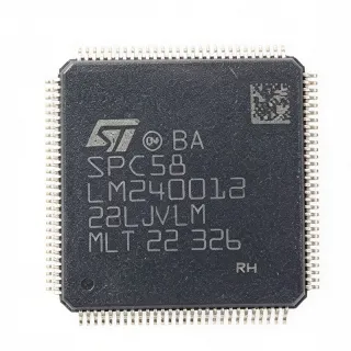
GD32F407ZET6 - 168MHz Cortex-M4 MCU 512KB Flash | GigaDevice
MPN: GD32F407ZET6 ✓ Active| Qty | Unit Price | Extended |
|---|---|---|
| 1 | $4.59 | $4.59 |
| 10 | $4.36 | $43.60 |
| 100 | $4.14 | $414.00 |
| 500 | $3.9 | $1,950.00 |
| 1,000 | $3.49 | $3,490.00 |
GD32F407ZET6 Overview
A microcontroller unit (MCU) is a single-chip computer that integrates a processor core, memory, and programmable peripherals on one die. Within the power-management and embedded-systems hierarchy, an MCU sits above discrete logic and below application processors, executing real-time control and connectivity tasks. The GD32F407 belongs to GigaDevice's GD32F4xx high-performance MCU series, a family positioned as a cost-effective, supply-secure alternative in the mainstream Cortex-M4 segment.
Key features include up to three 12-bit 2.6 MSPS ADCs and two 12-bit DACs for precision analog acquisition, on-chip Ethernet MAC for industrial networking, USB HS/FS OTG for device and host modes, and CAN 2.0B for automotive and industrial fieldbus links. The core achieves Flash zero-wait-state access for maximum execution efficiency, and the peripheral set connects through two APB buses for deterministic I/O timing.
Architecturally, the GD32F407xx integrates the Arm Cortex-M4 processor with its DSP and floating-point instruction extensions, enabling single-cycle MAC and hardware FPU for control-loop mathematics. Peripherals are routed through a multi-layer bus matrix that reduces arbitration contention between the core, DMA controllers, and high-bandwidth interfaces such as Ethernet and USB.
Typical applications include industrial automation controllers, IoT gateways and connectivity nodes, motor drives, and communication equipment, where the combination of 168 MHz throughput, hardware Ethernet, and rich analog peripherals replaces discrete ADC and communication chips.
Design consideration: apply decoupling capacitors at every VDD pin pair, and verify Flash wait-state configuration when operating the core at the full 168 MHz from the internal RC or external crystal clock source.
This page synthesizes distributor pricing, same-family drop-in alternatives, and practical design notes not found in the manufacturer datasheet.
Drop-in alternatives for GD32F407ZET6 — same package, pin-to-pin compatible. Different-package parts requiring PCB rework are excluded.
Variants in this series
Same-series models that are drop-in compatible with GD32F407ZET6 (same form factor and footprint) — differing in Package, SRAM.
Quick Comparison Tool — Select alternative parts for side-by-side comparison:
GD32F407ZGT6
✅ Drop-In ⚠️ Specs Unverified📋 Reference alternative (not in catalog)
GD32F407ZIT6
✅ Drop-In ⚠️ Specs Unverified📋 Reference alternative (not in catalog)
GD32F407ZKT6
✅ Drop-In ⚠️ Specs Unverified📋 Reference alternative (not in catalog)
STM32F407ZET6
✅ Drop-In✓ In Stock
$6.6023 / Unit
View Datasheet →GD32F407ZET6 Maximum Ratings & Electrical Characteristics
| Core Processor | Arm Cortex-M4 32-bit |
| Maximum Clock Frequency | 168 MHz |
| Flash Memory | 512 KB |
| SRAM | 192 KB |
| ADC Resolution | 12 bit |
| ADC Converters | 3 (up to 2.6 MSPS) |
| DAC Resolution | 12 bit |
| DAC Converters | 2 |
| Ethernet | 10/100 MAC on-chip |
| USB | USB HS/FS OTG |
| CAN | CAN 2.0B |
| Bus Architecture | Two APB buses |
| Flash Access | Zero wait states |
| Package | LQFP-144 |
| Mounting Type | Surface Mount |
| Series | GD32F407 |
GD32F407ZET6 lqfp-144 Pin Configuration Guide
Pin configuration for GD32F407ZET6 (lqfp-144 package). This digital IC includes GPIO, communication interfaces (UART, SPI, I2C), and power pins. Refer to the manufacturer datasheet for alternate pin functions and configuration options. Essential for embedded system design and PCB layout.
No detailed pinout data available for GD32F407ZET6.
Refer to the datasheet for full pin configuration.
Typical Applications
GD32F407ZET6 is suitable for 6 applications: Industrial Automation Controllers, IoT Gateways and Connectivity Nodes, Motor Drives and Power Control, Test and Measurement Instruments, Communication and Networking Equipment, Medical and Portable Monitoring Devices.
Industrial Automation Controllers
The GD32F407ZET6 fits programmable logic controllers, remote I/O modules, and motion controllers because its 168 MHz Cortex-M4 core with hardware FPU executes PID and field-oriented-control loops deterministically while the three 12-bit 2.6 MSPS ADCs sample multiple current and voltage channels concurrently. On-chip CAN 2.0B connects to CANopen or DeviceNet fieldbuses, and the Ethernet MAC links the node to factory SCADA networks without an external MAC chip. Used as the main controller with peripherals on two APB buses, it delivers STM32F407-class throughput at lower cost; the main trade-off is re-validating Flash wait-state timing at full clock speed during firmware porting from other cores.
Recommended
IoT Gateways and Connectivity Nodes
For IoT edge gateways, the GD32F407ZET6 combines a 10/100 Ethernet MAC, USB HS/FS OTG, and CAN 2.0B in one 512 KB Flash device, letting a single MCU bridge sensor buses (CAN, RS-485 via USART) to IP networks. The 192 KB SRAM provides adequate buffer space for TCP/IP stacks plus multiple protocol frames, and the 168 MHz core with DSP instructions runs TLS and packet processing with headroom. Deployed between field devices and a cloud uplink, it reduces BOM count versus MCU-plus-external-MAC solutions; designers should budget DMA bandwidth carefully when Ethernet, USB, and multi-channel ADC sampling run concurrently to avoid bus-matrix contention.
Recommended
Motor Drives and Power Control
In variable-frequency drives and servo drives, the GD32F407ZET6's three 12-bit ADCs at 2.6 MSPS enable simultaneous phase-current sampling synchronized to PWM timer triggers, while the Cortex-M4 FPU computes Clarke/Park transforms at 168 MHz for field-oriented control. Twelve-bit DAC channels provide reference or monitoring outputs, and multiple advanced timers generate complementary PWM with dead-band insertion for inverter bridges. Using this MCU as the control core eliminates a separate ADC or DSP in mid-range drives, cutting cost; the critical design consideration is ADC front-end filtering and careful grounding of the analog supply to preserve the 12-bit effective resolution in noisy inverter environments.
Recommended
Test and Measurement Instruments
Bench instruments, data loggers, and hand-held meters benefit from the GD32F407ZET6's analog subsystem: up to three 12-bit 2.6 MSPS ADCs capture multi-channel signals, and the two 12-bit DACs generate stimulus or calibration references. The zero-wait-state Flash access keeps measurement loops jitter-free at 168 MHz, while USB OTG provides direct PC connectivity for data upload and instrument control, and an external Ethernet PHY adds LXI-style networked operation. In this role the MCU handles acquisition, processing, and communication in one chip; designers should allocate the ADC sampling window and DMA buffers carefully to sustain full 2.6 MSPS throughput across all active channels during continuous acquisition.
Recommended
Communication and Networking Equipment
Industrial switches, protocol converters, and modular communication controllers use the GD32F407ZET6's on-chip Ethernet MAC with hardware DMA to move frames at line rate with minimal CPU load, while its CAN 2.0B and multiple USARTs translate between fieldbus and IP protocols. The 168 MHz Cortex-M4 with DSP extensions processes CRC, checksums, and light protocol stacks efficiently, and 192 KB SRAM sustains multiple packet buffers plus descriptor rings. Deployed as a protocol-bridging processor, it replaces MCU-plus-MAC two-chip designs and reduces BOM cost; the key performance consideration is sizing the DMA descriptor and buffer memory so burst traffic does not overflow SRAM under worst-case load.
Recommended
Medical and Portable Monitoring Devices
Patient monitors, portable analyzers, and diagnostic instruments leverage the GD32F407ZET6's low-noise 12-bit ADC channels for biopotential and sensor signal acquisition, with the FPU-accelerated 168 MHz core running digital filtering and basic DSP algorithms locally. USB OTG enables direct data transfer to PCs or charging/accessory peripherals, and an optional Ethernet interface supports networked clinical installations. As the central processing and acquisition engine, the device consolidates functions that otherwise require an MCU plus external data converter; the design consideration is analog front-end layout—guard the ADC inputs and reference, and use separate analog supply decoupling—to reach the full 12-bit effective number of bits on microvolt-level biosignals.
Recommended
Recommended Products Summary
Engineering reference data for GD32F407ZET6 — comparison, design guidance, and compliance information.
Selection Guide
Comparison with Alternatives
| Parameter | This Product | GD32F407ZGT6 | GD32F407ZIT6 | GD32F407ZKT6 | STM32F407ZET6 |
|---|---|---|---|---|---|
| Package | LQFP-144 | LQFP-144 - same | LQFP-144 - same | LQFP-144 - same | LQFP-144 - same |
| Brand | GigaDevice | GigaDevice | GigaDevice | GigaDevice | STMicroelectronics |
| Core / Max Frequency | Arm Cortex-M4, 168 MHz | Arm Cortex-M4, 168 MHz | Arm Cortex-M4, 168 MHz | Arm Cortex-M4, 168 MHz | Arm Cortex-M4, 168 MHz |
| Flash Memory | 512 KB | 1024 KB | 2048 KB | 3072 KB | 512 KB |
| SRAM | 192 KB | 192 KB | 192 KB | 192 KB | 192 KB (+64 KB CCM) |
| ADC | 3 x 12-bit, 2.6 MSPS | 3 x 12-bit, 2.6 MSPS | 3 x 12-bit, 2.6 MSPS | 3 x 12-bit, 2.6 MSPS | 3 x 12-bit, 2.4 MSPS |
| Ethernet / USB / CAN | Yes / HS-FS OTG / CAN 2.0B | Yes / HS-FS OTG / CAN 2.0B | Yes / HS-FS OTG / CAN 2.0B | Yes / HS-FS OTG / CAN 2.0B | Yes / HS-FS OTG / CAN 2.0B |
Key Differentiators
- Flash headroom without footprint change (vs GD32F407ZKT6)
- Cost-down vs the original reference part (vs STM32F407ZET6)
- Supply-chain second source (vs STM32F407ZET6)
Design Notes
Provide independent 3.3V decoupling (100 nF ceramic plus bulk) at every VDD/VDDA pin pair of the LQFP-144, placed within 2 mm of each pin. Separate the analog 3.3V rail through an RC or ferrite filter for VDDA to preserve the 12-bit ADC performance, since the three 2.6 MSPS converters are sensitive to digital supply noise. Estimated: with a typical core-plus-peripheral current in the tens-of-mA range, a linear pre-regulator dissipating (5V-3.3V) x 50 mA is about 85 mW, acceptable without heatsinking.
The LQFP-144 exposes no thermal pad, but the peripheral ring layout still benefits from a solid ground plane on layer 2. Route the Ethernet RMII/RGMII traces as length-matched groups with 50-ohm impedance to the external PHY, and keep the 25 MHz PHY crystal loop small. Place the 0.1 uF VDDA filter capacitor and any VREF decoupling directly at the pins. For USB HS routing, use controlled-impedance 90-ohm differential pairs; for FS, normal GPIO-class routing is acceptable.
When porting from STM32F407 firmware, do not assume identical Flash wait-state and clock-tree register timing - the GD32F407 reaches 168 MHz with zero-wait-state Flash access per its datasheet, but the configuration sequence differs and industry guidance (JLink STM32-to-GD32 guide) recommends re-validating firmware timing before production. Also verify pin alternate-function mappings against the GD32 datasheet pin definition table, since multiplexing differs from the ST original on some pins.
Compliance Information
Compliance status not stated in the provided verified web data; consult GigaDevice product page and official RoHS/REACH declarations.