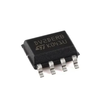
HMC649A - 6-Bit Digital Phase Shifter 3-6 GHz | Analog Devices
MPN: HMC649A ✓ Active| Qty | Unit Price | Extended |
|---|---|---|
| 1 | $0 | $0.00 |
| 10 | $0 | $0.00 |
| 100 | $0 | $0.00 |
| 500 | $0 | $0.00 |
| 1,000 | $0 | $0.00 |
HMC649A Overview
A digital phase shifter is a critical component in RF and microwave systems that alters the phase of an incoming signal by a discrete amount, controlled by digital bits. It is used in phased array antennas, radar systems, and communication systems to steer beams electronically. The HMC649A belongs to the category of RF phase shifters, which are essential for beamforming and signal conditioning in modern wireless infrastructure.
Key features of the HMC649A include 6-bit resolution providing 64 phase states, a frequency range of 3 GHz to 6 GHz, and a typical insertion loss of dB. The device operates with a supply voltage of Vdd=+5V and Vss=-5V, and control voltage of 0/+5V. It is recommended for new designs and is available in a 28-QFN (6x6 mm) package, suitable for surface mount assembly.
The HMC649A utilizes GaAs MMIC technology, offering high performance and reliability for demanding RF applications. The device's low RMS phase error and consistent insertion loss across all states ensure accurate beamforming and signal integrity. Its compact package and 50 Ohm internal matching simplify PCB design and reduce external component count.
Typical applications include phased array radar, satellite communications, and 5G beamforming systems. The HMC649A is also used in test and measurement equipment for phase calibration and in electronic warfare systems for signal manipulation.
When designing with the HMC649A, ensure proper power supply decoupling and control logic interfacing. The device requires both positive and negative supply rails, and the control lines should be driven with appropriate logic levels to achieve accurate phase states.
Drop-in alternatives for HMC649A — same package, pin-to-pin compatible. Different-package parts requiring PCB rework are excluded.
Variants in this series
Same-series models that are drop-in compatible with HMC649A (same form factor and footprint) — differing in Frequency Range, Package, Control Logic, Impedance, Insertion Loss Variation.
Quick Comparison Tool — Select alternative parts for side-by-side comparison:
HMC649ALP6E
✅ Drop-In✓ In Stock
$29 / Unit
View Datasheet →HMC649
✅ Drop-In📋 Reference alternative (not in catalog)
MAPS-010164
✅ Drop-In ⚠️ Specs Unverified📋 Reference alternative (not in catalog)
MAPS-010165
✅ Drop-In ⚠️ Specs Unverified📋 Reference alternative (not in catalog)
ADAR1000
✅ Drop-In ⚠️ Specs Unverified✓ In Stock
$130 / Unit
View Datasheet →HMC649A Specifications (manufacturer-published)
| Frequency Range | 3 GHz to 6 GHz |
| Phase Resolution | 6-bit (64 states) |
| RMS Phase Error | 4 degrees (typical) |
| Insertion Loss Variation | ±0.5 dB across all phase states |
| Control Logic | Positive, 0/+5V |
| Supply Voltage (Vdd) | +5V |
| Supply Voltage (Vss) | -5V |
| Impedance | 50 Ohm (internally matched) |
| Package | 28-QFN (6x6 mm) |
| Mounting Type | Surface Mount |
| Technology | GaAs MMIC |
| RoHS Status | Compliant |
HMC649A Pin Configuration
| Pin 1 | VDD — Positive supply voltage (+5V) |
| Pin 2 | GND — Ground |
| Pin 3 | RFIN — RF input |
| Pin 4 | GND — Ground |
| Pin 5 | RFOUT — RF output |
| Pin 6 | GND — Ground |
| Pin 7 | VSS — Negative supply voltage (-5V) |
| Pin 8 | CTL1 — Control bit 1 (LSB) |
| Pin 9 | CTL2 — Control bit 2 |
| Pin 10 | CTL3 — Control bit 3 |
| Pin 11 | CTL4 — Control bit 4 |
| Pin 12 | CTL5 — Control bit 5 |
| Pin 13 | CTL6 — Control bit 6 (MSB) |
| Pin 14 | GND — Ground |
Power & Thermal Characteristics
| Power Input | +5V |
Power input and thermal parameters for HMC649A as published by the manufacturer.
Typical Applications
HMC649A is suitable for 6 applications: Phased Array Radar, Satellite Communication, 5G Beamforming, Test and Measurement, Electronic Warfare, Point-to-Point Communication.
Phased Array Radar
The HMC649A's 6-bit phase resolution and low RMS phase error of 4 degrees enable precise beam steering in phased array radar systems. Its ±0.5 dB insertion loss variation ensures uniform amplitude across all phase states, maintaining sidelobe levels and detection accuracy. The device operates from 3 to 6 GHz, covering C-band radar frequencies, and its 50 Ohm internal matching simplifies integration into antenna arrays.
Recommended
Satellite Communication
In satellite communication systems, the HMC649A provides precise phase control for beamforming and signal conditioning. Its frequency range of 3-6 GHz covers C-band uplink and downlink frequencies. The low insertion loss variation of ±0.5 dB ensures consistent signal strength across all phase states, which is critical for maintaining link budget. The compact 28-QFN package is ideal for space-constrained satellite payloads.
Recommended
5G Beamforming
The HMC649A is well-suited for 5G beamforming applications, operating in the 3-6 GHz band used for 5G NR. Its 6-bit phase resolution allows fine beam steering, and the low RMS phase error of 4 degrees ensures accurate beam direction. The device's positive control logic (0/+5V) simplifies interface with baseband processors. Its 50 Ohm internal matching reduces external component count, enabling compact antenna modules.
Recommended
Test and Measurement
In test and measurement equipment, the HMC649A is used for phase calibration and signal conditioning. Its precise phase steps and low insertion loss variation make it ideal for calibrating phase shifters and verifying system performance. The device's wide frequency range (3-6 GHz) covers many test applications, and its compact package allows integration into portable test instruments.
Recommended
Electronic Warfare
The HMC649A is used in electronic warfare systems for signal manipulation and beam steering. Its fast phase switching and high accuracy (RMS phase error of 4 degrees) enable rapid response to threats. The device's 3-6 GHz frequency range covers many radar and communication bands, and its rugged GaAs MMIC construction ensures reliability in harsh environments.
Recommended
Point-to-Point Communication
In point-to-point microwave links, the HMC649A provides phase adjustment for antenna alignment and polarization control. Its 6-bit resolution allows fine phase tuning, and the low insertion loss variation ensures minimal signal degradation. The device's 50 Ohm internal matching simplifies integration into transceiver chains, and its compact package is suitable for outdoor units.
Recommended
Recommended Products Summary
Engineering reference data for HMC649A — comparison, design guidance, and compliance information.
Selection Guide
Comparison with Alternatives
| Parameter | This Product | HMC649ALP6E | HMC649 | MAPS-010164 |
|---|---|---|---|---|
| Package | 28-QFN (6x6 mm) | 28-QFN (6x6 mm) | 28-QFN (6x6 mm) | 28-QFN (6x6 mm) |
| Brand | Analog Devices | Analog Devices | Analog Devices | MACOM |
| Frequency Range | 3 GHz to 6 GHz | 3 GHz to 6 GHz | 3 GHz to 6 GHz | 2-6 GHz |
| Phase Resolution | 6-bit (64 states) | 6-bit (64 states) | 6-bit (64 states) | 6-bit (64 states) |
| RMS Phase Error | 4 degrees | 4 degrees | 4 degrees | 5 degrees |
| Insertion Loss Variation | ±0.5 dB | ±0.5 dB | ±0.5 dB | ±1 dB |
| Supply Voltage | +5V / -5V | +5V / -5V | +5V / -5V | +5V / -5V |
| Control Logic | 0/+5V | 0/+5V | 0/+5V | 0/+5V |
Key Differentiators
- Low RMS phase error of 4 degrees (vs MAPS-010164)
- Extremely low insertion loss variation of ±0.5 dB (vs MAPS-010164)
- Recommended for new designs (vs HMC649)
Design Notes
The HMC649A requires dual supply voltages: Vdd=+5V and Vss=-5V. Ensure proper decoupling on both supply pins with 100nF capacitors placed close to the device. The control logic operates at 0/+5V, so level shifting may be needed if interfacing with 3.3V logic.
The HMC649A is internally matched to 50 Ohms, so no external matching components are required. However, maintain 50 Ohm transmission line impedance on the RF input and output traces. Use ground vias around the exposed pad to ensure good thermal and electrical grounding.
Ensure the control bits are set correctly to achieve the desired phase state. Incorrect logic levels can result in phase errors. Also, verify that the supply voltages are within the specified range to avoid damage. Refer to the datasheet for the truth table and absolute maximum ratings.
Compliance Information
RoHS compliance is indicated by Analog Devices. Other compliance data not specified in the provided data.