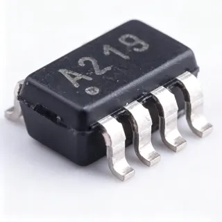
INA219AIDCNR - 26V 12-bit I2C Power Monitor | Texas Instruments
MPN: INA219AIDCNR ✓ Active| Qty | Unit Price | Extended |
|---|---|---|
| 1 | $2.1 | $2.10 |
| 10 | $1.89 | $18.90 |
| 100 | $1.62 | $162.00 |
| 500 | $1.38 | $690.00 |
| 1,000 | $1.15 | $1,150.00 |
INA219AIDCNR Overview
A current shunt monitor is an integrated circuit that measures the voltage across a sense resistor in series with a load, converting a small differential signal into a precise current reading. Within the power management IC hierarchy, current sense amplifiers such as the INA219 sit alongside voltage regulators and battery management ICs, providing the telemetry needed for system monitoring, protection, and efficiency optimization. The bidirectional architecture supports measurement of current flowing in both directions, essential for battery charge/discharge monitoring.
Key features include a 12-bit ADC with programmable gain (0.125, 0.25, 0.5, and 1 V/V), a common-mode range of 0 to 26 V, 16 selectable I2C addresses via the A0/A1 pins, and a programmable calibration register combined with an internal multiplier enabling direct readouts of current in amperes and power in watts. The A grade provides an input offset of plus or minus 50 uV (max) and offset drift of plus or minus 0.5 uV/C (max).
Technically, the zero-drift chopper-stabilized architecture maintains accuracy over the full -40C to +125C operating range. Programmable conversion time and averaging let engineers trade conversion speed against measurement noise. The SOT-23-8 package measures approximately 2.9 mm x 1.6 mm, suiting space-constrained designs.
Typical applications include battery chargers, server power monitoring, telecom equipment, and power supplies, where accurate current and power telemetry is critical. It is also used in industrial load monitoring and fault detection.
Design tip: place the shunt in the high-side path, decouple VS with a 0.1 uF capacitor close to the pin, and configure A0/A1 to avoid I2C address conflicts on the bus. Pricing as of 2026-08-30 from authorized distributors.
Drop-in alternatives for INA219AIDCNR — same package, pin-to-pin compatible. Different-package parts requiring PCB rework are excluded.
Variants in this series
Same-series models that are drop-in compatible with INA219AIDCNR (same form factor and footprint) — differing in ADC Resolution, Interface, MSL Level, Operating Temperature, Package.
Quick Comparison Tool — Select alternative parts for side-by-side comparison:
INA219BIDCNR
✅ Drop-In📋 Reference alternative (not in catalog)
INA219AIDCNR
✅ Drop-In✓ In Stock
$1.49 / Unit
View Datasheet →INA219AIDCNT
✅ Drop-In📋 Reference alternative (not in catalog)
INA219AIDCNR Specifications
| Function | High-side current shunt and power monitor |
| Interface | I2C / SMBus compatible |
| ADC Resolution | 12 bit |
| Bus Voltage Range (Common-Mode) | 0 V to 26 V |
| Supply Voltage Range | 3 V to 5.5 V |
| Supply Current (Max) | 1 mA |
| Input Offset (A Grade, Max) | ±50 uV |
| Input Offset Drift (Max) | ±0.5 uV/C |
| Programmable Gain | 0.125, 0.25, 0.5, 1 V/V |
| I2C Addresses | 16 programmable (A0/A1 pins) |
| Calibration | Programmable calibration register with internal multiplier |
| Operating Temperature | -40C to +125C |
| Package | SOT-23-8 (DCN) |
| Mounting Type | Surface Mount |
| Measurement Type | Bidirectional (charge/discharge) |
| RoHS Status | Compliant |
| MSL Level | 2 (260C, 1 year) |
INA219AIDCNR Pin Configuration
| Pin 1 | IN+ — Shunt positive sense input (connect to bus side of shunt) |
| Pin 2 | IN- — Shunt negative sense input (connect to load side of shunt) |
| Pin 3 | GND — Ground reference |
| Pin 4 | VS — Power supply, 3 V to 5.5 V |
| Pin 5 | SDA — I2C/SMBus data (also usable as address strap A1) |
| Pin 6 | SCL — I2C/SMBus clock (also usable as address strap A0) |
| Pin 7 | A0 — I2C address select 0 |
| Pin 8 | A1 — I2C address select 1 |
Typical Applications
INA219AIDCNR is suitable for 6 applications: Battery Chargers, Server and Datacenter Power Monitoring, Telecom Equipment Power Supervision, Industrial Load Monitoring and Fault Detection, Power Supply Telemetry, Automotive Battery and Load Monitoring.
Battery Chargers
The INA219AIDCNR fits battery charging systems because its bidirectional sensing measures both charge and discharge current through a single high-side shunt, with the 0 to 26 V common-mode range covering 1S-5S battery stacks and 5 V/12 V charge rails. Placed between the charger output and the battery pack with a 10-100 mOhm shunt, the 12-bit ADC and programmable calibration register report current in amperes and power in watts directly over I2C, enabling coulomb-style state-of-charge estimation by a host MCU.
Recommended
Server and Datacenter Power Monitoring
In server boards, the INA219AIDCNR provides per-rail current and power telemetry that datacenter BMCs use for power capping and efficiency optimization. Its 1 mA maximum supply current and 0 to 26 V common-mode range suit 12 V intermediate bus monitoring, while 16 selectable I2C addresses (via A0/A1) allow many monitors on one SMBus. The SOT-23-8 footprint (about 2.9 mm x 1.6 mm) fits dense voltage-regulator layouts, and programmable averaging reduces noise for stable power readings.
Recommended
Telecom Equipment Power Supervision
Telecom shelves use the INA219AIDCNR to supervise -48 V-derived and 12 V/24 V distribution rails. The device senses across high-side shunts on buses up to 26 V with ±50 uV maximum input offset (A grade) and zero-drift architecture holding ±0.5 uV/C drift from -40C to +125C, delivering accurate current data for fault detection and load balancing. The I2C/SMBus-compatible interface integrates directly with shelf-management microcontrollers, and conversion-time programmability lets designers trade speed against measurement noise.
Recommended
Industrial Load Monitoring and Fault Detection
Industrial automation nodes employ the INA219AIDCNR to detect stalled motors, open loads, and overcurrent conditions by continuously reading bus current and power over I2C. The wide -40C to +125C operating range and zero-drift chopper architecture maintain accuracy in electrically noisy factory environments, while the 0 to 26 V common-mode range covers standard 24 V industrial rails. Its 16-address I2C scheme lets a single PLC-side controller poll dozens of channels, and filtering options suppress PWM-induced ripple on switched loads.
Recommended
Power Supply Telemetry
AC-DC and DC-DC power supplies integrate the INA219AIDCNR on output rails to report real-time current and power for digital-power interfaces. The internal multiplier combined with the programmable calibration register yields direct watt readouts without host-side math, and the 12-bit ADC with programmable conversion times supports both fast transient event capture and low-noise averaged logging. With only 1 mA quiescent consumption and a SOT-23-8 footprint, the monitor adds negligible overhead to standby power budgets.
Recommended
Automotive Battery and Load Monitoring
For automotive designs, the AEC-Q100-qualified INA219AIDCNR-Q1 drop-in variant enables high-side monitoring of 12 V battery buses and switched loads. The bidirectional measurement distinguishes charging from cranking/discharge current, and the zero-drift offset drift of ±0.5 uV/C keeps accuracy across the full -40C to +125C automotive ambient range. I2C telemetry integrates with body-control MCUs for load-shedding decisions and battery-state estimation, and up to 16 addresses support multi-zone monitoring architectures.
Recommended
Recommended Products Summary
Engineering reference data for INA219AIDCNR — comparison, design guidance, and compliance information.
Selection Guide
Comparison with Alternatives
| Parameter | This Product | INA219BIDCNR | INA219AIDCNR-Q1 | INA219AIDCNT |
|---|---|---|---|---|
| Package | SOT-23-8 (DCN) | SOT-23-8 (DCN) - same | SOT-23-8 (DCN) - same | SOT-23-8 (DCN) - same |
| Brand | Texas Instruments | Texas Instruments | Texas Instruments | Maxim Integrated |
| ADC Resolution | 12 bit | 12 bit | 12 bit | 16 bit |
| Bus Common-Mode Range | 0 V to 26 V | 0 V to 26 V | 0 V to 26 V | 0 V to 36 V |
| Interface | I2C / SMBus | I2C / SMBus | I2C / SMBus | Analog output (no digital interface) |
| Automotive Grade | No | No | Yes (AEC-Q100) | Yes (AEC-Q100) |
| Operating Temperature | -40C to +125C | -40C to +125C | -40C to +125C | -40C to +125C |
Key Differentiators
- Cost-optimized A grade for high-volume designs (vs INA219BIDCNR)
- Automotive drop-in available (vs INA219AIDCNR-Q1)
- Integrated digital interface vs analog amps (vs AD8418)
Design Notes
Place the shunt resistor in the high-side path with Kelvin connections: route IN+ and IN- directly to the shunt pads with short, symmetric traces to avoid measuring PCB IR drop. Decouple VS with a 0.1 uF ceramic capacitor placed within 2 mm of pin 4. Keep the I2C traces short and add 4.7 kOhm pull-ups to the correct bus voltage. Per TI application guidance, the shunt ground reference must tie to the device GND pin at a single point to prevent ground-loop offset errors.
Strap A0 and A1 intentionally - floating or conflicting address straps are the most common bring-up failure. With A0/A1 tied to GND, VS, SDA, or SCL you get 16 addresses, but tying to SDA/SCL creates dynamic addresses that some I2C masters mis-handle. Also remember the programmable gain sets full-scale shunt drop (40/80/160/320 mV): sizing gain and shunt together determines resolution - a 10 mOhm shunt at gain 8 (320 mV FS) supports up to 32 A but reduces resolution for low loads.
On PWM-switched or noisy rails, use the programmable conversion time and averaging registers to filter ripple - longer averaging windows (e.g., 12-bit conversion with 128x averaging) trade response latency for stable power telemetry. Do not extend IN+ / IN- traces near switching nodes of buck converters; route them on a quiet layer. According to TI datasheet SBOS448, filtering options in the device configuration register further suppress wideband noise before the ADC input.
Compliance Information
RoHS compliant and MSL 2 (260C, 1 year) per distributor data (PartGenie). AEC-Q100 not applicable to standard grade; the INA219AIDCNR-Q1 variant is qualified for automotive. REACH status not stated in provided data.