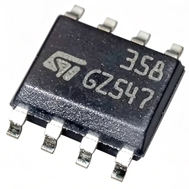
LM358DT - Dual Low Power Op Amp | STMicroelectronics | SOIC-8
MPN: LM358DT ✓ Active| Qty | Unit Price | Extended |
|---|---|---|
| 1 | $0.0873 | $0.09 |
| 10 | $0.063 | $0.63 |
| 100 | $0.0558 | $5.58 |
| 500 | $0.0533 | $26.65 |
| 1,000 | $0.0509 | $50.90 |
LM358DT Overview
An operational amplifier (op-amp) is a high-gain voltage amplifier with differential inputs and a single-ended output. It is a fundamental building block in analog electronics, used for signal conditioning, filtering, and mathematical operations. The LM358 is part of the general-purpose op-amp family, which includes the LM324 (quad version) and LM393 (comparator). These devices are widely used in industrial, automotive, and consumer electronics due to their low cost, ease of use, and wide supply voltage range.
Key features of the LM358DT include a wide supply voltage range (3V to 32V), low quiescent current (350 µA per amplifier), and a common-mode input voltage range that includes ground, allowing single-supply operation. The output stage can sink and source current, and the device is short-circuit protected. The LM358DT also features a typical input offset voltage of 2 mV and a gain-bandwidth product of 1.1 MHz, making it suitable for low-frequency signal processing.
The LM358DT uses a bipolar transistor architecture with a class-AB output stage, providing low crossover distortion. The input stage is a PNP differential pair, which allows the input common-mode range to extend to the negative supply rail (ground in single-supply operation). This design enables direct sensing of signals near ground, a key advantage in battery-powered and single-supply systems.
Typical applications include transducer amplifiers, DC gain blocks, active filters, and signal conditioning in industrial control systems. The LM358DT is also used in portable instrumentation, power supply monitoring, and automotive sensor interfaces. Its low power consumption makes it ideal for battery-operated devices.
When designing with the LM358DT, ensure that the input common-mode voltage does not exceed the specified range, and provide adequate decoupling capacitors on the power supply pins. The output can drive loads down to 2 kΩ, but for heavier loads, consider using a buffer stage. The device is stable with capacitive loads up to 500 pF, but for larger loads, an external compensation network may be required.
This page synthesizes distributor pricing, drop-in alternatives, and practical design notes not found in the STMicroelectronics datasheet, providing engineers with a comprehensive resource for selecting and using the LM358DT.
Drop-in alternatives for LM358DT — same package, pin-to-pin compatible. Different-package parts requiring PCB rework are excluded.
Variants in this series
Same-series models that are drop-in compatible with LM358DT (same form factor and footprint) — differing in Input Bias Current, Package.
Quick Comparison Tool — Select alternative parts for side-by-side comparison:
LM358DR
✓ In Stock
$0.0514 / Unit
View Datasheet →LM2904DR
✓ In Stock
$0.1 / Unit
View Datasheet →LM358ADT
📋 Reference alternative (not in catalog)
LM358DT Maximum Ratings & Electrical Characteristics
| Number of Channels | 2 |
| Supply Voltage (Single) | 3 V to 32 V |
| Supply Voltage (Split) | ±1.5 V to ±16 V |
| Quiescent Current (per Amp) | 350 µA (typical) |
| Input Offset Voltage | 2 mV (typical) |
| Input Bias Current | 45 nA (typical) |
| Gain-Bandwidth Product | 1.1 MHz |
| Slew Rate | 0.6 V/µs |
| Common-Mode Rejection Ratio | 85 dB (typical) |
| Power Supply Rejection Ratio | 100 dB (typical) |
| Output Current | 40 mA (source/sink) |
| Operating Temperature Range | 0°C to +70°C |
| Package | SOIC-8 (SO-8) |
| Mounting Type | Surface Mount |
| RoHS Status | Compliant |
LM358DT Pin Configuration
| Pin 1 | OUT1 — Output of amplifier 1 |
| Pin 2 | IN1- — Inverting input of amplifier 1 |
| Pin 3 | IN1+ — Non-inverting input of amplifier 1 |
| Pin 4 | VCC- — Negative supply (ground in single-supply) |
| Pin 5 | IN2+ — Non-inverting input of amplifier 2 |
| Pin 6 | IN2- — Inverting input of amplifier 2 |
| Pin 7 | OUT2 — Output of amplifier 2 |
| Pin 8 | VCC+ — Positive supply |
Typical Applications
LM358DT is suitable for 6 applications: Transducer Amplifier, DC Gain Block, Active Filter, Signal Conditioning, Portable Instrumentation, Power Supply Monitoring.
Transducer Amplifier
The LM358DT is ideal for amplifying signals from sensors such as thermocouples, strain gauges, and photodiodes. Its low quiescent current (350 µA) and wide supply range (3V to 32V) allow it to be powered directly from a battery or a 24V industrial supply. In a typical configuration, the op-amp is used in a non-inverting or differential amplifier topology to condition the small sensor output to a level suitable for an ADC. The input common-mode range includes ground, enabling direct connection to sensors that output near-zero voltages. The gain-bandwidth product of 1.1 MHz is sufficient for DC and low-frequency signals, and the low input bias current (45 nA) minimizes errors when driving high-impedance sensors. For best accuracy, use precision resistors in the feedback network and bypass the power supply with a 0.1 µF capacitor.
Recommended
DC Gain Block
The LM358DT can be used as a DC gain block to amplify small DC voltages from sensors or potentiometers. Its low offset voltage (2 mV typical) and high DC gain (100 dB) make it suitable for precision measurement. In a non-inverting configuration, the gain is set by two resistors, and the output can drive loads up to 40 mA. The wide supply voltage range allows the op-amp to operate from a single 5V rail or a 24V industrial supply. The device's low power consumption is beneficial in multi-channel systems where many op-amps are used. To minimize offset errors, use a trim potentiometer in the offset nulling circuit if available. The LM358DT's output can swing close to the positive rail, but not to the negative rail, so consider this when designing the output range.
Recommended
Active Filter
The LM358DT can be used to implement active filters such as low-pass, high-pass, and band-pass filters for signal conditioning. Its gain-bandwidth product of 1.1 MHz limits the filter cutoff frequency to a few hundred kHz, which is adequate for audio and sensor signals. In a Sallen-Key topology, the op-amp provides gain and buffering, allowing the filter to drive subsequent stages without loading. The low quiescent current is advantageous in battery-powered filters. When designing the filter, choose component values that keep the op-amp within its linear output range, and ensure the input common-mode voltage is within the specified range. The LM358DT's output can drive capacitive loads up to 500 pF, but for larger loads, add a series resistor to isolate the output.
Recommended
Signal Conditioning
The LM358DT is widely used for signal conditioning in industrial and automotive applications, such as converting current signals from sensors to voltage levels. Its wide supply range and low power consumption make it suitable for 4-20 mA current loop receivers, where the op-amp converts the loop current to a voltage using a precision resistor. The input common-mode range includes ground, allowing direct connection to the sense resistor. The device's low input bias current minimizes errors in high-impedance circuits. In a typical application, the LM358DT is configured as a difference amplifier to reject common-mode noise. The output can be fed directly to an ADC or a microcontroller. For best performance, use a precision resistor network and bypass the power supply with a 10 µF electrolytic capacitor in parallel with a 0.1 µF ceramic capacitor.
Recommended
Portable Instrumentation
The LM358DT is ideal for portable instrumentation due to its low quiescent current (350 µA) and wide supply voltage range (3V to 32V). It can be powered directly from a 9V battery or a 3.3V supply, making it versatile for handheld devices. In a typical application, the op-amp is used to amplify signals from a thermocouple or a pH sensor, and the output is read by a microcontroller's ADC. The low input bias current (45 nA) is beneficial for high-impedance sensors. The device's small SOIC-8 package saves board space, which is critical in portable designs. To extend battery life, consider using the op-amp in a low-power mode by reducing the supply voltage to the minimum required. The LM358DT's output can drive small loads directly, but for driving a display or a buzzer, use a transistor buffer.
Recommended
Power Supply Monitoring
The LM358DT can be used to monitor power supply voltages and generate alarms or control signals. Its wide supply range allows it to operate from the same rail it is monitoring, and its low quiescent current is beneficial in always-on monitoring circuits. In a typical application, the op-amp is configured as a comparator with hysteresis to detect undervoltage or overvoltage conditions. The output can drive an LED or a relay through a transistor. The input common-mode range includes ground, enabling direct connection to the sense resistor. The device's high PSRR (100 dB) ensures accurate monitoring even with noisy supplies. For reliable operation, add a small capacitor to the feedback network to filter noise, and ensure the input voltage does not exceed the supply rails.
Recommended
Recommended Products Summary
Engineering reference data for LM358DT — comparison, design guidance, and compliance information.
Selection Guide
Comparison with Alternatives
| Parameter | This Product | LM358DR | LM2904DR | LM358ADT |
|---|---|---|---|---|
| Package | SOIC-8 | SOIC-8 | SOIC-8 | SOIC-8 |
| Supply Voltage Range | 3V to 32V | 3V to 32V | 3V to 32V | 3V to 32V |
| Quiescent Current (per Amp) | 350 µA | 350 µA | 350 µA | 350 µA |
| Input Offset Voltage (typical) | 2 mV | 2 mV | 2 mV | 1 mV |
| Gain-Bandwidth Product | 1.1 MHz | 1.1 MHz | 1.1 MHz | 1.1 MHz |
| Operating Temperature Range | 0°C to +70°C | 0°C to +70°C | -40°C to +125°C | 0°C to +70°C |
| Output Current | 40 mA | 40 mA | 40 mA | 40 mA |
| RoHS Status | Compliant | Compliant | Compliant | Compliant |
Key Differentiators
- Low quiescent current of 350 µA per amplifier (vs LM358DR)
- Wide supply voltage range (3V to 32V) (vs LM2904DR)
- Lower input offset voltage in LM358ADT (vs LM358ADT)
Design Notes
The LM358DT operates from 3V to 32V single supply or ±1.5V to ±16V split supply. For single-supply operation, connect VCC- (pin 4) to ground. Bypass each supply pin with a 0.1 µF ceramic capacitor placed close to the IC, and a 10 µF electrolytic capacitor for low-frequency decoupling. The quiescent current is only 350 µA per amplifier, making it suitable for battery-powered designs.
For optimal performance, place the LM358DT on a PCB with a solid ground plane. Keep input traces short and shielded from output traces to minimize parasitic coupling. Use a 0.1 µF bypass capacitor on the power supply pins as close as possible to the IC. If the op-amp is used in a high-impedance circuit, consider a guard ring around the input pins to reduce leakage currents.
The LM358DT's output cannot swing to the negative rail (ground in single-supply) - it can only go down to about 20 mV above ground. This is a common pitfall when driving loads that require a true zero-volt output. Also, the input common-mode range extends to ground but not to the positive rail (VCC-1.5V). Do not exceed the absolute maximum supply voltage of 32V, and avoid reverse polarity on the supply pins.
Compliance Information
RoHS compliant per STMicroelectronics product page. Not AEC-Q100 qualified; for automotive, consider LM2904DR.






