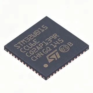
PN5190B1EV/C121Y - 13.56MHz NFC Frontend IC | NXP Semiconductors
MPN: PN5190B1EV-C121Y ✓ Active| Qty | Unit Price | Extended |
|---|---|---|
| 1 | $0 | $0.00 |
| 10 | $0 | $0.00 |
| 100 | $0 | $0.00 |
| 500 | $0 | $0.00 |
| 1,000 | $0 | $0.00 |
PN5190B1EV-C121Y Overview
An NFC frontend is a dedicated RF transceiver that generates the 13.56 MHz carrier, modulates and demodulates the contactless air interface, and offloads protocol handling from the host MCU. In the system hierarchy it sits below the application controller and above the antenna matching network, making it the physical layer of an NFC reader, POS terminal or access-control reader.
Key features include high RF output power for challenging RF environments, multi-protocol support covering EMVCo-relevant contactless schemes, SPI host interface, and factory initialization with firmware V2.7 supporting encrypted firmware download for secure field updates. NXP states the enhanced feature set simplifies EMVCo 3.0 certification, a major benefit for payment terminal makers.
Technically, the PN5190B1 (silicon version B1) requires firmware V2.0 or higher per the datasheet, and the C121Y suffix denotes the firmware/programming variant. The very-thin fine-pitch ball grid array keeps the RF section close to the antenna for superior RF performance in compact reader designs.
Typical applications include EMVCo payment terminals, physical access control readers, POS systems, and industrial or handheld NFC devices where difficult RF coupling must be handled reliably.
Design consideration: the delivered packaging is 13-inch reel, MSL 3, minimum order quantity 2450 pieces, so plan moisture handling and procurement volume accordingly.
This page synthesizes distributor inventory data, the NXP datasheet, and drop-in alternative analysis not found on any single distributor page.
Drop-in alternatives for PN5190B1EV-C121Y — same package, pin-to-pin compatible. Different-package parts requiring PCB rework are excluded.
Quick Comparison Tool — Select alternative parts for side-by-side comparison:
PN5190B0EV/C121Y
✅ Drop-In ⚠️ 参数待验证📋 Reference alternative (not in catalog)
PN5190B1EV/C121K
✅ Drop-In📋 Reference alternative (not in catalog)
PN5190B1EV/C121Y
✅ Drop-In📋 Reference alternative (not in catalog)
PN5190B1EV-C121Y Specifications
| Function | NFC Frontend / RFID Reader IC |
| Carrier Frequency | 13.56 MHz |
| Supported Standards | ISO 14443, ISO 15693, ISO 18000-3, ISO 18092, ISO 21481, FeliCa, MIFARE |
| Host Interface | SPI |
| Supply Voltage Range | 2.4 V to 6 V |
| Silicon Version | B1 |
| Factory Firmware | FW 2.7 (supports encrypted firmware download) |
| Minimum Firmware Requirement | V2.0 or higher |
| Package | VFBGA64 (SOT2062-1), 4.5 mm x 4.5 mm x 0.8 mm |
| Ball Count | 64 |
| Mounting Type | Surface Mount |
| Moisture Sensitivity Level | MSL 3 |
| Packaging | 13-inch reel, MOQ 2450 pcs |
| Target Applications | Payment (EMVCo 3.0), physical access control |
| RF Output Power | High output power for challenging RF environments |
| Certification Support | Simplifies EMVCo 3.0 certification |
PN5190B1EV-C121Y vfbga64 (sot2062-1), 4.5 mm x 4.5 mm x 0.8 mm Pin Configuration Guide
Pin configuration for PN5190B1EV-C121Y (vfbga64 (sot2062-1), 4.5 mm x 4.5 mm x 0.8 mm package). Pin numbering, functions, and connection diagrams are defined in the manufacturer datasheet. Refer to it for the exact footprint and soldering guidelines.

No detailed pinout data available for PN5190B1EV-C121Y.
Refer to the datasheet for full pin configuration.
Typical Applications
PN5190B1EV-C121Y is suitable for 6 applications: EMVCo Payment Terminals, Physical Access Control Readers, Handheld and Mobile NFC Devices, Industrial NFC and RFID Infrastructure, Smart Meters and Utility Infrastructure, Consumer IoT and Smart Home Hubs.
EMVCo Payment Terminals
The PN5190B1EV/C121Y fits payment terminal RF sections because its high 13.56 MHz RF output power sustains field strength at difficult card-coupling positions, and NXP explicitly states the feature set simplifies EMVCo 3.0 certification. In a typical POS design the PN5190 sits between the application MCU (connected via SPI at 2.4 V to 6 V supply) and the antenna matching network, running NXP firmware V2.0+ (delivered as FW 2.7 with encrypted download support). It handles ISO 14443 Type A/B, MIFARE and FeliCa card populations in one transceiver, so a single antenna path covers global contactless card schemes. The trade-off versus integrated-MCU NFC chips is the external host processor requirement, which in return gives terminal makers full control of the EMV kernel on a separate, certifiable processor.
Recommended
Physical Access Control Readers
Access control panels and door readers benefit from the PN5190B1EV/C121Y because its high RF output power achieves reliable read range with credentials presented at varying angles and distances, a common field failure mode for lower-power readers. The multi-protocol stack (ISO 14443, ISO 15693, ISO 18092, MIFARE) lets one reader serve MIFARE Classic/DESFire employee badges, ISO 15693 long-range cards, and NFC-enabled smartphones without hardware changes. Connected over SPI to a panel controller within the 2.4 V to 6 V supply range, the PN5190 offloads RF timing and framing while the host enforces credential policy. The compact 4.5 mm x 4.5 mm VFBGA64 package fits slim reader housings, and MSL 3 standard SMT assembly keeps manufacturing cost low for volume deployments.
Recommended
Handheld and Mobile NFC Devices
Battery-powered handheld scanners, inventory terminals and mobile payment devices suit the PN5190B1EV/C121Y because its 2.4 V to 6 V supply range operates directly from a single Li-ion cell (up to 4.2 V) or a boost converter rail, minimizing power-tree complexity. The SPI interface draws the digital section efficiently while the high-power RF stage can be enabled on demand for tag reads, keeping average battery drain low in duty-cycled applications. The very-thin 0.8 mm VFBGA64 package allows placement inside slim enclosures close to the antenna window, which improves coupling efficiency in handheld form factors. Firmware V2.7 with encrypted download lets OEMs update NFC behavior in the field, an important capability for devices with multi-year service lives deployed across changing card ecosystems.
Recommended
Industrial NFC and RFID Infrastructure
Industrial RFID gateways, tool-crib tracking stations and production-line authentication nodes use the PN5190B1EV/C121Y where metallic environments and cable runs create challenging RF conditions - exactly the scenario NXP targets with this frontend's high output power. ISO 15693 and ISO 18000-3 support enables shelf-tag and item-level inventory reads at longer range than ISO 14443 allows, while MIFARE and ISO 14443 handle operator badges and service tools. The SPI host link integrates cleanly with PLC-adjacent controllers, and the wide 2.4 V to 6 V input tolerates industrial supply variations. Because firmware is upgradeable via encrypted download (factory FW 2.7), integrators can adapt protocol behavior after deployment without recalling hardware, reducing total cost of ownership across multi-year industrial rollouts.
Recommended
Smart Meters and Utility Infrastructure
Smart electricity and water meters increasingly use NFC as a maintenance interface, and the PN5190B1EV/C121Y provides the RF layer for technician bring-up, firmware configuration and prepaid credit top-up via smartphone or service reader. The high output power maintains communication through meter enclosures that attenuate the 13.56 MHz field, and the multi-protocol support reads both utility-issued MIFARE/ISO 14443 media and ISO 15693 labels. Operating from 2.4 V to 6 V, the frontend matches common meter supply rails, while the SPI interface connects to the metering SoC with minimal GPIO cost. Encrypted firmware download (FW 2.7 delivered) aligns with utility security requirements, allowing the NFC firmware to be updated in the field without exposing proprietary images during meter service visits.
Recommended
Consumer IoT and Smart Home Hubs
Smart home hubs, Wi-Fi routers and set-top boxes use NFC pairing so users can tap a phone or tag to commission the device, and the PN5190B1EV/C121Y provides a robust RF frontend for this role. Its ISO 18092 and NFC Forum-relevant protocol support handles peer-to-peer and card-emulation interactions with Android and iOS devices, while the high output power compensates for plastic enclosures and antenna placements constrained by industrial design. The 2.4 V to 6 V supply and SPI host interface drop into typical 3.3 V consumer designs with minimal components, and the 4.5 mm x 4.5 mm x 0.8 mm VFBGA64 keeps the bill-of-materials footprint small on crowded main boards. FW 2.7 with encrypted download supports secure OTA refresh of the NFC stack over the product lifetime.
Recommended
Recommended Products Summary
Engineering reference data for PN5190B1EV-C121Y — comparison, design guidance, and compliance information.
Selection Guide
Comparison with Alternatives
| Parameter | This Product | PN5190B0EV/C121Y | PN5190B1EV/C121K | PN7462AUHN/C64X |
|---|---|---|---|---|
| Package | VFBGA64 (SOT2062-1), 4.5 mm x 4.5 mm x 0.8 mm | VFBGA64 (SOT2062-1) - same | VFBGA64 (SOT2062-1) - same | HVQFN-48 - different, not pin-compatible |
| Brand | NXP Semiconductors | NXP Semiconductors | NXP Semiconductors | NXP Semiconductors |
| Silicon Version | B1 | B0 (earlier step) | B1 | N/A (different product) |
| Host Interface | SPI | SPI | SPI | Integrated Cortex-M MCU (no external SPI host needed) |
| Protocols | ISO 14443/15693/18000-3/18092/21481, FeliCa, MIFARE | Same protocol set (firmware dependent) | Same protocol set | ISO 14443, ISO 15693, MIFARE, FeliCa |
Key Differentiators
- High RF output power for EMVCo-grade coupling (vs PN7462AUHN/C64X)
- Dedicated frontend architecture with encrypted firmware update (vs PN7462AUHN/C64X)
- Only true drop-ins are same-family variants - plan supply accordingly (vs PN5190B0EV/C121Y)
Design Notes
The SOT2062-1 VFBGA64 is a 0.8 mm-height very-thin fine-pitch BGA at 4.5 mm x 4.5 mm. Use a via-in-pad or dogbone fanout strategy on the 0.4 mm or finer ball pitch, and keep the RF antenna matching network within a few millimeters of the RF balls to minimize parasitics at 13.56 MHz. Follow the NXP PN5190 hardware design guide layout reference; NXP provides additional design-in documents separately from the public datasheet and these should be requested during schematic review.
Supply the PN5190B1 within its 2.4 V to 6 V specified range and decouple the RF power pins with low-ESR ceramic capacitors placed directly at the balls. Because the RF output stage draws pulsed load currents during 13.56 MHz carrier bursts, size the bulk capacitance to prevent supply droop that would distort the modulation index and risk EMVCo amplitude compliance. Estimate current demand from the antenna matching simulation, not from the digital supply figures.
The datasheet electrical specification is valid only for silicon B1 running firmware V2.0 or higher - designs based on early A0 silicon or older firmware may see different behavior. Confirm the ordered suffix (C121Y) matches your required firmware/programming configuration, and remember the part is MSL 3: respect the 168-hour floor life after opening the moisture-barrier bag, or bake per J-STD-033 before reflow. MOQ is 2450 pcs on 13-inch reels, so plan procurement volume accordingly.
Compliance Information
Provided distributor listings do not state RoHS/REACH/lead-free status. Verify on the official NXP PN5190B1EV product page or NXP compliance database before compliance-critical designs.