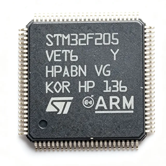
STM32F205VET6 - 120MHz ARM Cortex-M3 MCU, 512KB Flash | STMicroelectronics
MPN: STM32F205VET6 ✓ Active| Qty | Unit Price | Extended |
|---|---|---|
| 1 | $12.85 | $12.85 |
| 10 | $11.5 | $115.00 |
| 100 | $9.95 | $995.00 |
| 500 | $8.4 | $4,200.00 |
| 1,000 | $7.25 | $7,250.00 |
STM32F205VET6 Overview
A microcontroller (MCU) is a compact integrated circuit that combines a processor core, volatile and non-volatile memory, and programmable peripherals to govern a specific operation within an embedded system. MCUs sit in the hierarchy of embedded processors between simple 8-bit controllers and high-end application processors, and are optimized for deterministic real-time control and signal processing. The STM32F205VET6 specifically belongs to the ARM Cortex-M3 lineage (32-bit RISC core), positioning it above 8/16-bit microcontrollers in compute density while remaining below Cortex-A application processors in both cost and power.
Key features include 120 MHz maximum CPU frequency, 512KB on-chip Flash (512K x 8 organization), 132KB SRAM, 17 general-purpose and advanced-control timers, 3x 12-bit ADCs, USB OTG High-Speed and Full-Speed, on-chip 10/100 Ethernet MAC, 2x CAN, 3x SPI, 3x I2C, 5x USART/UART plus UART, and a digital camera interface. The adaptive real-time (ART) memory accelerator reduces Flash wait states to deliver close-to-zero penalty execution from on-chip code, and the part supports cryptographic features such as the unique 96-bit device ID and RNG in this density.
Technically, the STM32F205VET6 is fabricated on a low-power CMOS process and offers multiple low-power modes (Sleep, Stop, Standby) with fast wakeup times for battery-driven applications. The 100-pin LQFP package exposes 82 GPIOs tolerating 5V on most pins, includes an integrated voltage regulator for single-supply operation, and supports JTAG and SWD interfaces for in-circuit debug. Independent and window watchdog timers, a SysTick timer, and a real-time clock (RTC) with calendar and backup registers round out the on-chip resources.
Typical applications include industrial automation and motor control, building and home automation gateways, consumer HMI with TFT or camera input, USB peripherals, Ethernet-connected IoT nodes, medical instrumentation, and point-of-sale terminals. Its combination of high CPU throughput, on-chip Ethernet and USB OTG HS makes it especially attractive when designers need wired connectivity without an external PHY companion MCU.
When designing with this MCU, place decoupling capacitors (typically 100 nF + 4.7 uF) on each VDDA/VSS pair as close to the pins as the PCB layout allows, and route VBAT7 (VBAT) directly to a coin cell or supercap if RTC backup retention is required. Carefully observe BOOT0 pin configuration to select the correct boot source (main Flash, system memory bootloader, or embedded SRAM) and verify HSE/HSI clock tree values against the RM0033 reference manual before locking the firmware.
This page synthesizes distributor pricing snapshots, drop-in alternatives, and design guidance that are not collected in any single place in the manufacturer datasheet, providing a faster procurement and design start than reading the full RM0033 reference manual from scratch.
Drop-in alternatives for STM32F205VET6 — same package, pin-to-pin compatible. Different-package parts requiring PCB rework are excluded.
Variants in this series
Same-series models that are drop-in compatible with STM32F205VET6 (same form factor and footprint) — differing in Communication Interfaces, Package, Timers, Mounting Type, Operating Temperature.
Quick Comparison Tool — Select alternative parts for side-by-side comparison:
STM32F207VET6
✅ Drop-In ⚠️ Specs Unverified📋 Reference alternative (not in catalog)
STM32F205VCT6TR
✅ Drop-In ⚠️ Specs Unverified✓ In Stock
$7.95 / Unit
View Datasheet →STM32F405VET6
✅ Drop-In ⚠️ Specs Unverified📋 Reference alternative (not in catalog)
STM32F205VET6TR
✅ Drop-In ⚠️ Specs Unverified📋 Reference alternative (not in catalog)
STM32F205RET6
✅ Drop-In ⚠️ Specs Unverified✓ In Stock
$7.95 / Unit
View Datasheet →GD32F207VKT6
✅ Drop-In📋 Reference alternative (not in catalog)
STM32F205VET6 Maximum Ratings & Electrical Characteristics
| Core | ARM Cortex-M3 32-bit RISC |
| Maximum CPU Frequency | 120 MHz |
| DMIPS Performance | 150 DMIPS |
| Program Memory (Flash) | 512 KB (512K x 8) |
| RAM Size | 132 KB (132K x 8) |
| Number of I/O Pins | 82 |
| Package | 100-LQFP (14x14 mm) |
| Supply Voltage | 1.8 V to 3.6 V |
| Operating Temperature | -40 C to +85 C (industrial) |
| ADC | 3x 12-bit |
| Timers | 17 (general-purpose + advanced-control) |
| Communication Interfaces | 15 (SPI, I2C, USART/UART, CAN, USB OTG, Ethernet) |
| USB | USB OTG HS + USB OTG FS |
| Ethernet | 10/100 MAC on-chip |
| Camera Interface | Yes (8/10/12-bit parallel) |
| Mounting Type | Surface Mount |
| MSL Level | 3 (per JEDEC J-STD-020) |
| RoHS Status | Compliant |
STM32F205VET6 Pin Configuration
| Pin 1 | PE2 — GPIO PE2 / TRACECLK / SPI4 SCK |
| Pin 2 | PE3 — GPIO PE3 / TRACED0 |
| Pin 3 | PE4 — GPIO PE4 / TRACED1 |
| Pin 4 | PE5 — GPIO PE5 / TRACED2 |
| Pin 5 | PE6 — GPIO PE6 / TRACED3 |
| Pin 6 | VBAT — RTC backup battery supply |
| Pin 7 | PC13 — GPIO PC13 / RTC Tamper (anti-tamper) |
| Pin 8 | PC14 — GPIO PC14 / OSC32_IN (LSE crystal) |
| Pin 9 | PC15 — GPIO PC15 / OSC32_OUT (LSE crystal) |
| Pin 10 | VSS — Digital ground |
| Pin 11 | VDD — Digital supply (1.8V-3.6V) |
| Pin 12 | OSC_IN — HSE crystal in / external clock |
| Pin 13 | OSC_OUT — HSE crystal out |
| Pin 14 | NRST — Active-low reset input |
| Pin 15 | PC0 — GPIO PC0 / ADC123_IN10 |
| Pin 16 | PC1 — GPIO PC1 / ADC123_IN11 |
| Pin 17 | PC2 — GPIO PC2 / ADC123_IN12 |
| Pin 18 | PC3 — GPIO PC3 / ADC123_IN13 |
| Pin 19 | VSSA — Analog ground |
| Pin 20 | VDDA — Analog supply (1.8V-3.6V) |
| Pin 21 | PA0 — GPIO PA0 / WKUP / ADC123_IN0 / TIM2_CH1_ETR |
| Pin 22 | PA1 — GPIO PA1 / ADC123_IN1 / TIM2_CH2 |
| Pin 23 | PA2 — GPIO PA2 / ADC123_IN2 / TIM2_CH3 / USART2_TX |
| Pin 24 | PA3 — GPIO PA3 / ADC123_IN3 / TIM2_CH4 / USART2_RX |
| Pin 25 | VSS — Digital ground |
| Pin 26 | VDD — Digital supply |
| Pin 27 | PA4 — GPIO PA4 / ADC12_IN4 / SPI1_NSS / DAC_OUT1 |
| Pin 28 | PA5 — GPIO PA5 / ADC12_IN5 / SPI1_SCK / DAC_OUT2 |
| Pin 29 | PA6 — GPIO PA6 / ADC12_IN6 / SPI1_MISO / TIM13_CH1 |
| Pin 30 | PA7 — GPIO PA7 / ADC12_IN7 / SPI1_MOSI / TIM14_CH1 |
| Pin 31 | PC4 — GPIO PC4 / ADC12_IN14 |
| Pin 32 | PC5 — GPIO PC5 / ADC12_IN15 |
| Pin 33 | PB0 — GPIO PB0 / ADC12_IN8 / TIM1_CH2N |
| Pin 34 | PB1 — GPIO PB1 / ADC12_IN9 / TIM1_CH3N |
| Pin 35 | PB2 — GPIO PB2 / BOOT1 |
| Pin 36 | PE7 — GPIO PE7 / TIM1_ETR |
| Pin 37 | PE8 — GPIO PE8 / TIM1_CH1N |
| Pin 38 | PE9 — GPIO PE9 / TIM1_CH1 |
| Pin 39 | PE10 — GPIO PE10 / TIM1_CH2N |
| Pin 40 | PE11 — GPIO PE11 / TIM1_CH2 |
| Pin 41 | PE12 — GPIO PE12 / TIM1_CH3N |
| Pin 42 | PE13 — GPIO PE13 / TIM1_CH3 |
| Pin 43 | PE14 — GPIO PE14 / TIM1_CH4 |
| Pin 44 | PE15 — GPIO PE15 / TIM1_BKIN |
| Pin 45 | PB10 — GPIO PB10 / I2C2_SCL / USART3_TX / TIM2_CH3 |
| Pin 46 | PB11 — GPIO PB11 / I2C2_SDA / USART3_RX / TIM2_CH4 |
| Pin 47 | VSS — Digital ground |
| Pin 48 | VDD — Digital supply |
| Pin 49 | PB12 — GPIO PB12 / SPI2_NSS / I2S2_WS / TIM1_BKIN |
| Pin 50 | PB13 — GPIO PB13 / SPI2_SCK / I2S2_CK / TIM1_CH1N |
| Pin 51 | PB14 — GPIO PB14 / SPI2_MISO / TIM1_CH2N |
| Pin 52 | PB15 — GPIO PB15 / SPI2_MOSI / TIM1_CH3N |
| Pin 53 | PD8 — GPIO PD8 / USART3_TX |
| Pin 54 | PD9 — GPIO PD9 / USART3_RX |
| Pin 55 | PD10 — GPIO PD10 |
| Pin 56 | PD11 — GPIO PD11 |
| Pin 57 | PD12 — GPIO PD12 / TIM4_CH1 |
| Pin 58 | PD13 — GPIO PD13 / TIM4_CH2 |
| Pin 59 | VSS — Digital ground |
| Pin 60 | VDD — Digital supply |
| Pin 61 | PD14 — GPIO PD14 / TIM4_CH3 |
| Pin 62 | PD15 — GPIO PD15 / TIM4_CH4 |
| Pin 63 | PC6 — GPIO PC6 / TIM8_CH1 / USART6_TX |
| Pin 64 | PC7 — GPIO PC7 / TIM8_CH2 / USART6_RX |
| Pin 65 | PC8 — GPIO PC8 / TIM8_CH3 |
| Pin 66 | PC9 — GPIO PC9 / TIM8_CH4 |
| Pin 67 | PA8 — GPIO PA8 / USART1_CK / TIM1_CH1 / MCO1 |
| Pin 68 | PA9 — GPIO PA9 / USART1_TX / TIM1_CH2 |
| Pin 69 | PA10 — GPIO PA10 / USART1_RX / TIM1_CH3 |
| Pin 70 | PA11 — GPIO PA11 / CAN1_RX / USBDM / TIM1_CH1N |
| Pin 71 | PA12 — GPIO PA12 / CAN1_TX / USBDP / TIM1_CH2N |
| Pin 72 | PA13 — GPIO PA13 / JTMS / SWDIO |
| Pin 73 | VCAP_1 — Internal regulator 1.2V decoupling |
| Pin 74 | VSS — Digital ground |
| Pin 75 | VDD — Digital supply |
| Pin 76 | PA14 — GPIO PA14 / JTCK / SWCLK |
| Pin 77 | PA15 — GPIO PA15 / JTDI / SPI3_NSS / I2S3_WS |
| Pin 78 | PC10 — GPIO PC10 / SPI3_SCK / I2S3_CK / USART3_TX |
| Pin 79 | PC11 — GPIO PC11 / SPI3_MISO / I2S3_ext_SD / USART3_RX |
| Pin 80 | PC12 — GPIO PC12 / SPI3_MOSI / I2S3_SD / USART3_CK |
| Pin 81 | PD0 — GPIO PD0 / CAN1_RX |
| Pin 82 | PD1 — GPIO PD1 / CAN1_TX |
| Pin 83 | PD2 — GPIO PD2 / TIM3_ETR |
| Pin 84 | PD3 — GPIO PD3 / USART2_CTS |
| Pin 85 | PD4 — GPIO PD4 / USART2_RTS |
| Pin 86 | PD5 — GPIO PD5 / USART2_TX |
| Pin 87 | PD6 — GPIO PD6 / USART2_RX |
| Pin 88 | PD7 — GPIO PD7 / USART2_CK |
| Pin 89 | PB3 — GPIO PB3 / JTDO / SPI3_SCK / I2S3_CK / TIM2_CH2 |
| Pin 90 | PB4 — GPIO PB4 / NJTRST / SPI3_MISO |
| Pin 91 | PB5 — GPIO PB5 / I2C1_SMBAI |
| Pin 92 | PB6 — GPIO PB6 / I2C1_SCL / TIM4_CH1 |
| Pin 93 | PB7 — GPIO PB7 / I2C1_SDA / TIM4_CH2 |
| Pin 94 | BOOT0 — Boot mode select (0=main Flash, 1=system bootloader) |
| Pin 95 | PB8 — GPIO PB8 / TIM4_CH3 |
| Pin 96 | PB9 — GPIO PB9 / TIM4_CH4 |
| Pin 97 | PE0 — GPIO PE0 / TIM4_ETR |
| Pin 98 | PE1 — GPIO PE1 |
| Pin 99 | VSS — Digital ground |
| Pin 100 | VDD — Digital supply |
Typical Applications
STM32F205VET6 is suitable for 7 applications: Industrial Motor Control, Industrial Ethernet Gateway, USB OTG HS Peripheral, Building Automation HMI, Medical Point-of-Care Device, Camera-Enabled Embedded Vision, Power-Metering / Data Logger.
Industrial Motor Control
The STM32F205VET6's 120 MHz Cortex-M3 core with 150 DMIPS throughput handles real-time field-oriented control (FOC) loops for three-phase PMSM and BLDC motors, while the 17 timers including advanced-control PWM timers (TIM1/TIM8) generate the six-step or space-vector PWM needed for 3-phase inverter drives. The three 12-bit ADCs sample phase currents at sub-microsecond rates for closed-loop torque control. The 100-LQFP package exposes 82 GPIO pins, providing ample routing for encoder, Hall-sensor and gate-driver interfaces. Industrial design wins typically pair this MCU with the STGAP1AS gate-driver and the IGBT or MOSFET power stage, using the on-chip Cortex-M3 to execute state machines while a separate STM32 runs HMI.
Recommended
Industrial Ethernet Gateway
On-chip 10/100 Ethernet MAC with MII/RMII interface lets the STM32F205VET6 act as an Ethernet gateway in industrial-automation networks, pairing with an external PHY such as the LAN8720A or DP83848 to provide full TCP/IP or PROFINET/EtherNet-IP connectivity. The 512 KB Flash stores the full TCP/IP stack (lwIP or RT-Thread) plus an industrial protocol library, and the 132 KB SRAM buffers multiple sockets. Hardware enable pins, 5 V-tolerant I/O and the industrial -40 C to +85 C temperature range suit DIN-rail mounted controllers. Reference designs typically route RMII to the LAN8720A PHY plus an RJ45 with integrated magnetics for two-port industrial Ethernet gateways.
Recommended
USB OTG HS Peripheral
The STM32F205VET6's on-chip USB OTG High-Speed and Full-Speed controllers plus 8 KB USB-on-DSRP SRAM enable it to act as either a USB device or host, ideal for industrial data loggers, POS terminals, and medical peripherals that stream high-speed data over USB. USB OTG HS supports up to 480 Mbps when paired with an external ULPI PHY such as the USB3300, while the integrated FS OTG controller handles 12 Mbps directly. Combined with the 512 KB Flash for the USB device/host stack and 132 KB SRAM for endpoint buffers, designers can implement CDC, HID, MSC, and vendor-class devices without an external companion chip.
Recommended
Building Automation HMI
The 82 GPIO pins and 15 communication interfaces of the STM32F205VET6 make it ideal for HMI panels in building-automation controllers, supporting keypads, character or graphic LCDs, and capacitive-touch sliders via I2C or SPI touch controllers. The on-chip timers drive PWM-controlled backlight dimming while a UART interfaces to a wireless module for KNX-RF or LoRa connectivity. The 132 KB SRAM supports a graphical UI library without external memory, and the wide 1.8V-3.6V supply simplifies designs powered from 24 V industrial bus rails via a step-down converter. Reference designs integrate RS-485 transceivers on USART for BACnet or Modbus backbone connectivity.
Recommended
Medical Point-of-Care Device
Medical point-of-care devices benefit from the STM32F205VET6's three 12-bit ADCs (with up to 24 channels total) for multi-signal biosensor acquisition, 132 KB SRAM to buffer sample streams, and USB OTG HS for fast data upload to a host analyzer. The Cortex-M3 at 120 MHz executes digital signal processing for pulse oximetry, glucose metering, or ECG front-end filtering in real time. The industrial temperature range and 5 V-tolerant I/O support battery-charging ICs directly. Reference designs combine an AFE such as the ADS1292 for ECG front-end plus an FTDI or direct USB link for medical-grade data transfer.
Recommended
Camera-Enabled Embedded Vision
The STM32F205VET6 integrates a parallel 8/10/12-bit digital camera interface (DCMI) that streams from external CMOS sensors up to VGA-class resolution into the 132 KB SRAM buffer for image-processing pipelines. The 120 MHz Cortex-M3 plus ART accelerator handles simple barcode reading, QR scanning, or pre-DSP pre-processing before forwarding compressed JPEG data over USB or Ethernet. For higher-resolution designs the STM32F7 or STM32H7 families are recommended, but for low-cost VisoLation the F205VET6 is a strong choice. Typical designs pair this MCU with an OV2640A6 or OV7670 sensor and store images to an external SPI flash.
Recommended
Power-Metering / Data Logger
In three-phase power metering and remote data loggers the STM32F205VET6's three 12-bit ADCs simultaneously sample voltage and current channels while its 17 timers drive zero-crossing detection and pulse counting. The Ethernet MAC streams metering data to a remote SCADA, while SD-card interface (SPI-mode) on the F205/F207 allows local buffering of outage logs. The 132 KB SRAM supports a 100 ms metering window with multi-rate buffer. Reference implementations use the STM32 DSP library for FFT-based harmonic analysis and a real-time clock (RTC) for time-stamping events with backup-battery retention across power cycles.
Recommended
Recommended Products Summary
Engineering reference data for STM32F205VET6 — comparison, design guidance, and compliance information.
Selection Guide
Comparison with Alternatives
| Parameter | This Product | STM32F207VET6 | STM32F205VCT6 | STM32F405VET6 | STM32F205VET6TR | STM32F205RET6 | GD32F207VKT6 |
|---|---|---|---|---|---|---|---|
| Brand | STMicroelectronics | STMicroelectronics | STMicroelectronics | STMicroelectronics | STMicroelectronics | STMicroelectronics | GigaDevice |
| Package | 100-LQFP (14x14) | 100-LQFP (14x14) | 100-LQFP (14x14) | 100-LQFP (14x14) | 100-LQFP (14x14) | 64-LQFP (10x10) | 100-LQFP (14x14) |
| Core | ARM Cortex-M3 | ARM Cortex-M3 | ARM Cortex-M3 | ARM Cortex-M4F | ARM Cortex-M3 | ARM Cortex-M3 | ARM Cortex-M3 |
| Max CPU Frequency | 120 MHz | 120 MHz | 120 MHz | 168 MHz | 120 MHz | 120 MHz | 120 MHz |
| Flash | 512 KB | 512 KB | 256 KB | 512 KB | 512 KB | 512 KB | 3 MB |
| SRAM | 132 KB | 132 KB | 96 KB | 192 KB | 132 KB | 64 KB | 256 KB |
| GPIO Count | 82 | 82 | 82 | 82 | 82 | 51 | 82 |
| Operating Temperature | -40 C to +85 C | -40 C to +85 C | -40 C to +85 C | -40 C to +85 C | -40 C to +85 C | -40 C to +85 C | -40 C to +85 C |
| Ethernet MAC | Yes | Yes | Yes | Yes | Yes | Yes | Yes |
| Approx Unit Price (USD, qty 1) | 12.85 | ~14.50 | ~10.50 | ~15.00 | ~12.85 | ~10.50 | ~5.50 |
Key Differentiators
- Highest Flash density in STM32F2 120 MHz family at 100-LQFP footprint (vs STM32F205VCT6)
- Same peripherals as F207 without added crypto/SDMMC cost overhead (vs STM32F207VET6)
- Cortex-M3 simplicity with no FPU/DSP that can complicate hard-real-time scheduling (vs STM32F405VET6)
- Lower unit cost than F405/F207 with identical pinout and peripherals (vs GD32F207VKT6)
Design Notes
Decouple each VDD/VSS pair with a 100 nF X7R ceramic placed within 5 mm of the pin, and add a 4.7 uF bulk capacitor per supply rail. VDDA must be tied to VDD through a ferrite bead or short trace if ADC accuracy matters, and the VCAP_1 pin (pin 73) must be left floating with a 100 nF + 1 uF pair to ground for the internal 1.2 V regulator. Estimated: based on standard ST reference designs for the STM32F2 family; values are typical, not datasheet-maximum.
The 100-LQFP package has a typical theta_JA around 50 C/W on a 2-layer JEDEC test board. At 120 MHz with all peripherals active the F205 draws roughly 50-80 mA from VDD, so under standard lab conditions the junction rises only 5-10 C above ambient. Estimated: based on typical STM32F205 datasheet current-consumption tables and LQFP-100 thermal resistance; verify with on-board measurements in the final design.
Route the HSE/OSCIN/PH0 and HSE/OSCOUT/PH1 traces as short, symmetric, length-matched differential pairs to the external crystal or oscillator to avoid start-up issues; place the load capacitors within 2 mm of the crystal. The USB OTG FS data lines (PA11/PA12 or PB14/PB15 depending on remap) require 90 ohm differential impedance plus series matching resistors. For Ethernet, the MII/RMII traces to the external PHY must be length-matched within 50 mil and routed over a continuous ground plane.
Always configure the BOOT0 pin through a 10 kohm pull-down to select main-Flash boot; leaving it floating can result in unpredictable boot. The NRST pin must be pulled up with 100 nF in parallel to VDD, otherwise the MCU can lock up on noisy power-up. Do not drive 5 V into any non-5V-tolerant pin (notably PH2, PA13/14, BOOT0) or you will permanently damage the part. Always unlock the backup-Domain with the correct RCC sequence before modifying RTC registers or VBAT-mode SRAM.
The camera interface (DCMI) and external SDRAM bus, when used, must be routed with controlled-impedance traces (typically 50 ohm single-ended) and a continuous reference ground plane. Series-stubs should be avoided on the camera PCLK line; use point-to-point routing from sensor to MCU with the trace length less than 50 mm. Place a 33 ohm series damping resistor close to the MCU side if the sensor sits more than 25 mm away.
Compliance Information
Industrial-grade STM32F2 parts are not AEC-Q100 qualified; for automotive applications use the STM32F2x5/F2x7 with -A suffix (e.g., STM32F205VET6A). ST product page states RoHS, REACH, and conflict-mineral compliance.