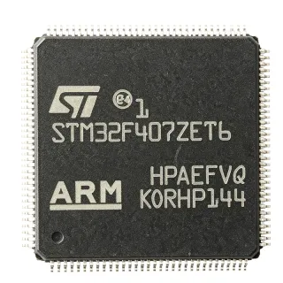
STM32F205ZET6 - 32-bit ARM Cortex-M3 MCU, 512KB Flash | STMicroelectronics
MPN: STM32F205ZET6 ✓ Active| Qty | Unit Price | Extended |
|---|---|---|
| 1 | $12.5 | $12.50 |
| 10 | $11.2 | $112.00 |
| 100 | $9.8 | $980.00 |
| 500 | $8.9 | $4,450.00 |
| 1,000 | $8.1 | $8,100.00 |
STM32F205ZET6 Overview
What is a microcontroller? A microcontroller (MCU) is a compact integrated circuit designed to govern a specific operation in an embedded system. It integrates a processor core, memory (Flash and SRAM), and programmable input/output peripherals on a single chip. Microcontrollers are the backbone of embedded systems, enabling control, monitoring, and communication in applications ranging from consumer electronics to industrial automation. The STM32F205ZET6 belongs to the STM32F2 series, which is part of the broader STM32 family of 32-bit Flash microcontrollers based on the ARM Cortex-M processor. This family hierarchy positions the STM32F205ZET6 as a high-performance MCU with advanced connectivity and rich analog peripherals.
Key features of the STM32F205ZET6 include a 32-bit ARM Cortex-M3 CPU with adaptive real-time accelerator (ART) allowing 0-wait state execution from Flash, a memory protection unit (MPU), and a comprehensive set of peripherals. It offers up to 114 I/O ports, 3x 12-bit ADCs, 2x DACs, 12-bit timers, and advanced communication interfaces including USB 2.0 OTG HS/FS, Ethernet MAC, CAN, SPI, I2C, USART, and SDIO. The device operates from a 1.8V to 3.6V power supply and supports a temperature range of -40°C to +85°C (industrial grade).
Technically, the STM32F205ZET6 is built on a 90nm process technology, enabling high clock speeds with low power consumption. It includes a nested vectored interrupt controller (NVIC) for efficient interrupt handling, a DMA controller with 16 channels, and a true random number generator (RNG). The device also features a real-time clock (RTC) with calendar and alarm functions, and a flexible static memory controller (FSMC) for external memory expansion.
Typical applications include industrial control systems, motor drives, medical devices, consumer electronics, and IoT gateways. Its rich connectivity and high processing power make it ideal for applications requiring real-time control and communication, such as PLCs, robotics, and smart home hubs.
When designing with the STM32F205ZET6, ensure proper decoupling of the power supply pins with 100nF capacitors placed close to each VDD pin, and a 4.7uF bulk capacitor. The VDDA pin should be connected to a clean analog supply to minimize noise in ADC conversions. Also, configure the boot pins correctly to select the desired boot mode (Flash, SRAM, or system memory) for programming and debugging.
Drop-in alternatives for STM32F205ZET6 — same package, pin-to-pin compatible. Different-package parts requiring PCB rework are excluded.
Variants in this series
Same-series models that are drop-in compatible with STM32F205ZET6 (same form factor and footprint) — differing in ADC, DMA.
Quick Comparison Tool — Select alternative parts for side-by-side comparison:
STM32F207ZET6
✅ Drop-In✓ In Stock
$8.1 / Unit
View Datasheet →STM32F205ZGT6
✅ Drop-In📋 Reference alternative (not in catalog)
STM32F205ZET6 Maximum Ratings & Electrical Characteristics
| Core | ARM Cortex-M3 |
| Max Clock Speed | 120 MHz |
| Flash Memory | 512 KB |
| SRAM | 128 KB |
| Package | LQFP144 (20x20 mm) |
| Supply Voltage | 1.8V to 3.6V |
| Operating Temperature | -40°C to +85°C |
| GPIO Pins | 114 |
| ADC | 3x 12-bit, 24 channels |
| DAC | 2x 12-bit |
| Timers | 12x 16-bit, 2x 32-bit |
| Communication Interfaces | USB 2.0 OTG HS/FS, Ethernet MAC, CAN, SPI, I2C, USART, SDIO |
| DMA | 16 channels |
| RTC | Yes |
| RoHS | Compliant |
STM32F205ZET6 Pin Configuration
| Pin 1 | PE2 — GPIO / FSMC_A23 |
| Pin 2 | PE3 — GPIO / FSMC_A19 |
| Pin 3 | PE4 — GPIO / FSMC_A20 |
| Pin 4 | PE5 — GPIO / FSMC_A21 |
| Pin 5 | PE6 — GPIO / FSMC_A22 |
| Pin 6 | VBAT — Backup battery supply |
| Pin 7 | PC13 — GPIO / RTC_TAMP1 |
| Pin 8 | PC14 — GPIO / OSC32_IN |
| Pin 9 | PC15 — GPIO / OSC32_OUT |
| Pin 10 | PF0 — GPIO / FSMC_A0 |
| Pin 11 | PF1 — GPIO / FSMC_A1 |
| Pin 12 | PF2 — GPIO / FSMC_A2 |
| Pin 13 | PF3 — GPIO / FSMC_A3 |
| Pin 14 | PF4 — GPIO / FSMC_A4 |
| Pin 15 | PF5 — GPIO / FSMC_A5 |
| Pin 16 | VSS — Ground |
| Pin 17 | VDD — Power supply |
| Pin 18 | PF6 — GPIO / FSMC_NIORD |
| Pin 19 | PF7 — GPIO / FSMC_NREG |
| Pin 20 | PF8 — GPIO / FSMC_NIOWR |
| Pin 21 | PF9 — GPIO / FSMC_CD |
| Pin 22 | PF10 — GPIO / FSMC_INTR |
| Pin 23 | PF11 — GPIO / FSMC_NCE4_1 |
| Pin 24 | PF12 — GPIO / FSMC_NCE4_2 |
| Pin 25 | PF13 — GPIO / FSMC_A6 |
| Pin 26 | PF14 — GPIO / FSMC_A7 |
| Pin 27 | PF15 — GPIO / FSMC_A8 |
| Pin 28 | PG0 — GPIO / FSMC_A9 |
| Pin 29 | PG1 — GPIO / FSMC_A10 |
| Pin 30 | PG2 — GPIO / FSMC_A11 |
| Pin 31 | PG3 — GPIO / FSMC_A12 |
| Pin 32 | PG4 — GPIO / FSMC_A13 |
| Pin 33 | PG5 — GPIO / FSMC_A14 |
| Pin 34 | VSS — Ground |
| Pin 35 | VDD — Power supply |
| Pin 36 | PG6 — GPIO / FSMC_NE1 |
| Pin 37 | PG7 — GPIO / FSMC_NE2 |
| Pin 38 | PG8 — GPIO / FSMC_NCE3 |
| Pin 39 | PG9 — GPIO / FSMC_NE3 |
| Pin 40 | PG10 — GPIO / FSMC_NE4 |
| Pin 41 | PG11 — GPIO / FSMC_NCE4_1 |
| Pin 42 | PG12 — GPIO / FSMC_NE4 |
| Pin 43 | PG13 — GPIO / FSMC_A24 |
| Pin 44 | PG14 — GPIO / FSMC_A25 |
| Pin 45 | PG15 — GPIO / FSMC_A26 |
| Pin 46 | PD0 — GPIO / FSMC_D2 |
| Pin 47 | PD1 — GPIO / FSMC_D3 |
| Pin 48 | PD2 — GPIO / FSMC_D4 |
| Pin 49 | PD3 — GPIO / FSMC_D5 |
| Pin 50 | PD4 — GPIO / FSMC_D6 |
| Pin 51 | PD5 — GPIO / FSMC_D7 |
| Pin 52 | PD6 — GPIO / FSMC_D8 |
| Pin 53 | PD7 — GPIO / FSMC_D9 |
| Pin 54 | VSS — Ground |
| Pin 55 | VDD — Power supply |
| Pin 56 | PD8 — GPIO / FSMC_D10 |
| Pin 57 | PD9 — GPIO / FSMC_D11 |
| Pin 58 | PD10 — GPIO / FSMC_D12 |
| Pin 59 | PD11 — GPIO / FSMC_D13 |
| Pin 60 | PD12 — GPIO / FSMC_D14 |
| Pin 61 | PD13 — GPIO / FSMC_D15 |
| Pin 62 | PD14 — GPIO / FSMC_D0 |
| Pin 63 | PD15 — GPIO / FSMC_D1 |
| Pin 64 | PC0 — GPIO / ADC123_IN10 |
| Pin 65 | PC1 — GPIO / ADC123_IN11 |
| Pin 66 | PC2 — GPIO / ADC123_IN12 |
| Pin 67 | PC3 — GPIO / ADC123_IN13 |
| Pin 68 | VSSA — Analog ground |
| Pin 69 | VREF- — Negative reference voltage |
| Pin 70 | VDDA — Analog power supply |
| Pin 71 | VREF+ — Positive reference voltage |
| Pin 72 | PC4 — GPIO / ADC12_IN14 |
| Pin 73 | PC5 — GPIO / ADC12_IN15 |
| Pin 74 | PB2 — GPIO / BOOT1 |
| Pin 75 | PE7 — GPIO / FSMC_D4 |
| Pin 76 | PE8 — GPIO / FSMC_D5 |
| Pin 77 | PE9 — GPIO / FSMC_D6 |
| Pin 78 | PE10 — GPIO / FSMC_D7 |
| Pin 79 | PE11 — GPIO / FSMC_D8 |
| Pin 80 | PE12 — GPIO / FSMC_D9 |
| Pin 81 | PE13 — GPIO / FSMC_D10 |
| Pin 82 | PE14 — GPIO / FSMC_D11 |
| Pin 83 | PE15 — GPIO / FSMC_D12 |
| Pin 84 | PB10 — GPIO / I2C2_SCL / USART3_TX |
| Pin 85 | PB11 — GPIO / I2C2_SDA / USART3_RX |
| Pin 86 | VSS — Ground |
| Pin 87 | VDD — Power supply |
| Pin 88 | PB12 — GPIO / SPI2_NSS / I2C2_SMBA |
| Pin 89 | PB13 — GPIO / SPI2_SCK |
| Pin 90 | PB14 — GPIO / SPI2_MISO |
| Pin 91 | PB15 — GPIO / SPI2_MOSI |
| Pin 92 | PD8 — GPIO / USART3_TX |
| Pin 93 | PD9 — GPIO / USART3_RX |
| Pin 94 | PD10 — GPIO / USART3_CK |
| Pin 95 | PD11 — GPIO / USART3_CTS |
| Pin 96 | PD12 — GPIO / USART3_RTS |
| Pin 97 | PD13 — GPIO / USART3_CTS |
| Pin 98 | PD14 — GPIO / USART3_RTS |
| Pin 99 | PD15 — GPIO / USART3_CK |
| Pin 100 | PC6 — GPIO / I2S2_MCK / SDIO_D6 |
| Pin 101 | PC7 — GPIO / I2S2_MCK / SDIO_D7 |
| Pin 102 | PC8 — GPIO / SDIO_D0 |
| Pin 103 | PC9 — GPIO / SDIO_D1 |
| Pin 104 | PA8 — GPIO / USB_OTG_FS_SOF / I2C3_SCL |
| Pin 105 | PA9 — GPIO / USB_OTG_FS_VBUS / USART1_TX |
| Pin 106 | PA10 — GPIO / USB_OTG_FS_ID / USART1_RX |
| Pin 107 | PA11 — GPIO / USB_OTG_FS_DM / USART1_CTS |
| Pin 108 | PA12 — GPIO / USB_OTG_FS_DP / USART1_RTS |
| Pin 109 | PA13 — GPIO / SWDIO / JTMS |
| Pin 110 | VSS — Ground |
| Pin 111 | VDD — Power supply |
| Pin 112 | PA14 — GPIO / SWCLK / JTCK |
| Pin 113 | PA15 — GPIO / JTDI / SPI3_NSS |
| Pin 114 | PC10 — GPIO / SDIO_D2 |
| Pin 115 | PC11 — GPIO / SDIO_D3 |
| Pin 116 | PC12 — GPIO / SDIO_CK |
| Pin 117 | PD0 — GPIO / FSMC_D2 |
| Pin 118 | PD1 — GPIO / FSMC_D3 |
| Pin 119 | PD2 — GPIO / FSMC_D4 |
| Pin 120 | PD3 — GPIO / FSMC_D5 |
| Pin 121 | PD4 — GPIO / FSMC_D6 |
| Pin 122 | PD5 — GPIO / FSMC_D7 |
| Pin 123 | PD6 — GPIO / FSMC_D8 |
| Pin 124 | PD7 — GPIO / FSMC_D9 |
| Pin 125 | PE0 — GPIO / FSMC_NBL0 |
| Pin 126 | PE1 — GPIO / FSMC_NBL1 |
| Pin 127 | PE2 — GPIO / FSMC_A23 |
| Pin 128 | PE3 — GPIO / FSMC_A19 |
| Pin 129 | PE4 — GPIO / FSMC_A20 |
| Pin 130 | PE5 — GPIO / FSMC_A21 |
| Pin 131 | PE6 — GPIO / FSMC_A22 |
| Pin 132 | VSS — Ground |
| Pin 133 | VDD — Power supply |
| Pin 134 | PB3 — GPIO / JTDO / SPI3_SCK |
| Pin 135 | PB4 — GPIO / NJTRST / SPI3_MISO |
| Pin 136 | PB5 — GPIO / SPI3_MOSI / I2C1_SMBA |
| Pin 137 | PB6 — GPIO / I2C1_SCL / USART1_TX |
| Pin 138 | PB7 — GPIO / I2C1_SDA / USART1_RX |
| Pin 139 | BOOT0 — Boot mode selection |
| Pin 140 | PB8 — GPIO / I2C1_SCL / CAN1_RX |
| Pin 141 | PB9 — GPIO / I2C1_SDA / CAN1_TX |
| Pin 142 | PE7 — GPIO / FSMC_D4 |
| Pin 143 | PE8 — GPIO / FSMC_D5 |
| Pin 144 | PE9 — GPIO / FSMC_D6 |
Typical Applications
STM32F205ZET6 is suitable for 6 applications: Industrial Control Systems, Medical Devices, IoT Gateways, Consumer Electronics, Automotive Electronics, Test and Measurement Equipment.
Industrial Control Systems
The STM32F205ZET6 is ideal for industrial control systems such as PLCs, motor drives, and robotics. Its 120 MHz Cortex-M3 core provides fast processing for real-time control loops, while the advanced timers generate precise PWM signals for motor control. The multiple communication interfaces (CAN, USART, SPI, I2C) enable seamless integration with industrial networks like Modbus and CANopen. The device's wide supply voltage range and industrial temperature rating (-40°C to +85°C) ensure reliable operation in harsh environments. In a typical PLC application, the STM32F205ZET6 handles digital I/O scanning, analog input acquisition via its 12-bit ADCs, and communication with HMI panels over RS-485. The 512 KB Flash allows storing complex control algorithms and communication stacks, while the 128 KB SRAM supports real-time data buffering. The FSMC interface can be used to expand external memory for data logging. Overall, the STM32F205ZET6 offers a cost-effective solution for high-performance industrial controllers.
Recommended
Medical Devices
The STM32F205ZET6 is well-suited for medical devices such as patient monitors, infusion pumps, and diagnostic equipment. Its high processing power enables real-time signal processing for ECG, SpO2, and blood pressure monitoring. The device's multiple ADCs can simultaneously sample multiple physiological signals, while the DMA controller offloads data transfer to reduce CPU load. The USB 2.0 OTG interface allows connectivity to host computers for data logging and firmware updates. The low-power modes help extend battery life in portable devices. In a patient monitor, the STM32F205ZET6 acquires ECG signals via its 12-bit ADC at 1 kHz sampling rate, processes them using digital filters, and displays the waveform on an LCD. The device's reliability and long-term availability make it suitable for medical applications requiring regulatory compliance. The 512 KB Flash provides ample space for firmware implementing medical algorithms and communication protocols.
Recommended
IoT Gateways
The STM32F205ZET6 is an excellent choice for IoT gateways that aggregate data from multiple sensors and communicate with cloud services. Its rich connectivity options, including Ethernet (via external PHY), USB, CAN, and UART, allow it to interface with various sensor networks. The 120 MHz Cortex-M3 core can handle protocol stacks like MQTT, CoAP, and TLS encryption. The device's large Flash and SRAM support running an RTOS and multiple communication stacks simultaneously. In a typical IoT gateway, the STM32F205ZET6 collects data from Zigbee or LoRa modules via UART/SPI, processes it, and forwards it to the cloud over Ethernet or Wi-Fi (via external module). The low-power modes enable battery-powered operation in remote locations. The device's security features, including a true random number generator (RNG) and hardware CRC, enhance data security. The STM32F205ZET6's long-term availability and industrial temperature range make it suitable for outdoor IoT deployments.
Recommended
Consumer Electronics
The STM32F205ZET6 is used in consumer electronics such as smart home hubs, wearable devices, and audio equipment. Its high performance enables rich user interfaces with graphical displays, while its low-power modes extend battery life in portable devices. The device's USB OTG interface supports connection to smartphones and PCs for data transfer and charging. In a smart home hub, the STM32F205ZET6 manages Zigbee, Z-Wave, and Wi-Fi communication, controls smart devices, and provides a local automation engine. The 512 KB Flash allows storing complex automation rules and device profiles. The device's multiple timers and PWM outputs can drive LEDs and buzzers for user feedback. The STM32F205ZET6's cost-effectiveness and wide availability make it a popular choice for high-volume consumer products.
Recommended
Automotive Electronics
The STM32F205ZET6 is suitable for automotive applications such as body control modules, infotainment systems, and advanced driver-assistance systems (ADAS). Its high processing power and rich peripherals enable real-time control and communication in vehicles. The device's CAN interface supports communication with other ECUs in the vehicle network. The wide supply voltage range and industrial temperature rating ensure reliable operation in automotive environments. In a body control module, the STM32F205ZET6 controls lighting, windows, and door locks, while communicating over CAN. The device's multiple ADCs can monitor analog sensors for temperature and voltage. The 512 KB Flash provides ample space for automotive-grade firmware. While the STM32F205ZET6 is not AEC-Q100 qualified, it is often used in non-safety-critical automotive applications. For safety-critical applications, consider the STM32F2 series with AEC-Q100 qualification.
Recommended
Test and Measurement Equipment
The STM32F205ZET6 is used in test and measurement equipment such as oscilloscopes, data loggers, and signal generators. Its high-speed ADCs and DACs enable precise signal acquisition and generation. The device's DMA controller allows continuous data streaming without CPU intervention, enabling high-speed data capture. The USB interface provides connectivity to PCs for data analysis and remote control. In a portable data logger, the STM32F205ZET6 samples analog signals at high rates, stores data in external memory via FSMC, and transfers it to a PC over USB. The device's multiple timers can generate precise trigger signals for synchronized measurements. The 512 KB Flash allows storing complex measurement algorithms and calibration data. The STM32F205ZET6's performance and flexibility make it a popular choice for custom test equipment.
Recommended
Recommended Products Summary
Engineering reference data for STM32F205ZET6 — comparison, design guidance, and compliance information.
Selection Guide
Comparison with Alternatives
| Parameter | This Product | STM32F207ZET6 | STM32F205ZGT6 | STM32F205VET6 | LPC1768FBD100 | STM32F405ZET6 |
|---|---|---|---|---|---|---|
| Package | LQFP144 | LQFP144 | LQFP144 | LQFP100 | LQFP100 | LQFP144 |
| Brand | STMicroelectronics | STMicroelectronics | STMicroelectronics | STMicroelectronics | NXP Semiconductors | STMicroelectronics |
| Core | ARM Cortex-M3 | ARM Cortex-M3 | ARM Cortex-M3 | ARM Cortex-M3 | ARM Cortex-M3 | ARM Cortex-M4 |
| Max Clock Speed | 120 MHz | 120 MHz | 120 MHz | 120 MHz | 100 MHz | 168 MHz |
| Flash Memory | 512 KB | 512 KB | 1 MB | 512 KB | 512 KB | 512 KB |
| SRAM | 128 KB | 128 KB | 128 KB | 128 KB | 64 KB | 192 KB |
| Ethernet MAC | No | Yes | No | No | Yes | Yes |
| GPIO Pins | 114 | 114 | 114 | 82 | 70 | 114 |
Key Differentiators
- Higher clock speed than LPC1768 (vs LPC1768FBD100)
- More SRAM than LPC1768 (vs LPC1768FBD100)
- Pin-compatible with STM32F207ZET6 (vs STM32F207ZET6)
Design Notes
The STM32F205ZET6 requires a clean power supply. Connect a 100nF ceramic capacitor to each VDD pin and a 4.7uF bulk capacitor to the main VDD rail. The VDDA pin should be connected to a filtered analog supply, with a 1uF capacitor and a ferrite bead to isolate digital noise. Ensure VREF+ and VREF- are properly decoupled for accurate ADC conversions.
For the LQFP144 package, use a 4-layer PCB with dedicated power and ground planes. Place decoupling capacitors as close to the power pins as possible, with vias connecting to the ground plane. The crystal oscillator pins (OSC_IN/OSC_OUT) should have short traces and a ground guard ring to minimize noise. Follow ST's layout guidelines in AN4666 for optimal performance.
Ensure the BOOT0 pin is configured correctly for the desired boot mode. For normal operation, BOOT0 should be tied low to boot from Flash. When programming via SWD, ensure the SWDIO and SWCLK pins are not loaded with capacitors that could interfere with the debug interface. Also, avoid exceeding the absolute maximum ratings on any pin, especially the supply voltage (3.6V max).
Compliance Information
RoHS compliant per STMicroelectronics product page. Not AEC-Q100 qualified; for automotive, consider STM32F2 series with AEC-Q100 qualification.