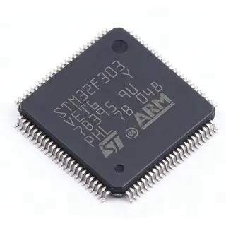
STM32F437VIT6 - 2MB Flash, 180MHz ARM Cortex-M4 MCU | STMicroelectronics
MPN: STM32F437VIT6 ✓ Active| Qty | Unit Price | Extended |
|---|---|---|
| 1 | $12.5 | $12.50 |
| 10 | $11.2 | $112.00 |
| 100 | $9.8 | $980.00 |
| 500 | $8.9 | $4,450.00 |
| 1,000 | $8.1 | $8,100.00 |
STM32F437VIT6 Overview
What is an ARM Cortex-M4 microcontroller? It is a 32-bit processor core designed for embedded systems, combining digital signal processing (DSP) instructions and a single-precision FPU for efficient handling of mathematical operations. The Cortex-M4 is part of the ARM Cortex-M family, which includes the M0, M0+, M3, M4, and M7 cores, each targeting different performance and power trade-offs. In the system hierarchy, a microcontroller integrates the processor core, memory, and peripherals on a single chip, enabling standalone operation in applications ranging from industrial control to consumer electronics.
Key features of the STM32F437VIT6 include a 180 MHz CPU with 225 DMIPS/1.25 DMIPS/MHz performance, a Chrom-ART Accelerator for enhanced graphical user interface (GUI) rendering, and a TFT LCD controller supporting up to XGA resolution. It also integrates a cryptographic/hash processor for AES, DES, and SHA-1/SHA-2 algorithms, a true random number generator (TRNG), and a camera interface. The device provides extensive connectivity with USB 2.0 OTG HS/FS, Ethernet MAC, CAN 2.0B, SPI, I2C, USART, and SDIO interfaces.
Technically, the STM32F437VIT6 is built on a 90 nm process technology, offering a balance of performance and power efficiency. It operates from a 1.8V to 3.6V power supply and includes multiple low-power modes (Sleep, Stop, Standby) to minimize energy consumption. The device supports external memory interfaces for SDRAM, SRAM, and NOR/NAND Flash, expanding its data storage capabilities beyond the internal 2 MB Flash.
Typical applications include industrial automation (PLC, motor control), medical devices (patient monitoring, diagnostic equipment), consumer electronics (smart home hubs, wearables), and IoT gateways. The combination of high performance, rich peripherals, and security features makes it a versatile choice for advanced embedded systems.
When designing with this MCU, ensure adequate decoupling on all power supply pins and follow the recommended layout for the 100-pin LQFP package. The internal LDO requires a 1.2V bypass capacitor, and the VBAT pin should be connected to a backup battery for RTC operation. Pay attention to the ADC reference voltage (VDDA) for accurate analog measurements.
Drop-in alternatives for STM32F437VIT6 — same package, pin-to-pin compatible. Different-package parts requiring PCB rework are excluded.
Variants in this series
Same-series models that are drop-in compatible with STM32F437VIT6 (same form factor and footprint) — differing in ADC, Communication Interfaces, Core, Flash Memory, Maximum Clock Frequency.
Quick Comparison Tool — Select alternative parts for side-by-side comparison:
STM32F437VGT6
✅ Drop-In ⚠️ 参数待验证📋 Reference alternative (not in catalog)
STM32F407VGT6
✅ Drop-In ⚠️ 参数待验证✓ In Stock
$7.55 / Unit
View Datasheet →STM32F429VIT6
✅ Drop-In ⚠️ 参数待验证📋 Reference alternative (not in catalog)
STM32F439VIT6
✅ Drop-In ⚠️ 参数待验证📋 Reference alternative (not in catalog)
LPC4370FET100
⚡ Same Package ⚠️ 参数待验证📋 Reference alternative (not in catalog)
STM32F437VIT6 Maximum Ratings & Electrical Characteristics
| Core | ARM Cortex-M4 with FPU |
| Maximum Clock Frequency | 180 MHz |
| Flash Memory | 2 MB |
| SRAM | 256 KB |
| Supply Voltage | 1.8 V to 3.6 V |
| Package | LQFP100 (14x14 mm, 0.5 mm pitch) |
| Operating Temperature | -40C to +85C |
| GPIO Pins | 82 |
| ADC | 3x 12-bit, 2.4 MSPS |
| DAC | 2x 12-bit |
| Timers | 12x 16-bit, 2x 32-bit |
| Communication Interfaces | USB 2.0 OTG HS/FS, Ethernet MAC, CAN 2.0B, SPI, I2C, USART, SDIO |
| Cryptographic Acceleration | AES, DES, SHA-1, SHA-2 |
| TFT LCD Controller | Up to XGA resolution |
| DMA | 2x DMA controllers with 16 streams each |
| RTC | Yes, with calendar and alarm |
| Low Power Modes | Sleep, Stop, Standby |
| RoHS Status | Compliant |
STM32F437VIT6 Pin Configuration
| Pin 1 | VBAT — Backup battery supply for RTC and backup registers |
| Pin 2 | PC13 — GPIO or RTC tamper/calendar output |
| Pin 3 | PC14 — GPIO or OSC32_IN |
| Pin 4 | PC15 — GPIO or OSC32_OUT |
| Pin 5 | PF0 — GPIO or OSC_IN |
| Pin 6 | PF1 — GPIO or OSC_OUT |
| Pin 7 | NRST — Reset (active low) |
| Pin 8 | PC0 — GPIO or ADC12_IN10 |
| Pin 9 | PC1 — GPIO or ADC12_IN11 |
| Pin 10 | PC2 — GPIO or ADC12_IN12 |
| Pin 11 | PC3 — GPIO or ADC12_IN13 |
| Pin 12 | VDD — Digital power supply (1.8V-3.6V) |
| Pin 13 | VSS — Digital ground |
| Pin 14 | PC4 — GPIO or ADC12_IN14 |
| Pin 15 | PC5 — GPIO or ADC12_IN15 |
| Pin 16 | PB0 — GPIO or ADC12_IN8 |
| Pin 17 | PB1 — GPIO or ADC12_IN9 |
| Pin 18 | PB2 — GPIO or BOOT1 |
| Pin 19 | PB10 — GPIO or I2C2_SCL/USART3_TX |
| Pin 20 | PB11 — GPIO or I2C2_SDA/USART3_RX |
| Pin 21 | VSS — Digital ground |
| Pin 22 | VDD — Digital power supply |
| Pin 23 | PB12 — GPIO or SPI2_NSS/I2S2_WS |
| Pin 24 | PB13 — GPIO or SPI2_SCK/I2S2_CK |
| Pin 25 | PB14 — GPIO or SPI2_MISO/I2S2_MCK |
| Pin 26 | PB15 — GPIO or SPI2_MOSI/I2S2_SD |
| Pin 27 | PD8 — GPIO or USART3_TX/FSMC_D13 |
| Pin 28 | PD9 — GPIO or USART3_RX/FSMC_D14 |
| Pin 29 | PD10 — GPIO or USART3_CK/FSMC_D15 |
| Pin 30 | PD11 — GPIO or USART3_CTS/FSMC_CLE |
| Pin 31 | PD12 — GPIO or USART3_RTS/FSMC_ALE |
| Pin 32 | PD13 — GPIO or FSMC_D0 |
| Pin 33 | PD14 — GPIO or FSMC_D1 |
| Pin 34 | PD15 — GPIO or FSMC_D2 |
| Pin 35 | PE0 — GPIO or FSMC_NBL0 |
| Pin 36 | PE1 — GPIO or FSMC_NBL1 |
| Pin 37 | PE2 — GPIO or FSMC_A23 |
| Pin 38 | PE3 — GPIO or FSMC_A19 |
| Pin 39 | PE4 — GPIO or FSMC_A20 |
| Pin 40 | PE5 — GPIO or FSMC_A21 |
| Pin 41 | PE6 — GPIO or FSMC_A22 |
| Pin 42 | VDD — Digital power supply |
| Pin 43 | VSS — Digital ground |
| Pin 44 | PE7 — GPIO or FSMC_D4 |
| Pin 45 | PE8 — GPIO or FSMC_D5 |
| Pin 46 | PE9 — GPIO or FSMC_D6 |
| Pin 47 | PE10 — GPIO or FSMC_D7 |
| Pin 48 | PE11 — GPIO or FSMC_D8 |
| Pin 49 | PE12 — GPIO or FSMC_D9 |
| Pin 50 | PE13 — GPIO or FSMC_D10 |
| Pin 51 | PE14 — GPIO or FSMC_D11 |
| Pin 52 | PE15 — GPIO or FSMC_D12 |
| Pin 53 | PB3 — GPIO or SPI1_SCK/TRACESWO |
| Pin 54 | PB4 — GPIO or SPI1_MISO/NJTRST |
| Pin 55 | PB5 — GPIO or SPI1_MOSI/I2C1_SMBA |
| Pin 56 | PB6 — GPIO or I2C1_SCL/USART1_TX |
| Pin 57 | PB7 — GPIO or I2C1_SDA/USART1_RX |
| Pin 58 | BOOT0 — Boot mode selection |
| Pin 59 | PB8 — GPIO or I2C1_SCL/CAN1_RX |
| Pin 60 | PB9 — GPIO or I2C1_SDA/CAN1_TX |
| Pin 61 | VSS — Digital ground |
| Pin 62 | VDD — Digital power supply |
| Pin 63 | PE0 — GPIO or TIM4_ETR/FSMC_NBL0 |
| Pin 64 | PE1 — GPIO or TIM4_CH1/FSMC_NBL1 |
| Pin 65 | PE2 — GPIO or TIM4_CH2/FSMC_A23 |
| Pin 66 | PE3 — GPIO or TIM4_CH3/FSMC_A19 |
| Pin 67 | PE4 — GPIO or TIM4_CH4/FSMC_A20 |
| Pin 68 | PE5 — GPIO or TIM9_CH1/FSMC_A21 |
| Pin 69 | PE6 — GPIO or TIM9_CH2/FSMC_A22 |
| Pin 70 | VDD — Digital power supply |
| Pin 71 | VSS — Digital ground |
| Pin 72 | PA0 — GPIO or TIM2_CH1/ADC12_IN0 |
| Pin 73 | PA1 — GPIO or TIM2_CH2/ADC12_IN1 |
| Pin 74 | PA2 — GPIO or TIM2_CH3/ADC12_IN2/USART2_TX |
| Pin 75 | PA3 — GPIO or TIM2_CH4/ADC12_IN3/USART2_RX |
| Pin 76 | PA4 — GPIO or SPI1_NSS/ADC12_IN4/DAC_OUT1 |
| Pin 77 | PA5 — GPIO or SPI1_SCK/ADC12_IN5/DAC_OUT2 |
| Pin 78 | PA6 — GPIO or SPI1_MISO/ADC12_IN6/TIM3_CH1 |
| Pin 79 | PA7 — GPIO or SPI1_MOSI/ADC12_IN7/TIM3_CH2 |
| Pin 80 | PA8 — GPIO or TIM1_CH1/USART1_CK/MCO1 |
| Pin 81 | PA9 — GPIO or TIM1_CH2/USART1_TX/USB_OTG_FS_VBUS |
| Pin 82 | PA10 — GPIO or TIM1_CH3/USART1_RX/USB_OTG_FS_ID |
| Pin 83 | PA11 — GPIO or TIM1_CH4/USART1_CTS/USB_OTG_FS_DM |
| Pin 84 | PA12 — GPIO or TIM1_ETR/USART1_RTS/USB_OTG_FS_DP |
| Pin 85 | PA13 — GPIO or JTMS-SWDIO |
| Pin 86 | VSS — Digital ground |
| Pin 87 | VDD — Digital power supply |
| Pin 88 | PA14 — GPIO or JTCK-SWCLK |
| Pin 89 | PA15 — GPIO or JTDI/TIM2_CH1_ETR |
| Pin 90 | PC10 — GPIO or UART4_TX/SDIO_D2 |
| Pin 91 | PC11 — GPIO or UART4_RX/SDIO_D3 |
| Pin 92 | PC12 — GPIO or UART5_TX/SDIO_CK |
| Pin 93 | PD0 — GPIO or FSMC_D2/OSC_IN |
| Pin 94 | PD1 — GPIO or FSMC_D3/OSC_OUT |
| Pin 95 | PD2 — GPIO or TIM3_ETR/SDIO_CMD |
| Pin 96 | PD3 — GPIO or USART2_CTS/FSMC_CLK |
| Pin 97 | PD4 — GPIO or USART2_RTS/FSMC_NOE |
| Pin 98 | PD5 — GPIO or USART2_TX/FSMC_NWE |
| Pin 99 | PD6 — GPIO or USART2_RX/FSMC_NWAIT |
| Pin 100 | PD7 — GPIO or USART2_CK/FSMC_NE1 |
Typical Applications
STM32F437VIT6 is suitable for 6 applications: Industrial Automation, Medical Devices, IoT Gateway, Consumer Electronics, Test and Measurement, Smart Home Hub.
Industrial Automation
The STM32F437VIT6 is ideal for industrial automation due to its 180 MHz Cortex-M4 core, advanced timers, and multiple communication interfaces. It can handle PLC logic, motor control, and HMI interfaces. The FPU accelerates PID algorithms, and the Ethernet MAC enables factory network connectivity. With 2 MB Flash, it can store complex control algorithms and diagnostics. The device's robust operating temperature range (-40C to +85C) ensures reliability in harsh environments. For motor control, the advanced timers generate PWM signals with dead-time insertion, and the ADCs sample current/voltage feedback at 2.4 MSPS. The CAN interface supports industrial fieldbuses, while the USB OTG allows local programming and data logging. The cryptographic acceleration secures communication with higher-level systems. Overall, the STM32F437VIT6 provides a single-chip solution for demanding industrial controllers.
Recommended
Medical Devices
In medical devices, the STM32F437VIT6 offers high performance and security features essential for patient monitoring and diagnostic equipment. The 180 MHz CPU processes biosignals in real-time, while the FPU handles filtering algorithms. The 2 MB Flash stores firmware and patient data, and the 256 KB SRAM buffers high-resolution ADC samples. The cryptographic acceleration ensures secure data transmission, complying with healthcare regulations. The TFT LCD controller drives graphical user interfaces for displays, and the camera interface can capture images for diagnostic tools. The device's low-power modes extend battery life in portable monitors. With multiple UARTs and SPI, it interfaces with sensors and wireless modules. The STM32F437VIT6's reliability and long-term availability make it suitable for medical-grade products.
Recommended
IoT Gateway
The STM32F437VIT6 is well-suited for IoT gateways, combining Ethernet MAC, USB OTG, and multiple wireless interfaces. The 180 MHz Cortex-M4 handles protocol stacks like MQTT and TLS, while the cryptographic acceleration offloads encryption tasks. The 2 MB Flash stores firmware and certificates, and the 256 KB SRAM buffers network packets. The device supports SDIO for external storage, and the camera interface can capture images for edge processing. With low-power modes, it can operate on battery backup during outages. The rich peripheral set allows connection to sensors via SPI, I2C, and UART. The STM32F437VIT6's security features (TRNG, crypto) ensure secure boot and communication, making it a robust choice for smart home and industrial IoT gateways.
Recommended
Consumer Electronics
In consumer electronics, the STM32F437VIT6 powers smart home hubs, wearables, and audio devices. The TFT LCD controller drives color displays, and the Chrom-ART accelerator enhances GUI rendering without CPU load. The 180 MHz CPU runs complex user interfaces and audio processing. The 2 MB Flash stores UI assets and audio samples, while the 256 KB SRAM handles dynamic data. The device supports USB OTG for charging and data transfer, and the camera interface enables image capture. Low-power modes extend battery life in portable devices. The cryptographic acceleration secures user data and communications. With a wide operating voltage range (1.8V-3.6V), it can run directly from Li-ion batteries. The STM32F437VIT6's rich feature set makes it a versatile choice for high-end consumer products.
Recommended
Test and Measurement
The STM32F437VIT6 is used in test and measurement equipment such as oscilloscopes, logic analyzers, and data loggers. The 180 MHz CPU and FPU handle signal processing, while the 2.4 MSPS ADCs capture high-speed analog signals. The 2 MB Flash stores firmware and calibration data, and the 256 KB SRAM buffers large data sets. The TFT LCD controller displays waveforms and measurements, and the USB OTG enables PC connectivity. The device's multiple timers generate precise trigger signals, and the DMA controllers transfer data without CPU intervention. The cryptographic acceleration secures firmware updates. With a wide operating temperature range, it is reliable in lab environments. The STM32F437VIT6's high performance and rich peripherals make it ideal for portable and benchtop instruments.
Recommended
Smart Home Hub
The STM32F437VIT6 serves as the central processor in smart home hubs, managing multiple wireless protocols (Zigbee, Z-Wave, Bluetooth) via external modules. The 180 MHz CPU runs the hub's operating system and protocol stacks, while the 2 MB Flash stores configuration and logs. The Ethernet MAC provides wired backbone connectivity, and the USB OTG allows local storage. The TFT LCD controller displays status and control interfaces. The cryptographic acceleration secures communication with cloud services. The device's low-power modes reduce energy consumption when idle. With multiple UARTs and SPI, it interfaces with various radio modules. The STM32F437VIT6's reliability and security features make it a trusted choice for smart home automation.
Recommended
Recommended Products Summary
Engineering reference data for STM32F437VIT6 — comparison, design guidance, and compliance information.
Selection Guide
Comparison with Alternatives
| Parameter | This Product | STM32F437VGT6 | STM32F407VGT6 | STM32F429VIT6 | STM32F439VIT6 | LPC4370FET100 |
|---|---|---|---|---|---|---|
| Package | LQFP100 | LQFP100 | LQFP100 | LQFP100 | LQFP100 | LQFP100 |
| Brand | STMicroelectronics | STMicroelectronics | STMicroelectronics | STMicroelectronics | STMicroelectronics | NXP Semiconductors |
| Core | ARM Cortex-M4 with FPU | ARM Cortex-M4 with FPU | ARM Cortex-M4 with FPU | ARM Cortex-M4 with FPU | ARM Cortex-M4 with FPU | ARM Cortex-M4 with FPU |
| Maximum Clock Frequency | 180 MHz | 180 MHz | 168 MHz | 180 MHz | 180 MHz | 204 MHz |
| Flash Memory | 2 MB | 2 MB | 1 MB | 2 MB | 2 MB | 1 MB |
| SRAM | 256 KB | 256 KB | 192 KB | 256 KB | 256 KB | 282 KB |
| TFT LCD Controller | Yes | Yes | No | Yes | Yes | Yes |
| Ethernet MAC | Yes | Yes | Yes | No | Yes | Yes |
| Cryptographic Acceleration | Yes | Yes | No | Yes | Yes | No |
Key Differentiators
- 2 MB Flash and 256 KB SRAM in LQFP100 (vs STM32F407VGT6)
- Integrated TFT LCD controller and Chrom-ART accelerator (vs STM32F407VGT6)
- Cryptographic acceleration and TRNG (vs LPC4370FET100)
Design Notes
The STM32F437VIT6 requires a 1.8V to 3.6V power supply. Decouple each VDD pin with a 100nF ceramic capacitor and a 4.7uF bulk capacitor. The VDDA pin (analog supply) should be filtered with a ferrite bead and a 1uF capacitor to reduce noise for ADC accuracy. The VBAT pin must be connected to a backup battery (1.65V to 3.6V) for RTC operation when main power is off. Ensure the internal LDO's 1.2V bypass capacitor (VCAP1 and VCAP2 pins) is placed close to the pins with a 2.2uF low-ESR capacitor.
For the LQFP100 package, follow the recommended land pattern in the datasheet. Use a 4-layer PCB with dedicated power and ground planes. Place decoupling capacitors as close as possible to the power pins. For the crystal oscillator (OSC_IN/OSC_OUT), keep traces short and shielded with ground pour to minimize noise. The NRST pin should have a 100nF capacitor to ground for reset filtering. For high-speed interfaces like USB and Ethernet, maintain controlled impedance (90 ohms differential for USB, 100 ohms for Ethernet) and keep trace lengths matched.
A common mistake is forgetting to connect the VCAP pins (VCAP1 and VCAP2) with the required 2.2uF capacitor, which can cause the device to fail to start. Also, ensure the BOOT0 pin is properly configured; leaving it floating can cause unexpected boot behavior. For ADC accuracy, avoid routing digital signals near the VDDA pin. When using the TFT LCD controller, ensure the pixel clock and synchronization signals are correctly configured to avoid display artifacts. Finally, do not exceed the absolute maximum ratings on any pin, especially during programming.
Compliance Information
STMicroelectronics products are RoHS compliant and lead-free. The STM32F437VIT6 is not AEC-Q100 qualified; for automotive, consider the STM32F437VIT6TR or other automotive-grade variants.